Article

The Variation of Schottky Barrier Height Induced by the Phase Separation of InAlAs Layers on InP HEMT Devices

1
Korea-Advanced-Nano-Center (KANC), Suwon 16229, Korea
2
Samsung Display Co., Ltd., Yongin-Si 17113, Korea
3
Department of Electrical and Computer Engineering, Inter-University Semiconductor Research Center, Seoul National University (SNU), Seoul 08826, Korea
4
Department of Material Science and Engineering, Yonsei University, Seoul 03722, Korea
5
School of Electronics Engineering, Kyungpook National University (KNU), Daegu 41566, Korea
*
Authors to whom correspondence should be addressed.
These authors contributed equally to this work.
Crystals 2022, 12(7), 966; https://doi.org/10.3390/cryst12070966
Submission received: 13 June 2022 / Revised: 29 June 2022 / Accepted: 5 July 2022 / Published: 11 July 2022

Abstract

:
We investigated the effect of phase separation on the Schottky barrier height (SBH) of InAlAs layers grown by metal–organic chemical vapor deposition. The phase separation into the In-rich InAlAs column and Al-rich InAlAs column of In0.52Al0.48As layers was observed when we grew them at a relatively low temperature of below 600 °C. From the photoluminescence spectrum investigation, we found that the band-gap energy decreased from 1.48 eV for a homogeneous In0.52Al0.48As sample to 1.19 eV for a phase-separated InxAl1−xAs sample due to the band-gap lowering effect by In-rich InxAl1−xAs (x > 0.7) region. From the current density–voltage analysis of the InAlAs Schottky diode, it was confirmed that the phase-separated InAlAs layers showed a lower SBH value of about 240 meV than for the normal InAlAs layers. The reduction in SBH arising from the phase separation of InAlAs layers resulted in the larger leakage current in InAlAs Schottky diodes.

1. Introduction

InP-based high electron mobility transistor (InP-HEMT) with characteristics of ultra-low noise and high on/off speed shows remarkable DC and RF properties [1,2,3]. It is well known that the InP-HEMT consists of an InP lattice-matched In0.53Ga0.47As channel and an In0.52Al0.48As buffer and barrier [4,5]. InP-HEMT for the ultra-high frequency RF applications of 850 GHz should have such characteristics as a high resistivity of the InAlAs buffer, a high electron mobility of the InGaAs channel, high gate capacitance, and low leakage current of the InAlAs barrier [6]. Among them, there are many studies on metal/semiconductor contacts to reduce gate leakage current by forming a Schottky contact with a large barrier height over 830 meV between the InAlAs barrier layers and Pt [7], Cr [8], and Ir [9] layers.
Generally, the gate leakage current in InP HEMTs with InAlAs Schottky barrier layers grown using metal–organic chemical vapor deposition (MOCVD) or molecular beam epitaxy (MBE) methods is related to the thermionic emission of charges or defect-assisted tunneling, which arises from a low Schottky barrier height formed by poor crystallinities of the InAlAs barrier [10]. In particular, the InAlAs epitaxial layers show a specific phenomenon such as phase separation depending on the growth parameters, especially growth temperatures [11,12,13]. Phase separation is caused by the surface mobility difference of In and Al ad-atoms, deriving the local composition fluctuations during the growth. Phase-separated InAlAs layers grown at insufficient temperature led to surface roughness and band-gap lowering by local In-rich InAlAs regions. Nevertheless, a few studies have been conducted on the effect of phase separation of the InAlAs Schottky barrier layer’s electrical properties on InP HEMT devices.
In this article, we report the investigation results on the effect of phase separation of InAlAs Schottky barrier layers grown by MOCVD. In the phase-separated InAlAs, the lowering of the band-gap energy was observed from photoluminescence (PL) spectrum. The Schottky barrier height (SBH) was measured from InAlAs Schottky diodes fabricated on n+InP (100) substrates. From the SBH results calculated by thermionic emission theory, it was found that the phase-separated InAlAs samples showed a low barrier height of ~300 meV at 300 K compared to normal InAlAs layers.

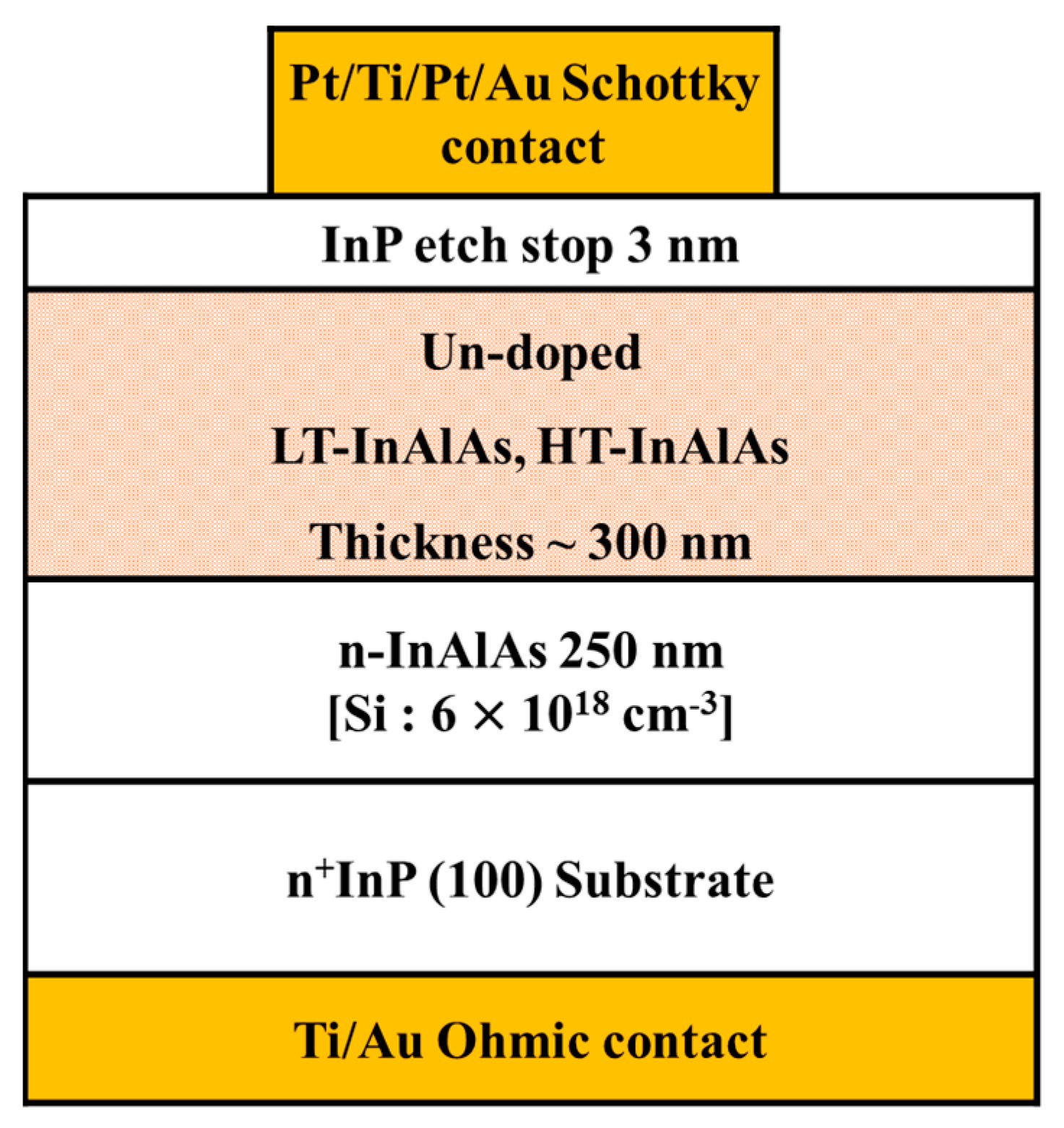
2. Materials and Methods

The InAlAs layer was grown at 500 °C (low-temperature, LT) and 660 °C (high-temperature, HT) using an MOCVD system (AIX200 4/L, Aixtron, Herzogenrath, Germany). Trimethylaluminum (TMAl), trimethylindium (TMIn), hydride-gas arsine (AsH3), and phosphine (PH3) were used as precursors and hydrogen gas was used as carrier gas with a total flow of 15 slm for epitaxial growth. All samples were grown at a V/III ratio of 100, and a total pressure of 160 mbar in reactor. TMIn and TMAl flow amounts for LT-InAlAs growth at 500 °C were 17.01 μmol/min and 4.36 μmol/min, respectively. The Indium content x, determined by a high-resolution X-ray diffraction (HR-XRD) measurement in InxAl1−xAs layer was x = 0.520. For the HT-InAlAs growth at 660 °C, 17.86 μmol/min of TMIn and 4.36 μmol/min of TMAl were used and obtained the InxAl1−xAs layer with a x = 0.512.
For the analysis of structural and surface morphology, the InAlAs layers with the same growth conditions as in Schottky diode samples were grown on Fe-doped semi-insulting InP (100) substrates. The surface morphology and roughness were measured using atomic force microscopy (AFM). The crystal structure and local composition variation in InAlAs layers according to the growth temperature were investigated using high-angle annular dark-field (HAADF) scanning transmission electron microscopy (STEM) observation. The effect of phase separation on the bandgap energy of InAlAs was analyzed by room temperature PL. The 266 nm line of Q-switch laser with the power density of 210 mW/cm2 was used for excitation. The InAlAs Schottky diodes consist of 250-nm-thick Si doped (6 × 1018 cm−3) In0.52Al0.48As buffer layer grown at 660 °C on n+InP (100) substrate and 300-nm-thick LT- or HT-InAlAs Schottky contact layers, as shown in Figure 1. After hydride switching from AsH3 to 25 sccm of PH3, the 3-nm-thick InP etch stop layer was grown at 500 °C to suppress the formation of native oxide on the surface of the InAlAs layer. The stack of Schottky contact was Au/Pt/Ti/Pt (300/10/10/80 nm), and the contact metal area was 4.0 × 10⁻⁴ cm2. The ohmic contact was formed using Au/Ti (300/10 nm) on the back side of n+InP (100) substrate. The background donor density of the un-doped InAlAs layer was estimated by capacitance–voltage (C–V) measurement at 300 K. The leakage current of InAlAs Schottky diodes were analyzed by current density–voltage (J–V) measurements at 77 K and 300 K. Additionally, the Schottky barrier height (SBH) was estimated using thermionic current–voltage relationship.

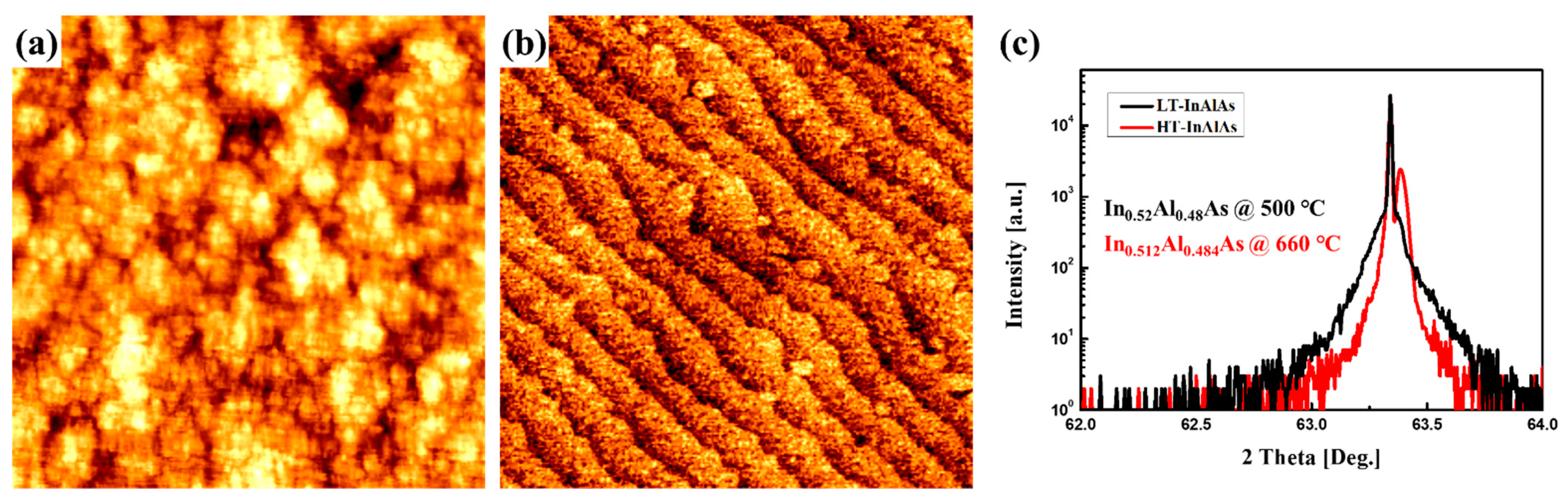
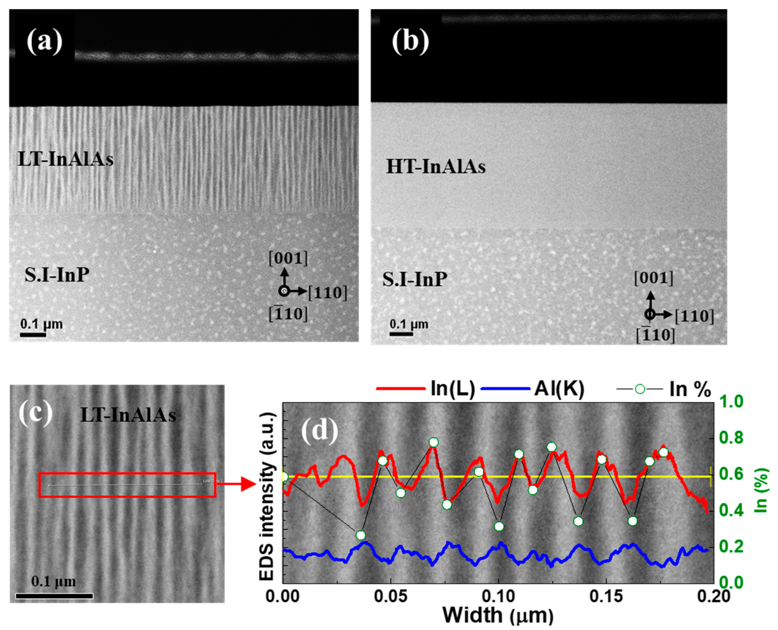
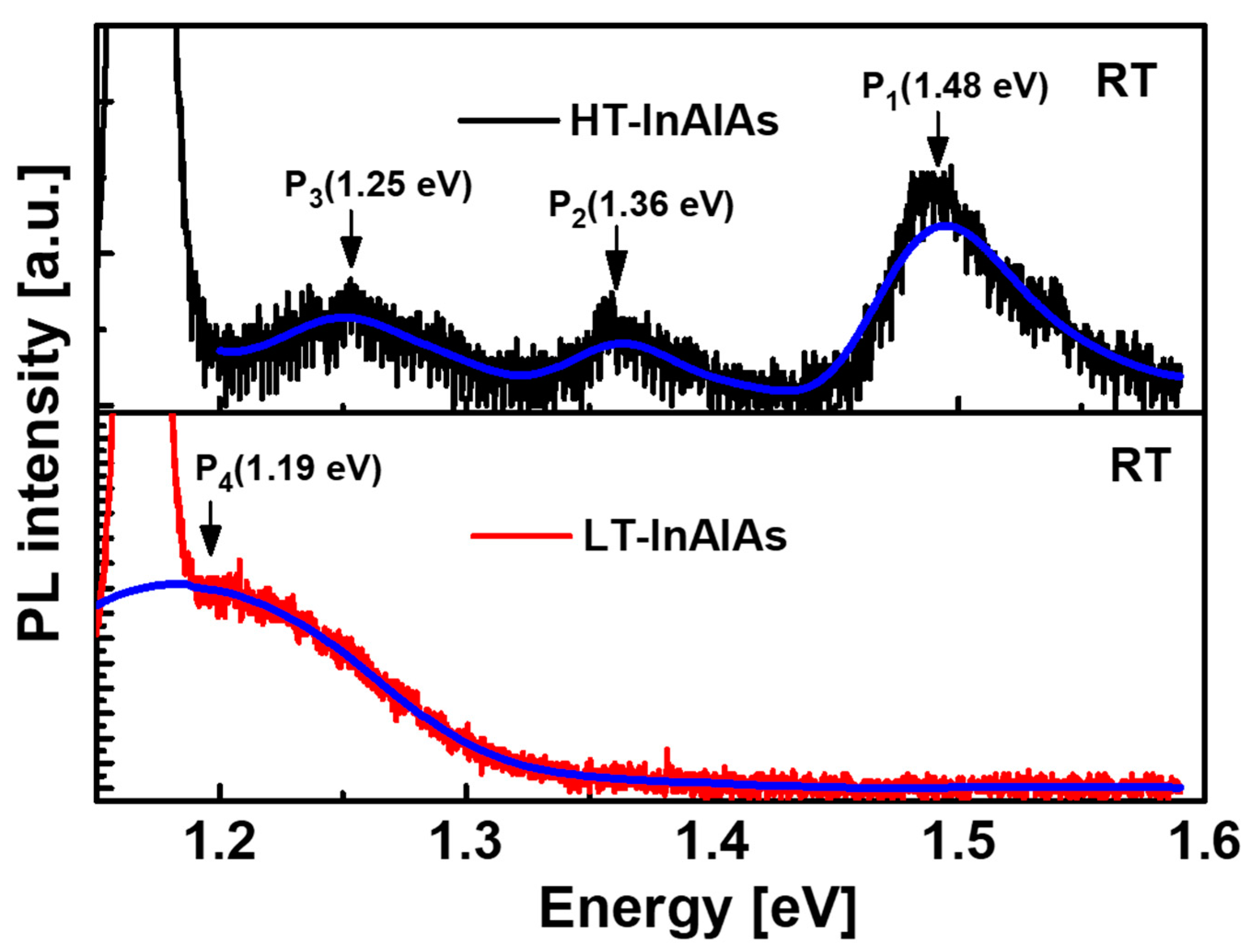
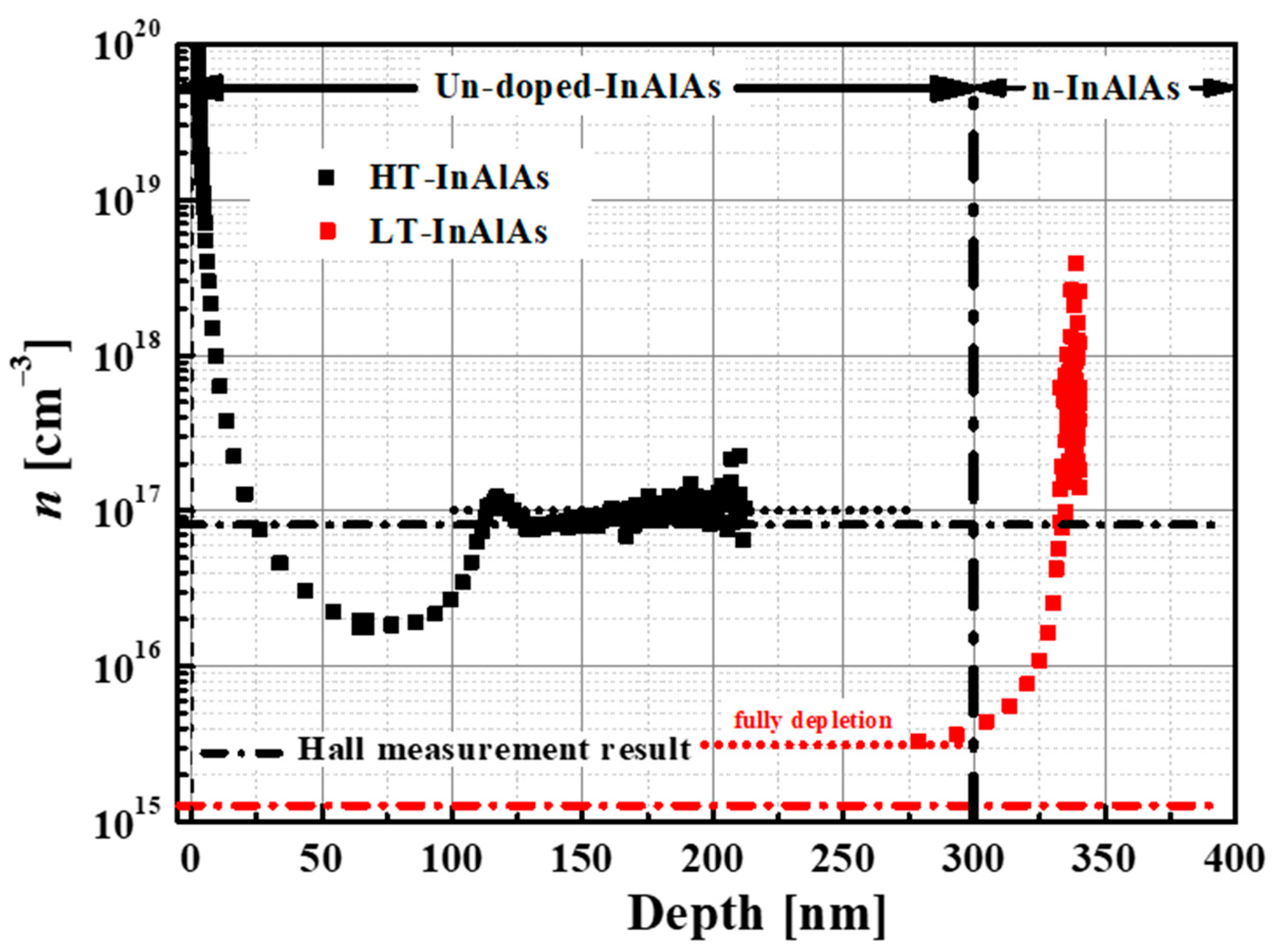
3. Results and Discussion

Figure 2 shows 3 × 3 μm2 AFM images for the (a) LT-InAlAs and (b) HT-InAlAs samples grown on semi-insulating InP (100) substrates. While the LT-InAlAs sample has a mound structured surface with a root mean square (RMS) roughness of 0.7 nm, the HT-InAlAs sample shows a clear terrace-like surface, indicating step flow growth with an RMS roughness of 0.1 nm as shown in Figure 2b. The In composition measured in HR-XRD scans are shown in Figure 2c.
Cross-sectional STEM images obtained at [110] zone axis for the corresponding samples with Figure 2 are shown in Figure 3. The LT-InAlAs sample as shown in Figure 3a shows columnar structure with different brightness, which originated from the composition fluctuation by phase separation of InAlAs layers as discussed in Ref. [14], with about 10 nm diameter. In contrast, cross-sectional STEM image in Figure 3b for the HT-InAlAs sample shows a flat and homogeneous in composition. In/Al composition variation of the LT-InAlAs sample showing the phase-separated columnar structure, investigated using energy dispersive X-ray spectroscopy (EDS) profile, is shown in Figure 3d for the line indicated in Figure 3c. The In composition in the columns periodically fluctuated from about 70% at peak to about 30% at valley with an average value of about 55.7%. This means that there are two phases with different columnar compositions in LT-InAlAs samples, and this phase separation occurred during growth at relatively low temperature. The In composition measured in HR-XRD scans for the LT-InAlAs layer in Figure 2c was 52% and we could not distinguish phase separation from ω-2θ scans as distinguished in STEM analysis. The formation of the mounded surface and phase separation of the LT-InAlAs layers mainly originated from the low mobility of ad-atoms on the growing surface at a low growth temperature as discussed in [15].
Figure 4 shows the PL spectra measured at room temperature for the LT-InAlAs and HT-InAlAs samples grown on semi-insulating InP (100) substrates. In the HT-InAlAs sample, three peaks located at P1 = 1.48 eV, P2 = 1.36 eV, and P3 = 1.25 eV are observed. We estimated that those PL peaks are originated from PL transitions in the In0.51Al0.49As (P1), InP (P2), and In0.52Al0.48As/InP interface (P3), respectively [16,17]. Generally, the PL transitions for InxAl1−xAs layers are related to the bandgap energy which varies with the In composition x. When In composition x = 0.51–0.52, the band-gap energy measured by PL is 1.46–1.48 eV at room temperature. In contrast, the PL spectrum of LT-InAlAs showing phase separation was broad with only one peak at 1.19 eV (P4). The band gap energy of 1.19 eV for InxAl1−xAs corresponds to x = 0.65 when it is estimated from the Vegard’s law [18]. According to STEM EDS results shown in Figure 3d for LT-InAlAs sample, the In composition x was varied with column in the range of 0.26 and 0.78. Additionally, it is well known that InxAl1−xAs shows indirect transition characteristics when the In composition x is less than 0.3. Therefore, we can deduce that the PL signal in the Al-rich column with x ~ 0.26 in LT-InAlAs sample might not be detected. Because the band gap energy for InxAl1−xAs layer with x = 0.70 is expected to 0.91 eV, the 1.19 eV of P4 peak for LT-InAlAs layer shifted to the higher band gap energy than x = 0.70. We attribute this red shift of bandgap energy of phase-separated LT-InAlAs layers to a confinement effect of In-rich columns which are surrounded by quantum barriers with the Al-rich columns as discussed in a Ge/InAlAs nano-composite structure with phase separation as described in Ref. [19]. The similar phenomena of bandgap lowering in InAlAs epitaxial layers has been reported in several studies, in which those were occurred by phase separation or Cu-Pt type ordering in InAlAs epitaxial layers [13]. The similar lowering of the Schottky barrier height with the In composition of InAlAs is reported in [20].
Figure 5 shows the depth profile obtained from the room temperature (RT) C–V measurements on the HT- and LT-InAlAs Schottky diode samples described in Figure 1. The capacitance was measured from V = −2 V to 0.5 V. The x-axis and y-axis of Figure 5 were calculated by the relationship between the carrier concentration and depth [21], given by:
C = ϵ A x d
n ( x d ) = 2 q ϵ A 2 [ d C 2 d V ] 1
where C is capacitance, ϵ is permittivity, A is area, x d is depletion depth, and n is carrier concentration. As indicated by dot lines in Figure 5, the concentrations of donors were ~3.0 × 1015 cm−3 for the LT-InAlAs layer and 0.8 to 1.0 × 1017 cm−3 for the HT-InAlAs layer, respectively. These n values obtained from the RT Hall effects measurement using the Van der Pauw pattern were similar with ~1.0 × 1015 cm−3 for LT-InAlAs and ~8.0 × 1016 cm−3 for HT-InAlAs, respectively. The difference in resistivity values for two samples were huge, with about five-order higher at the LT-InAlAs with ~1.0 × 10⁴ Ω·cm than for HT-InAlAs with 0.1 Ω·cm.
Figure 6 shows semi-logarithmic J versus V curve results at 77 K and 300 K of LT- and HT-InAlAs Schottky diodes. Regardless of the measurement temperature, high current densities are observed in both the reverse and forward directions of the LT-InAlAs Schottky diode. Specifically, the leakage current densities of HT-InAlAs Schottky diodes at −2 V are 4.4 × 10⁻⁴ A/cm2 at 300 K and 3.1 × 10⁻⁴ A/cm2 at 77 K, whereas 2.9 × 10⁻² A/cm2 at 300 K and 9.0 × 10⁻³ A/cm2 at 77 K for LT-InAlAs, respectively. According to the C–V and Hall effect results, the LT-InAlAs layer has higher resistive properties due to the lower background carrier concentration than HT-InAlAs. The lower current of the LT-InAlAs at the forward bias region of the J–V plot comes from this resistance difference. However, the J–V plot at the reverse bias region shows an opposite trend, i.e., the LT-InAlAs Schottky diodes at both 300 K and 77 K show more conductive properties than HT-InAlAs Schottky diodes. There are more conductive properties in the LT-InAlAs layers in Schottky diodes at the reverse bias, as shown in Figure 6, even though they have higher resistivity values and a lower carrier concentration as discussed in Figure 5. This could be understood by the formation of a low SBH at the metal/LT-InAlAs junction. Additionally, from the temperature dependent J–V curves, it is identified that the leakage current of LT-InAlAs Schottky diode is not sufficiently suppressed at 77 K, compared to HT-InAlAs Schottky diode. The high leakage current even at low temperature measurement clearly indicates the dominance of the band-gap lowering effect by phase separation rather than trap-assisted-tunneling (TAT).
We estimated SBH at 77 K and 300 K using thermionic emission theory from the J–V curve of an InAlAs Schottky diode. The thermionic current density–voltage relationship of a Schottky diode, neglecting series and shunt resistance [22,23], is given by:
J = J s ( e x p ( q V n k T ) 1 )
where Js is the saturation current density given by:
J s = A * T 2 e x p ( q ϕ B k T )
In (3) and (4), q is element charge constant, V is bias voltage, n is the ideality factor, T is the absolute temperature, k is the Boltzmann constant, ϕB is the SBH, and A* is the effective Richardson’s constant (9.2 A⋅cm−2⋅K−2) for InAlAs [24]. The SBH is calculated from Js obtained from the measured value and is defined as:
ϕ B = kT q l n ( A * T 2 J s )
From the result of a linear plot of the forward bias region in the semi-logarithmic J versus V curve in Figure 6, Js is the intercept of the current density axis at zero bias. The Js of InAlAs Schottky diodes 77 K and 300 K were 8.34 × 10⁻³ A/cm2 and 9.40 × 10⁻³ A/cm2 for LT-InAlAs, 2.27 × 10⁻⁶ A/cm2 and 1.11 × 10⁻⁶ A/cm2 for HT-InAlAs, respectively. The SBH calculated by (5) for LT-InAlAs, as shown in the Table 1, is 0.10 eV at 77 K and 0.47 eV at 300 K. On the other hand, HT-InAlAs resulted in high SBH with 0.16 eV at 77 K and 0.71 eV at 300 K, respectively. These temperature-dependent phenomena of SBH and n are explained by the current transport by the thermally activated process at the metal/semiconductor interface [25,26]. In the J–V curve in Figure 6, the leakage current is caused by thermal emission of electrons that overcome the SBH at 77 K and 300 K. As a result, the effective barrier height is expected to be temperature dependent. The difference of 240 meV of SBH between LT- and HT-InAlAs Schottky diode at 300 K measured by J–V curve meets well with the 290 meV of band-gap lowering measured by PL measurement. In addition, the ideality factor n values for the LT-InAlAs were 13.1 at 77 K and 3.35 at 300 K and for the HT-InAlAs were 5.72 at 77 K and 1.17 at 300 K, respectively. The high ideality factor at the LT-InAlAs is attributed to the combined effect of the interface state, image force lowering, and tunneling at the metal/semiconductor interface [24]. The high leakage current induced by tunneling at metal/semiconductor interface increased the ideality factor at the low forward bias region. In addition, high resistivity of the LT-InAlAs layer, as discussed in Figure 5, also lowered the ideality factor by reducing on-current.
In summary, Schottky diodes with LT-InAlAs show high leakage current due to the SBH lowering, which originated from the In-rich InAlAs column, as identified in the EDS and PL analyses. Even though LT-InAlAs has very high resistivity value as discussed in the C–V and Hall effect measurement, which is a necessary condition for the buffer layer, but is not proper for the Schottky barrier layer because the phase-separated In-rich region gives SBH lowering, and this results in a larger gate leakage current in HEMT.

4. Conclusions

We investigated the effect of the phase separation of the InAlAs layer on SBHs through the evaluation of Schottky diodes. The phase separation with the In-rich column and Al-rich column occurred at the LT-InAlAs layers grown on InP (100) substrates at 500 °C by MOCVD. The phase separation of LT-InxAl1−xAs resulted in the decrease in the band-gap that originated from the In-rich column with x > 70%. Even though the LT-InAlAs layer also showed a high resistivity value (>1.0 × 10⁴ Ω·cm) arising from the low background carrier of 1.0 × 1015 cm−3, it showed a high leakage current on Schottky diode application. The SBH values estimated by thermionic emission theory for LT-InAlAs formed at lower values with 60 meV at 77 K and 240 meV at 300 K than HT-InAlAs, respectively. This lowering of SBH of the LT-InAlAs layer leads to the high leakage current of Schottky diode.

Author Contributions

Conceptualization, S.-T.L., M.K., C.-S.S. and K.-S.S.; methodology, S.-T.L. and C.-S.S.; formal analysis, S.-T.L. and M.K.; investigation, S.-T.L., M.K., H.J., C.-H.S., D.-Y.Y. and H.-s.J.; resources, H.J., S.K., D.-H.K. and C.-S.S.; writing—original draft preparation, S.-T.L. and M.K.; writing—review and editing, S.-T.L. and M.K.; supervision, D.-H.K., C.-S.S. and K.-S.S.; funding acquisition, D.-H.K., C.-S.S. and K.-S.S. All authors have read and agreed to the published version of the manuscript.

Funding

This research was supported by both the Civil-Military Technology Cooperation program (NO. 19-CM-BD-05) and the Grant No. NRF-2022M3I8A1085446 of the National Research Foundation of Korea (NRF), Ministry of Science and ICT, in Korea.

Institutional Review Board Statement

Not applicable.

Informed Consent Statement

Not applicable.

Data Availability Statement

The data presented in this study are available on request from the corresponding author.

Conflicts of Interest

The authors declare no conflict of interest.

References

  1. Shiratori, Y.; Hoshi, T.; Ida, M.; Higurashi, E.; Matsuzaki, H. High-speed InP/InGaAsSb DHBT on high-thermal-conductivity SiC substrate. IEEE Electron. Device Lett. 2018, 39, 807–810. [Google Scholar] [CrossRef]
  2. Jo, H.B.; Yun, D.Y.; Baek, J.M.; Lee, J.H.; Kim, T.W.; Kim, D.H.; Tsutsumi, T.; Sugiyama, H.; Matsuzaki, H. Lg = 25 nm InGaAs/InAlAs high-electron mobility transistors with both fT and fmax in excess of 700 GHz. Appl. Phys. Express 2019, 12, 054006. [Google Scholar] [CrossRef]
  3. Sugiyama, H.; Matsuzaki, H.; Yokoyama, H.; Enoki, T. High-electron-mobility In0.53Ga0.47As/In0.8Ga0.2As composite-channel modulation-doped structures grown by metal-organic vapor-phase epitaxy. In Proceedings of the 2010 22nd International Conference on Indium Phosphide and Related Materials (IPRM 2010), Takamatsu, Japan, 31 May–4 June 2010; pp. 1–4. [Google Scholar] [CrossRef]
  4. Sugiyama, Y.; Takeuchi, Y.; Tacano, M. High electron mobility pseudomorphic In0.52Al0.48As/In0.8Ga0.2As heterostructure on InP grown by flux-stabilized MBE. J. Cryst. Growth 1991, 115, 509–514. [Google Scholar] [CrossRef]
  5. Brown, A.S.; Nguyen, L.D.; Metzger, R.A.; Schmitz, A.E.; Henige, J.A. Growth and properties of high mobility strained inverted AlInAs–GaInAs modulation doped structures. J. Vac. Sci. Technol. B 1992, 10, 1017–1019. [Google Scholar] [CrossRef]
  6. Suemitsu, T. InP and GaN high electron mobility transistors for millimeter-wave applications. IEICE Electron. Express 2015, 12, 20152005. [Google Scholar] [CrossRef] [Green Version]
  7. Kim, S.; Adesida, I.; Hwang, H. Measurements of thermally induced nanometer-scale diffusion depth of Pt/Ti/Pt/Au gate metallization on InAlAs/InGaAs high-electron-mobility transistors. Appl. Phys. Lett. 2005, 87, 232102. [Google Scholar] [CrossRef]
  8. Harada, N.; Kuroda, S.; Katakami, T.; Hikosaka, K.; Mimura, T.; Abe, M. Pt-based gate enhancement-mode InAlAs/InGaAs HEMTs for large-scale integration. In Proceedings of the Third International Conference Indium Phosphide and Related Materials, Cardiff, UK, 8–11 April 1991; pp. 377–380. [Google Scholar] [CrossRef]
  9. Wang, L.; Zhao, W.; Adesida, I. Correlating the Schottky barrier height with the interfacial reactions of Ir gates for InAlAs/InGaAs high electron mobility transistors. Appl. Phys. Lett. 2006, 89, 211910. [Google Scholar] [CrossRef]
  10. Luo, J.K.; Thomas, H.; Clark, S.A.; Williams, R.H. The effect of growth temperature on the electrical properties of AlInAs/InP grown by molecular beam epitaxy and metal-organic chemical-vapor deposition. J. Appl. Phys. 1993, 74, 6726. [Google Scholar] [CrossRef]
  11. Jun, S.W.; Seong, T.Y.; Lee, J.H.; Lee, B. Naturally formed InxAl1−xAs/InyAl1−yAs vertical superlattices. Appl. Phys. Lett. 1996, 68, 3443–3445. [Google Scholar] [CrossRef]
  12. Yoon, S.F.; Miao, Y.B.; Radhakrishnan, K.; Swaminathan, S. Photoluminescence and raman scattering characterization of silicon-doped In0.52Al0.48As grown on InP (100) substrates by molecular beam epitaxy. J. Electron. Mater. 1996, 25, 1458–1462. [Google Scholar] [CrossRef]
  13. Kondow, M.; Kakibayashi, H.; Minagawa, S.; Inoue, Y.; Nishino, T.; Hamakawa, Y. Crystalline and electronic energy structure of OMVPE-grown AlGaInP/GaAs. J. Cryst. Growth 1988, 93, 412–417. [Google Scholar] [CrossRef]
  14. Kurihara, K.; Takashima, M.; Sakata, K.; Ueda, R.; Takahara, M.; Ikeda, H.; Namita, H.; Nakamura, T.; Shimoyama, K. Phase separation in InAlAs grown by MOVPE with a low growth temperature. J. Cryst. Growth 2004, 271, 341–347. [Google Scholar] [CrossRef]
  15. Lu, Y.; Wang, C.P.; Liu, X.J. Calculation of phase diagrams in AlxIn1−xAs/InP, AsxSb1−xAl/InP and AlxIn1−xSb/InSb nano-film systems. J. Cryst. Growth 2009, 311, 4374–4380. [Google Scholar] [CrossRef]
  16. Böhrer, J.; Krost, A.; Bimberg, D. Spatially indirect intersubband transitions of localized electrons and holes at the staggered band lineup In0.52Al0.48As/InP interface. J. Vac. Sci. Technol. B 1993, 11, 1642–1646. [Google Scholar] [CrossRef]
  17. Gilinsky, A.M.; Dmitriev, D.V.; Toropov, A.I.; Zhuravlev, K.S. Defect-related luminescence in InAlAs on InP grown by molecular beam epitaxy. Semicond. Sci. Technol. 2017, 32, 095009. [Google Scholar] [CrossRef]
  18. Ivanov, S.V.; Chernov, M.Y.; Solov’ev, V.A.; Brunkov, P.N.; Firsov, D.D.; Komkov, O.S. Metamorphic InAs(Sb)/InGaAs/InAlAs nanoheterostructures grown on GaAs for efficient mid-IR emitters. Prog. Cryst. Growth Charact. Mater. PROG 2019, 65, 20–35. [Google Scholar] [CrossRef]
  19. Jung, D.; Faucher, J.; Mukherjee, S.; Akey, A.; Ironside, D.J.; Cabral, M.; Sang, X.; Lebeau, J.; Bank, S.R.; Buonassisi, T.; et al. Highly tensile-strained Ge/InAlAs nanocomposites. Nat. Commun. 2017, 8, 14204. [Google Scholar] [CrossRef] [PubMed] [Green Version]
  20. Lin, C.L.; Chu, P.; Kellner, A.L.; Wieder, H.H.; Rezek, E.A. Composition dependence of Au/InxAl1−xAs Schottky barrier heights. Appl. Phys. Lett. 1986, 49, 1593–1595. [Google Scholar] [CrossRef]
  21. Sze, S.M. Semiconductor Devices: Pioneering Papers, 2nd ed.; World Scientific: Singapore, 1991. [Google Scholar]
  22. Rao, P.K.; Park, B.; Lee, S.T.; Noh, Y.K.; Kim, M.D.; Oh, J.E. Analysis of leakage current mechanisms in Pt/Au Schottky contact on Ga-polarity GaN by Frenkel-Poole emission and deep level studies. J. Appl. Phys. 2011, 110, 013716. [Google Scholar] [CrossRef]
  23. Schroder, D.K. Semiconductor Material and Device Characterization, 3rd ed.; John Wiley & Sons: Hoboken, NJ, USA, 2015. [Google Scholar]
  24. Hamdaoui, N.; Ajjel, R.; Salem, B.; Gendry, M. Distribution of barrier heights in metal/n-InAlAs Schottky diodes from current–voltage–temperature measurements. Mater. Sci. Semicond. Process. 2014, 26, 431–437. [Google Scholar] [CrossRef]
  25. Werner, J.H.; Güttler, H.H. Barrier inhomogeneities at Schottky contacts. J. Appl. Phys. 1991, 69, 1522–1533. [Google Scholar] [CrossRef]
  26. Tung, R.T. Electron transport at metal-semiconductor interfaces: General theory. Phys. Rev. B 1992, 45, 13509. [Google Scholar] [CrossRef] [PubMed]
Figure 1. A schematic diagram of a Schottky diode with LT- and HT-InAlAs barriers.
Crystals 12 00966 g001
Figure 2. AFM (3 × 3 μm2) scans showing surface morphologies of InAlAs layers grown at a temperature of (a) 500 °C and (b) 660 °C. (c) Corresponding HR-XRD ω-2θ scan data.
Crystals 12 00966 g002
Figure 3. Cross-sectional STEM images for InAlAs grown at a temperature of (a) 500 °C and (b) 660 °C. (d) is an EDS line scan obtained from the dashed rectangle in (c), a magnified image of the InAlAs layer in (a). The red and blue lines indicate In(L) and Al(K) intensities measured from EDS, and green circles indicate corresponding In composition at specific points.
Crystals 12 00966 g003
Figure 4. Room temperature PL spectrum for HT-InAlAs (top) and LT-InAlAs (bottom). The fitted spectra are drawn with blue lines.
Crystals 12 00966 g004
Figure 5. Depth profiles of donor density n extracted from C–V measurement of HT- and LT-InAlAs Schottky diodes with a metal contact area of 4.0 × 10⁻⁴ cm−2. The donor concentration values from the Hall measurement are indicated as dashed dot lines.
Crystals 12 00966 g005
Figure 6. Semi-logarithmic current density–voltage graphs of HT- and LT-InAlAs Schottky diodes measured at 77 K and 300 K. Schottky contact area is 4 × 10⁻⁴ cm−2.
Crystals 12 00966 g006
Table 1. Calculated values of SBH and ideality factor n from Figure 6 (fitted between 0.1 to 0.4 V).
SampleDiode Area (cm−2)SBH (eV)Ideality Factor (n)
@ 77 K@ 300 K@ 77 K@ 300 K
LT-InAlAs4.0 × 10−40.100.4713.13.35
HT-InAlAs0.160.715.721.17
Publisher’s Note: MDPI stays neutral with regard to jurisdictional claims in published maps and institutional affiliations.

