

The Variation of Schottky Barrier Height Induced by the Phase Separation of InAlAs Layers on InP HEMT Devices
 ,
,
Abstract
1. Introduction
2. Materials and Methods
3. Results and Discussion
4. Conclusions
Author Contributions
Funding
Institutional Review Board Statement
Informed Consent Statement
Data Availability Statement
Conflicts of Interest
References
- Shiratori, Y.; Hoshi, T.; Ida, M.; Higurashi, E.; Matsuzaki, H. High-speed InP/InGaAsSb DHBT on high-thermal-conductivity SiC substrate. IEEE Electron. Device Lett. 2018, 39, 807–810. [Google Scholar] [CrossRef] [Scilit]
- Jo, H.B.; Yun, D.Y.; Baek, J.M.; Lee, J.H.; Kim, T.W.; Kim, D.H.; Tsutsumi, T.; Sugiyama, H.; Matsuzaki, H. Lg = 25 nm InGaAs/InAlAs high-electron mobility transistors with both fT and fmax in excess of 700 GHz. Appl. Phys. Express 2019, 12, 054006. [Google Scholar] [CrossRef] [Scilit]
- Sugiyama, H.; Matsuzaki, H.; Yokoyama, H.; Enoki, T. High-electron-mobility In0.53Ga0.47As/In0.8Ga0.2As composite-channel modulation-doped structures grown by metal-organic vapor-phase epitaxy. In Proceedings of the 2010 22nd International Conference on Indium Phosphide and Related Materials (IPRM 2010), Takamatsu, Japan, 31 May–4 June 2010; pp. 1–4. [Google Scholar] [CrossRef] [Scilit]
- Sugiyama, Y.; Takeuchi, Y.; Tacano, M. High electron mobility pseudomorphic In0.52Al0.48As/In0.8Ga0.2As heterostructure on InP grown by flux-stabilized MBE. J. Cryst. Growth 1991, 115, 509–514. [Google Scholar] [CrossRef] [Scilit]
- Brown, A.S.; Nguyen, L.D.; Metzger, R.A.; Schmitz, A.E.; Henige, J.A. Growth and properties of high mobility strained inverted AlInAs–GaInAs modulation doped structures. J. Vac. Sci. Technol. B 1992, 10, 1017–1019. [Google Scholar] [CrossRef] [Scilit]
- Suemitsu, T. InP and GaN high electron mobility transistors for millimeter-wave applications. IEICE Electron. Express 2015, 12, 20152005. [Google Scholar] [CrossRef] [Scilit]
- Kim, S.; Adesida, I.; Hwang, H. Measurements of thermally induced nanometer-scale diffusion depth of Pt/Ti/Pt/Au gate metallization on InAlAs/InGaAs high-electron-mobility transistors. Appl. Phys. Lett. 2005, 87, 232102. [Google Scholar] [CrossRef] [Scilit]
- Harada, N.; Kuroda, S.; Katakami, T.; Hikosaka, K.; Mimura, T.; Abe, M. Pt-based gate enhancement-mode InAlAs/InGaAs HEMTs for large-scale integration. In Proceedings of the Third International Conference Indium Phosphide and Related Materials, Cardiff, UK, 8–11 April 1991; pp. 377–380. [Google Scholar] [CrossRef] [Scilit]
- Wang, L.; Zhao, W.; Adesida, I. Correlating the Schottky barrier height with the interfacial reactions of Ir gates for InAlAs/InGaAs high electron mobility transistors. Appl. Phys. Lett. 2006, 89, 211910. [Google Scholar] [CrossRef] [Scilit]
- Luo, J.K.; Thomas, H.; Clark, S.A.; Williams, R.H. The effect of growth temperature on the electrical properties of AlInAs/InP grown by molecular beam epitaxy and metal-organic chemical-vapor deposition. J. Appl. Phys. 1993, 74, 6726. [Google Scholar] [CrossRef] [Scilit]
- Jun, S.W.; Seong, T.Y.; Lee, J.H.; Lee, B. Naturally formed InxAl1−xAs/InyAl1−yAs vertical superlattices. Appl. Phys. Lett. 1996, 68, 3443–3445. [Google Scholar] [CrossRef] [Scilit]
- Yoon, S.F.; Miao, Y.B.; Radhakrishnan, K.; Swaminathan, S. Photoluminescence and raman scattering characterization of silicon-doped In0.52Al0.48As grown on InP (100) substrates by molecular beam epitaxy. J. Electron. Mater. 1996, 25, 1458–1462. [Google Scholar] [CrossRef] [Scilit]
- Kondow, M.; Kakibayashi, H.; Minagawa, S.; Inoue, Y.; Nishino, T.; Hamakawa, Y. Crystalline and electronic energy structure of OMVPE-grown AlGaInP/GaAs. J. Cryst. Growth 1988, 93, 412–417. [Google Scholar] [CrossRef] [Scilit]
- Kurihara, K.; Takashima, M.; Sakata, K.; Ueda, R.; Takahara, M.; Ikeda, H.; Namita, H.; Nakamura, T.; Shimoyama, K. Phase separation in InAlAs grown by MOVPE with a low growth temperature. J. Cryst. Growth 2004, 271, 341–347. [Google Scholar] [CrossRef] [Scilit]
- Lu, Y.; Wang, C.P.; Liu, X.J. Calculation of phase diagrams in AlxIn1−xAs/InP, AsxSb1−xAl/InP and AlxIn1−xSb/InSb nano-film systems. J. Cryst. Growth 2009, 311, 4374–4380. [Google Scholar] [CrossRef] [Scilit]
- Böhrer, J.; Krost, A.; Bimberg, D. Spatially indirect intersubband transitions of localized electrons and holes at the staggered band lineup In0.52Al0.48As/InP interface. J. Vac. Sci. Technol. B 1993, 11, 1642–1646. [Google Scholar] [CrossRef] [Scilit]
- Gilinsky, A.M.; Dmitriev, D.V.; Toropov, A.I.; Zhuravlev, K.S. Defect-related luminescence in InAlAs on InP grown by molecular beam epitaxy. Semicond. Sci. Technol. 2017, 32, 095009. [Google Scholar] [CrossRef] [Scilit]
- Ivanov, S.V.; Chernov, M.Y.; Solov’ev, V.A.; Brunkov, P.N.; Firsov, D.D.; Komkov, O.S. Metamorphic InAs(Sb)/InGaAs/InAlAs nanoheterostructures grown on GaAs for efficient mid-IR emitters. Prog. Cryst. Growth Charact. Mater. PROG 2019, 65, 20–35. [Google Scholar] [CrossRef] [Scilit]
- Jung, D.; Faucher, J.; Mukherjee, S.; Akey, A.; Ironside, D.J.; Cabral, M.; Sang, X.; Lebeau, J.; Bank, S.R.; Buonassisi, T.; et al. Highly tensile-strained Ge/InAlAs nanocomposites. Nat. Commun. 2017, 8, 14204. [Google Scholar] [CrossRef] [Scilit] [PubMed]
- Lin, C.L.; Chu, P.; Kellner, A.L.; Wieder, H.H.; Rezek, E.A. Composition dependence of Au/InxAl1−xAs Schottky barrier heights. Appl. Phys. Lett. 1986, 49, 1593–1595. [Google Scholar] [CrossRef] [Scilit]
- Sze, S.M. Semiconductor Devices: Pioneering Papers, 2nd ed.; World Scientific: Singapore, 1991. [Google Scholar]
- Rao, P.K.; Park, B.; Lee, S.T.; Noh, Y.K.; Kim, M.D.; Oh, J.E. Analysis of leakage current mechanisms in Pt/Au Schottky contact on Ga-polarity GaN by Frenkel-Poole emission and deep level studies. J. Appl. Phys. 2011, 110, 013716. [Google Scholar] [CrossRef] [Scilit]
- Schroder, D.K. Semiconductor Material and Device Characterization, 3rd ed.; John Wiley & Sons: Hoboken, NJ, USA, 2015. [Google Scholar]
- Hamdaoui, N.; Ajjel, R.; Salem, B.; Gendry, M. Distribution of barrier heights in metal/n-InAlAs Schottky diodes from current–voltage–temperature measurements. Mater. Sci. Semicond. Process. 2014, 26, 431–437. [Google Scholar] [CrossRef] [Scilit]
- Werner, J.H.; Güttler, H.H. Barrier inhomogeneities at Schottky contacts. J. Appl. Phys. 1991, 69, 1522–1533. [Google Scholar] [CrossRef] [Scilit]
- Tung, R.T. Electron transport at metal-semiconductor interfaces: General theory. Phys. Rev. B 1992, 45, 13509. [Google Scholar] [CrossRef] [Scilit] [PubMed]
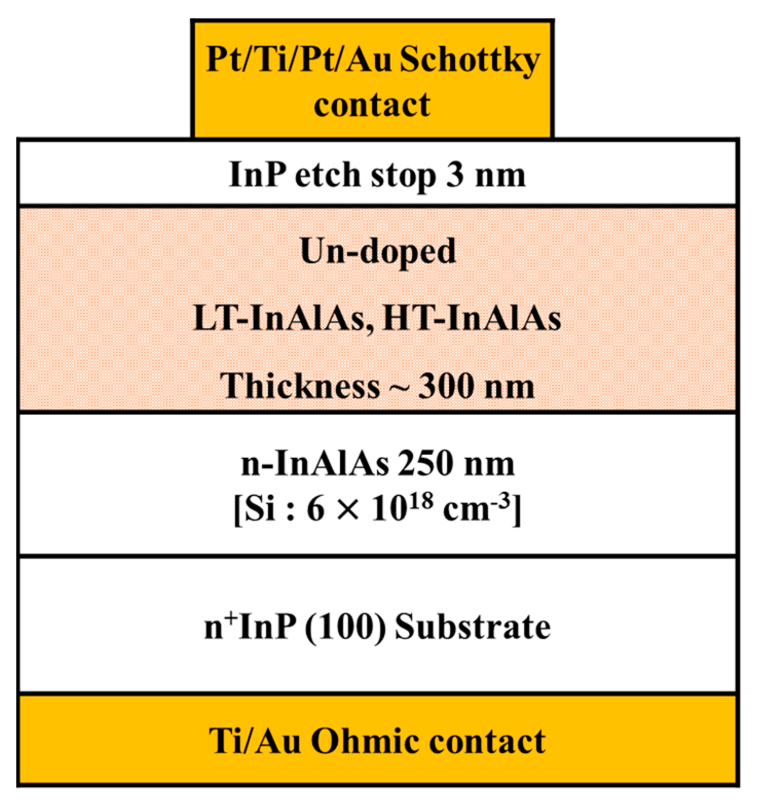



| Sample | Diode Area (cm−2) | SBH (eV) | Ideality Factor (n) | ||
|---|---|---|---|---|---|
| @ 77 K | @ 300 K | @ 77 K | @ 300 K | ||
| LT-InAlAs | 4.0 × 10⁻⁴ | 0.10 | 0.47 | 13.1 | 3.35 |
| HT-InAlAs | 0.16 | 0.71 | 5.72 | 1.17 | |
Publisher’s Note: MDPI stays neutral with regard to jurisdictional claims in published maps and institutional affiliations. |
© 2022 by the authors. Licensee MDPI, Basel, Switzerland. This article is an open access article distributed under the terms and conditions of the Creative Commons Attribution (CC BY) license (https://creativecommons.org/licenses/by/4.0/).
Share and Cite
Lee, S.-T.; Kong, M.; Jang, H.; Song, C.-H.; Kim, S.; Yun, D.-Y.; Jeong, H.-s.; Kim, D.-H.; Shin, C.-S.; Seo, K.-S. The Variation of Schottky Barrier Height Induced by the Phase Separation of InAlAs Layers on InP HEMT Devices. Crystals 2022, 12, 966. https://doi.org/10.3390/cryst12070966
Lee S-T, Kong M, Jang H, Song C-H, Kim S, Yun D-Y, Jeong H-s, Kim D-H, Shin C-S, Seo K-S. The Variation of Schottky Barrier Height Induced by the Phase Separation of InAlAs Layers on InP HEMT Devices. Crystals. 2022; 12(7):966. https://doi.org/10.3390/cryst12070966
Chicago/Turabian StyleLee, Sang-Tae, Minwoo Kong, Hyunchul Jang, Chang-Hun Song, Shinkeun Kim, Do-Young Yun, Hyeon-seok Jeong, Dae-Hyun Kim, Chan-Soo Shin, and Kwang-Seok Seo. 2022. "The Variation of Schottky Barrier Height Induced by the Phase Separation of InAlAs Layers on InP HEMT Devices" Crystals 12, no. 7: 966. https://doi.org/10.3390/cryst12070966
APA StyleLee, S.-T., Kong, M., Jang, H., Song, C.-H., Kim, S., Yun, D.-Y., Jeong, H.-s., Kim, D.-H., Shin, C.-S., & Seo, K.-S. (2022). The Variation of Schottky Barrier Height Induced by the Phase Separation of InAlAs Layers on InP HEMT Devices. Crystals, 12(7), 966. https://doi.org/10.3390/cryst12070966