

Demonstration of Acceptor-Like Traps at Positive Polarization Interfaces in Ga-Polar P-type (AlGaN/AlN)/GaN Superlattices


Abstract
1. Introduction
2. Materials and Methods
3. Results
4. Discussion
5. Conclusions
Author Contributions
Funding
Institutional Review Board Statement
Informed Consent Statement
Data Availability Statement
Conflicts of Interest
References
- Amano, H.; Baines, Y.; Beam, E.; Borga, M.; Bouchet, T.; Chalker, P.R.; Charles, M.; Chen, K.J.; Chowdhury, N.; Chu, R.; et al. The 2018 GaN Power Electronics Roadmap. J. Phys. D Appl. Phys. 2018, 51, 163001. [Google Scholar] [CrossRef] [Scilit]
- Baker, M.; Jain, S.; Shadmand, M.B. GaN Based High Frequency Power Electronic Interfaces: Challenges, Opportunities, and Research Roadmap. In Proceedings of the 2021 IEEE Power and Energy Conference at Illinois (PECI), San Diego, CA, USA, 1 April 2021; IEEE: Urbana, IL, USA, 2021; pp. 1–7. [Google Scholar]
- Chowdhury, S.; Swenson, B.L.; Wong, M.H.; Mishra, U.K. Current Status and Scope of Gallium Nitride-Based Vertical Transistors for High-Power Electronics Application. Semicond. Sci. Technol. 2013, 28, 074014. [Google Scholar] [CrossRef] [Scilit]
- Shrestha, P.; Guidry, M.; Romanczyk, B.; Karnaty, R.R.; Hatui, N.; Wurm, C.; Krishna, A.; Pasayat, S.S.; Keller, S.; Buckwalter, J.F.; et al. A Novel Concept Using Derivative Superposition at the Device-Level to Reduce Linearity Sensitivity to Bias in N-Polar GaN MISHEMT. In Proceedings of the 2020 Device Research Conference (DRC), Columbus, OH, USA, 21–24 June 2020; IEEE: Columbus, OH, USA, 2020; pp. 1–2. [Google Scholar] [CrossRef] [Scilit]
- Romanczyk, B.; Li, W.; Guidry, M.; Hatui, N.; Krishna, A.; Wurm, C.; Keller, S.; Mishra, U.K. N-Polar GaN-on-Sapphire Deep Recess HEMTs With High W-Band Power Density. IEEE Electron. Device Lett. 2020, 41, 1633–1636. [Google Scholar] [CrossRef] [Scilit]
- Romanczyk, B.; Zheng, X.; Guidry, M.; Li, H.; Hatui, N.; Wurm, C.; Krishna, A.; Ahmadi, E.; Keller, S.; Mishra, U.K. W-Band Power Performance of SiN-Passivated N-Polar GaN Deep Recess HEMTs. IEEE Electron. Device Lett. 2020, 41, 349–352. [Google Scholar] [CrossRef] [Scilit]
- Shrestha, P.; Guidry, M.; Romanczyk, B.; Hatui, N.; Wurm, C.; Krishna, A.; Pasayat, S.S.; Karnaty, R.R.; Keller, S.; Buckwalter, J.F.; et al. High Linearity and High Gain Performance of N-Polar GaN MIS-HEMT at 30 GHz. IEEE Electron. Device Lett. 2020, 41, 681–684. [Google Scholar] [CrossRef] [Scilit]
- Hatui, N.; Krishna, A.; Li, H.; Gupta, C.; Romanczyk, B.; Acker-James, D.; Ahmadi, E.; Keller, S.; Mishra, U.K. Ultra-High Silicon Doped N-Polar GaN Contact Layers Grown by Metal-Organic Chemical Vapor Deposition. Semicond. Sci. Technol. 2020, 35, 095002. [Google Scholar] [CrossRef] [Scilit]
- Sayed, I.; Liu, W.; Georgieva, J.; Krishna, A.; Keller, S.; Mishra, U.K. Characterization of AlSiO Dielectrics with Varying Silicon Composition for N-Polar GaN-Based Devices. Semicond. Sci. Technol. 2020, 35, 095027. [Google Scholar] [CrossRef] [Scilit]
- Ballestín-Fuertes, J.; Muñoz-Cruzado-Alba, J.; Sanz-Osorio, J.F.; Laporta-Puyal, E. Role of Wide Bandgap Materials in Power Electronics for Smart Grids Applications. Electronics 2021, 10, 677. [Google Scholar] [CrossRef] [Scilit]
- Nakamura, S.; Fasol, G. The Blue Laser Diode; Springer: Berlin, Heidelberg, 1997; ISBN 978-3-662-03464-4. [Google Scholar]
- Zhao, S.; Mi, Z. Recent Advances on P-Type III-Nitride Nanowires by Molecular Beam Epitaxy. Crystals 2017, 7, 268. [Google Scholar] [CrossRef] [Scilit]
- Asif Khan, M.; Shatalov, M.; Maruska, H.P.; Wang, H.M.; Kuokstis, E. III–Nitride UV Devices. Jpn. J. Appl. Phys. 2005, 44, 7191–7206. [Google Scholar] [CrossRef] [Scilit]
- Dahal, R.; Pantha, B.; Li, J.; Lin, J.Y.; Jiang, H.X. InGaN/GaN Multiple Quantum Well Solar Cells with Long Operating Wavelengths. Appl. Phys. Lett. 2009, 94, 063505. [Google Scholar] [CrossRef] [Scilit]
- Hurwitz, E.N.; Asghar, M.; Melton, A.; Kucukgok, B.; Su, L.; Orocz, M.; Jamil, M.; Lu, N.; Ferguson, I.T. Thermopower Study of GaN-Based Materials for Next-Generation Thermoelectric Devices and Applications. J. Electron. Mater. 2011, 40, 513–517. [Google Scholar] [CrossRef] [Scilit]
- Huang, Y.; Melton, A.; Jampana, B.; Jamil, M.; Ryou, J.-H.; Dupuis, R.D.; Ferguson, I.T. Compositional Instability in Strained InGaN Epitaxial Layers Induced by Kinetic Effects. J. Appl. Phys. 2011, 110, 064908. [Google Scholar] [CrossRef] [Scilit]
- Chatzakis, I.; Krishna, A.; Culbertson, J.; Sharac, N.; Giles, A.J.; Spencer, M.G.; Caldwell, J.D. Strong Confinement of Optical Fields Using Localized Surface Phonon Polaritons in Cubic Boron Nitride. Opt. Lett. 2018, 43, 2177. [Google Scholar] [CrossRef] [Scilit]
- Fragkos, I.E.; Tansu, N. Surface Plasmon Coupling in GaN: Eu Light Emitters with Metal-Nitrides. Sci. Rep. 2018, 8, 13365. [Google Scholar] [CrossRef] [Scilit]
- Zhou, C.; Ghods, A.; Saravade, V.G.; Patel, P.V.; Yunghans, K.L.; Ferguson, C.; Feng, Y.; Kucukgok, B.; Lu, N.; Ferguson, I.T. Review—The Current and Emerging Applications of the III-Nitrides. ECS J. Solid State Sci. Technol. 2017, 6, Q149. [Google Scholar] [CrossRef] [Scilit]
- Kako, S.; Santori, C.; Hoshino, K.; Götzinger, S.; Yamamoto, Y.; Arakawa, Y. A Gallium Nitride Single-Photon Source Operating at 200 K. Nat. Mater. 2006, 5, 887–892. [Google Scholar] [CrossRef] [Scilit]
- Quay, R. Gallium Nitride Electronics; Springer Series in Materials Science; Springer: Berlin, Germany, 2008; ISBN 978-3-540-71890-1. [Google Scholar]
- Hatui, N.; Krishna, A.; Pasayat, S.S.; Keller, S.; Mishra, U.K. Metal Organic Vapor Phase Epitaxy of Thick N-Polar InGaN Films. Electronics 2021, 10, 1182. [Google Scholar] [CrossRef] [Scilit]
- Chu, R.; Cao, Y.; Chen, M.; Li, R.; Zehnder, D. An Experimental Demonstration of GaN CMOS Technology. IEEE Electron. Device Lett. 2016, 37, 269–271. [Google Scholar] [CrossRef] [Scilit]
- Bader, S.J.; Chaudhuri, R.; Nomoto, K.; Hickman, A.; Chen, Z.; Then, H.W.; Muller, D.A.; Xing, H.G.; Jena, D. Gate-Recessed E-Mode p-Channel HFET With High On-Current Based on GaN/AlN 2D Hole Gas. IEEE Electron. Device Lett. 2018, 39, 1848–1851. [Google Scholar] [CrossRef] [Scilit]
- Arakawa, Y.; Ueno, K.; Kobayashi, A.; Ohta, J.; Fujioka, H. High Hole Mobility P-Type GaN with Low Residual Hydrogen Concentration Prepared by Pulsed Sputtering. APL Mater. 2016, 4, 086103. [Google Scholar] [CrossRef] [Scilit]
- Chowdhury, N.; Xie, Q.; Yuan, M.; Cheng, K.; Then, H.W.; Palacios, T. Regrowth-Free GaN-Based Complementary Logic on a Si Substrate. IEEE Electron. Device Lett. 2020, 41, 820–823. [Google Scholar] [CrossRef] [Scilit]
- Krishna, A.; Raj, A.; Hatui, N.; Koksaldi, O.; Jang, R.; Keller, S.; Mishra, U.K. AlGaN/GaN Superlattice-Based P-Type Field-Effect Transistor with Tetramethylammonium Hydroxide Treatment. Phys. Status Solidi A 2020, 217, 1900692. [Google Scholar] [CrossRef] [Scilit]
- Raj, A.; Krishna, A.; Hatui, N.; Gupta, C.; Jang, R.; Keller, S.; Mishra, U.K. Demonstration of a GaN/AlGaN Superlattice-Based p-Channel FinFET With High ON-Current. IEEE Electron. Device Lett. 2020, 41, 220–223. [Google Scholar] [CrossRef] [Scilit]
- Pampili, P.; Parbrook, P.J. Doping of III-Nitride Materials. Mater. Sci. Semicond. Process. 2017, 62, 180–191. [Google Scholar] [CrossRef] [Scilit]
- Kozodoy, P.; Smorchkova, Y.P.; Hansen, M.; Xing, H.; DenBaars, S.P.; Mishra, U.K.; Saxler, A.W.; Perrin, R.; Mitchel, W.C. Polarization-Enhanced Mg Doping of AlGaN/GaN Superlattices. Appl. Phys. Lett. 1999, 75, 2444–2446. [Google Scholar] [CrossRef] [Scilit]
- Raj, A.; Krishna, A.; Hatui, N.; Romanczyk, B.; Wurm, C.; Guidry, M.; Hamwey, R.; Pakala, N.; Keller, S.; Mishra, U.K. GaN/AlGaN Superlattice Based E-Mode p-Channel MES-FinFET with Regrown Contacts and >50 MA/Mm on-Current. In Proceedings of the 2021 IEEE International Electron Devices Meeting (IEDM), San Francisco, CA, USA, 11 December 2021; IEEE: San Francisco, CA, USA, 2021; pp. 5.4.1–5.4.4. [Google Scholar] [CrossRef] [Scilit]
- Krishna, A.; Raj, A.; Hatui, N.; Sayed, I.; Keller, S.; Mishra, U.K. Proposed Existence of Acceptor-like Traps at Positive Polarization Interfaces in p-Type III-Nitride Semiconductors. Appl. Phys. Lett. 2020, 117, 042104. [Google Scholar] [CrossRef] [Scilit]
- Krishna, A.; Raj, A.; Hatui, N.; Keller, S.; Denbaars, S.; Mishra, U.K. Acceptor Traps as the Source of Holes in P-Type N-Polar GaN/(AlN/AlGaN) Superlattices. Appl. Phys. Lett. 2022, 120, 132104. [Google Scholar] [CrossRef] [Scilit]
- Krishna, A.; Raj, A.; Hatui, N.; Keller, S.; Mishra, U.K. Investigation of Nitrogen Polar P-Type Doped GaN/AlxGa(1-x)N Superlattices for Applications in Wide-Bandgap p-Type Field Effect Transistors. Appl. Phys. Lett. 2019, 115, 172105. [Google Scholar] [CrossRef] [Scilit]
- Lund, C.; Agarwal, A.; Romanczyk, B.; Mates, T.; Nakamura, S.; DenBaars, S.P.; Mishra, U.K.; Keller, S. Investigation of Mg δ -Doping for Low Resistance N-Polar p-GaN Films Grown at Reduced Temperatures by MOCVD. Semicond. Sci. Technol. 2018, 33, 095014. [Google Scholar] [CrossRef] [Scilit]
- Fichtenbaum, N.A.; Mates, T.E.; Keller, S.; DenBaars, S.P.; Mishra, U.K. Impurity Incorporation in Heteroepitaxial N-Face and Ga-Face GaN Films Grown by Metalorganic Chemical Vapor Deposition. J. Cryst. Growth 2008, 310, 1124–1131. [Google Scholar] [CrossRef] [Scilit]
- Prozheeva, V.; Makkonen, I.; Li, H.; Keller, S.; Mishra, U.K.; Tuomisto, F. Interfacial N Vacancies in Ga N/(Al, Ga) N/Ga N Heterostructures. Phys. Rev. Appl. 2020, 13, 044034. [Google Scholar] [CrossRef] [Scilit]
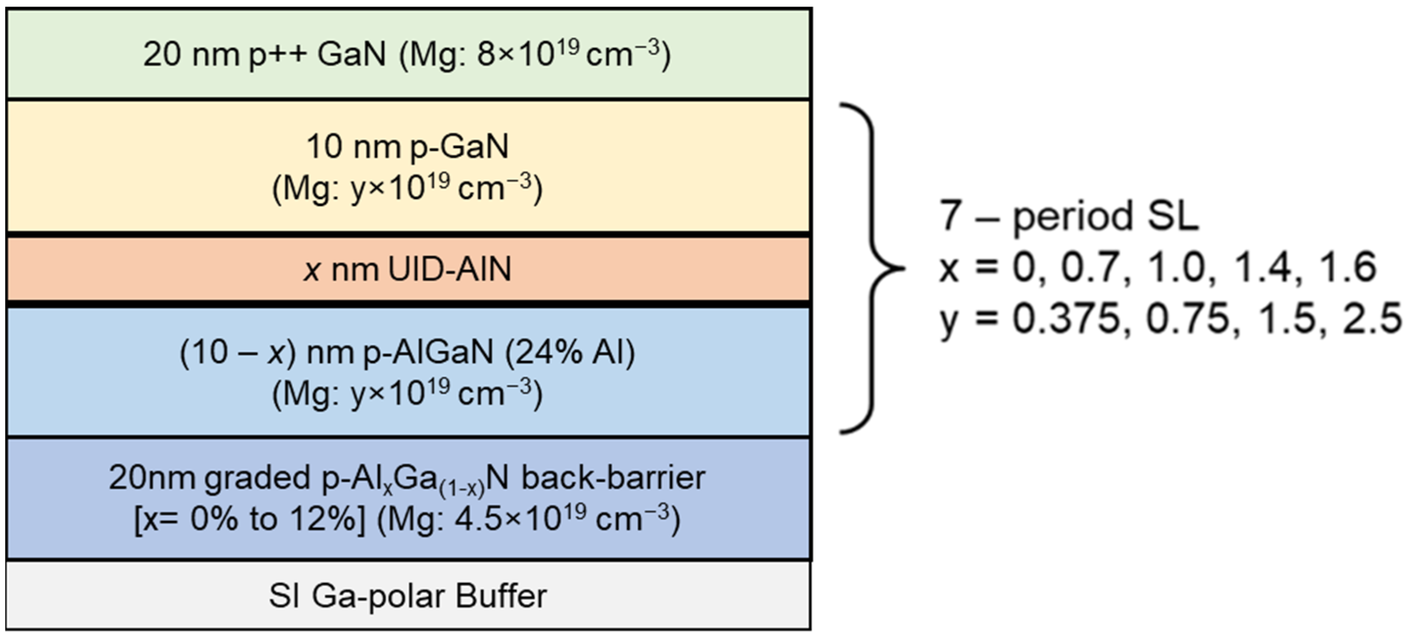
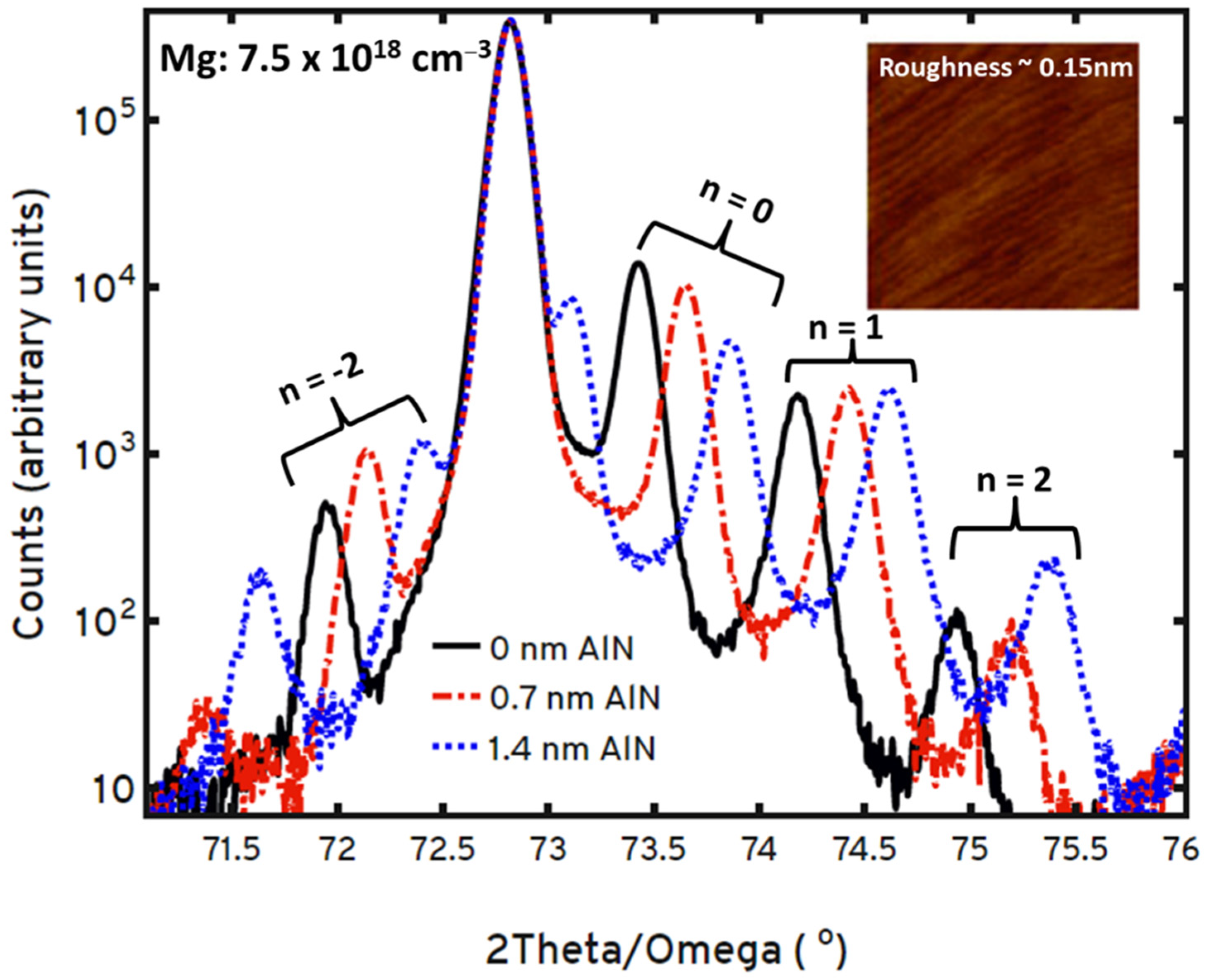
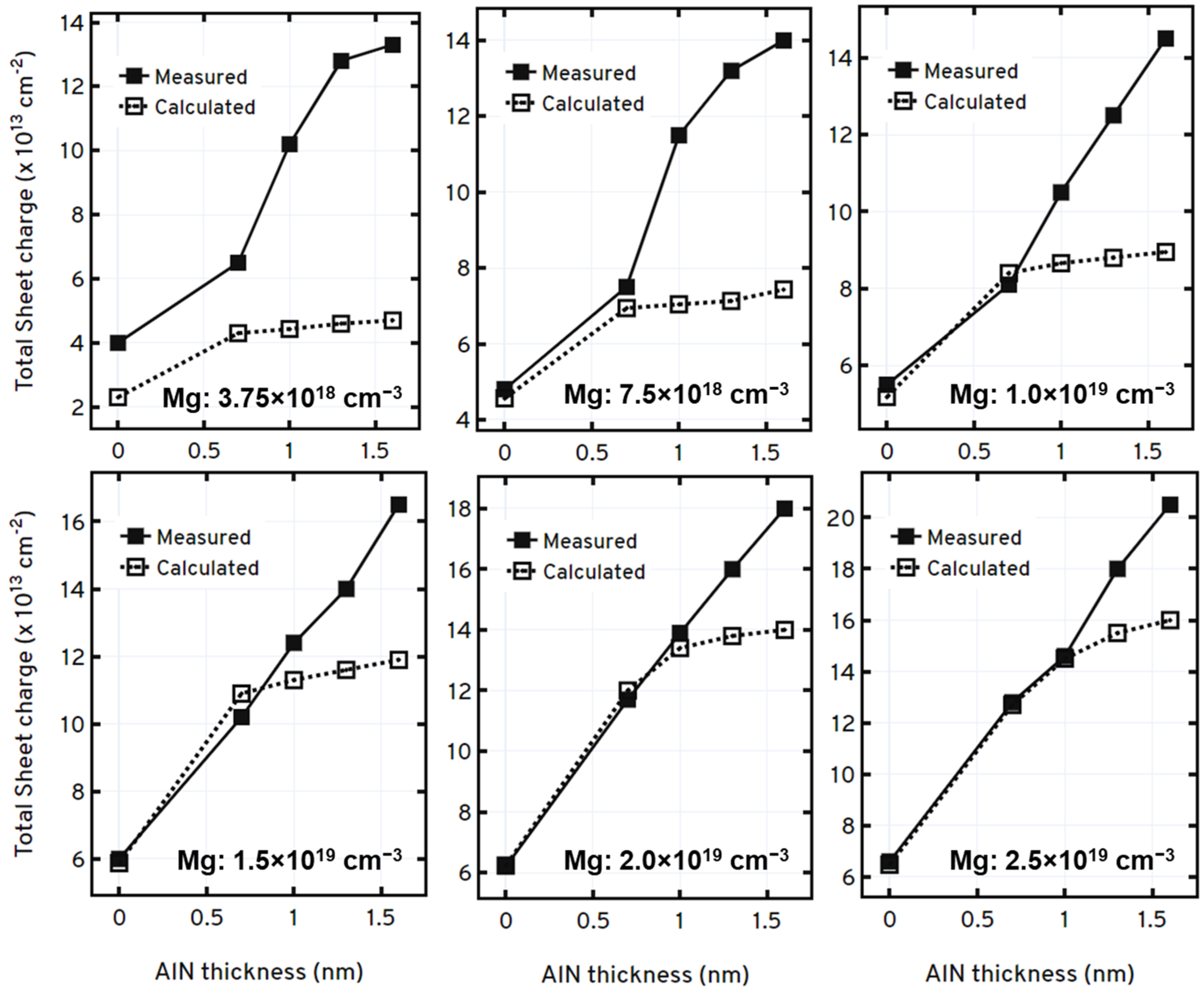

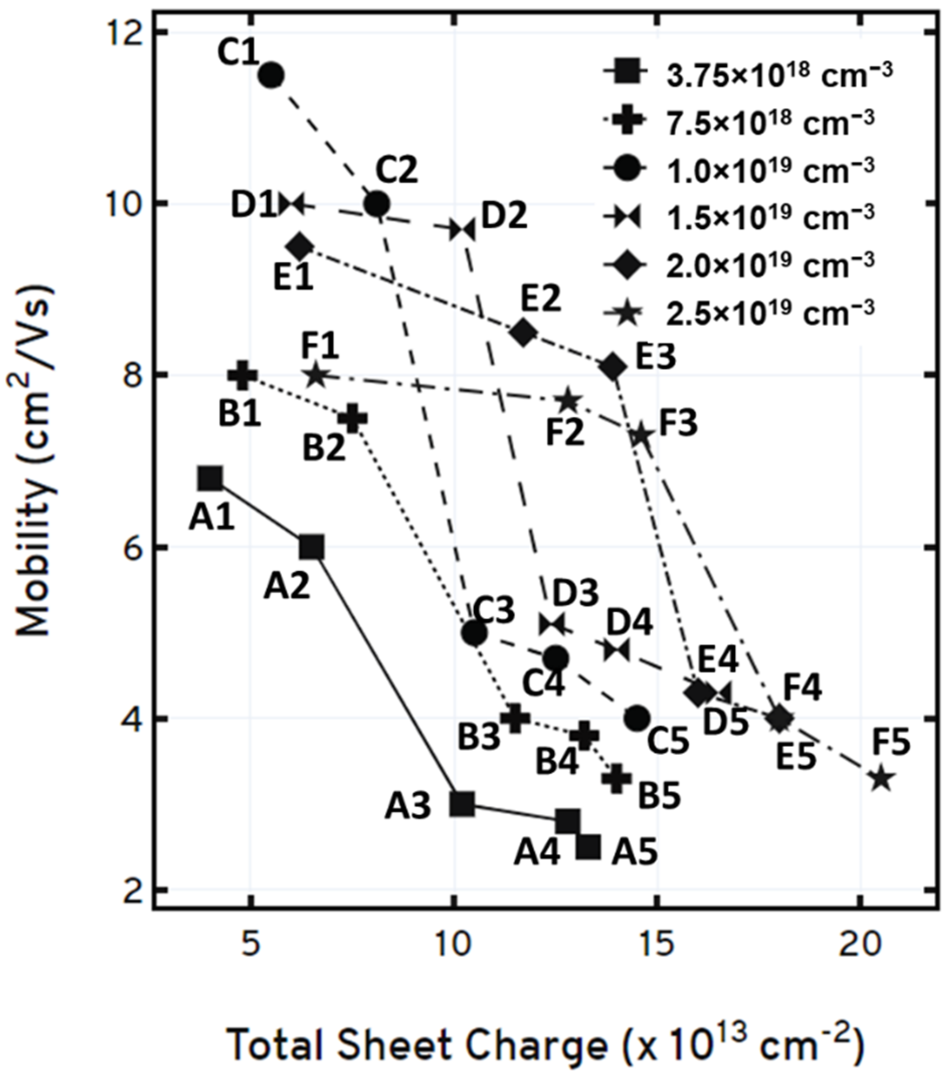
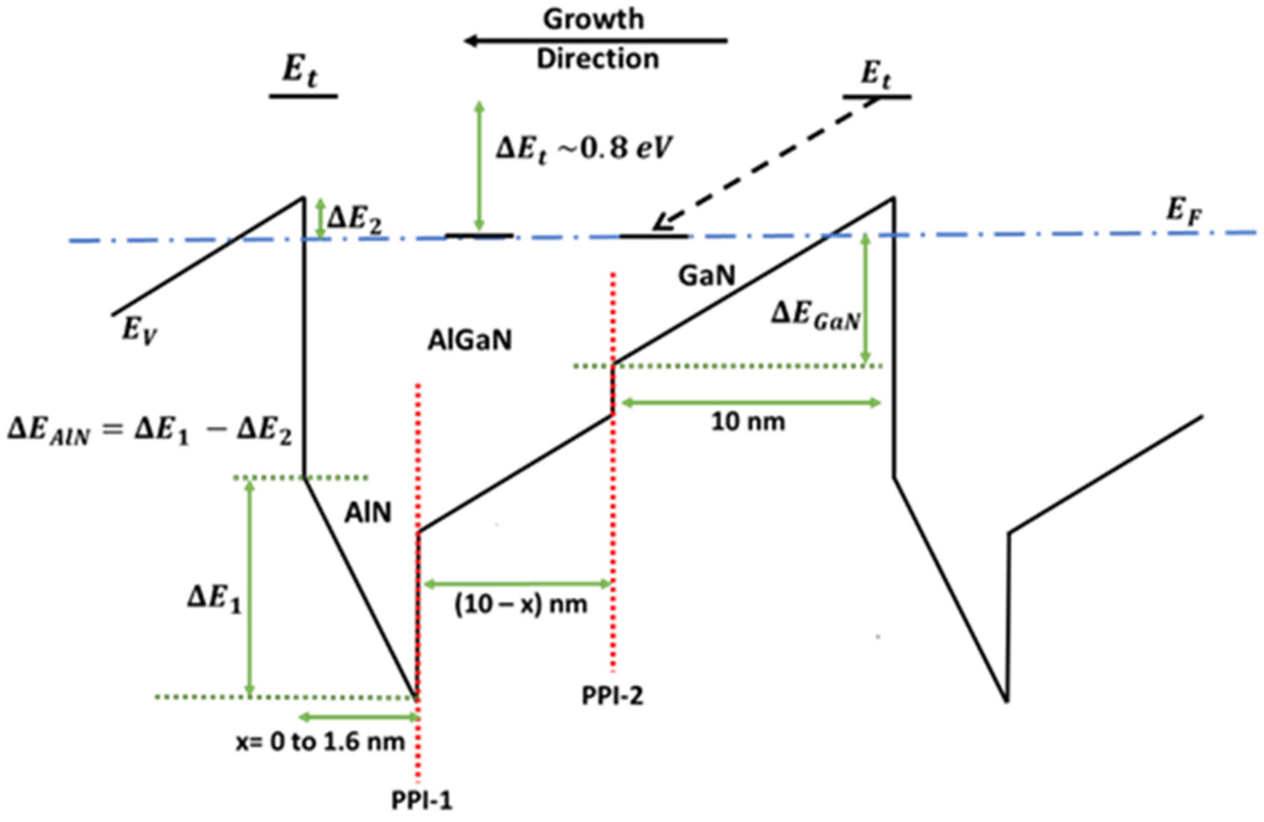
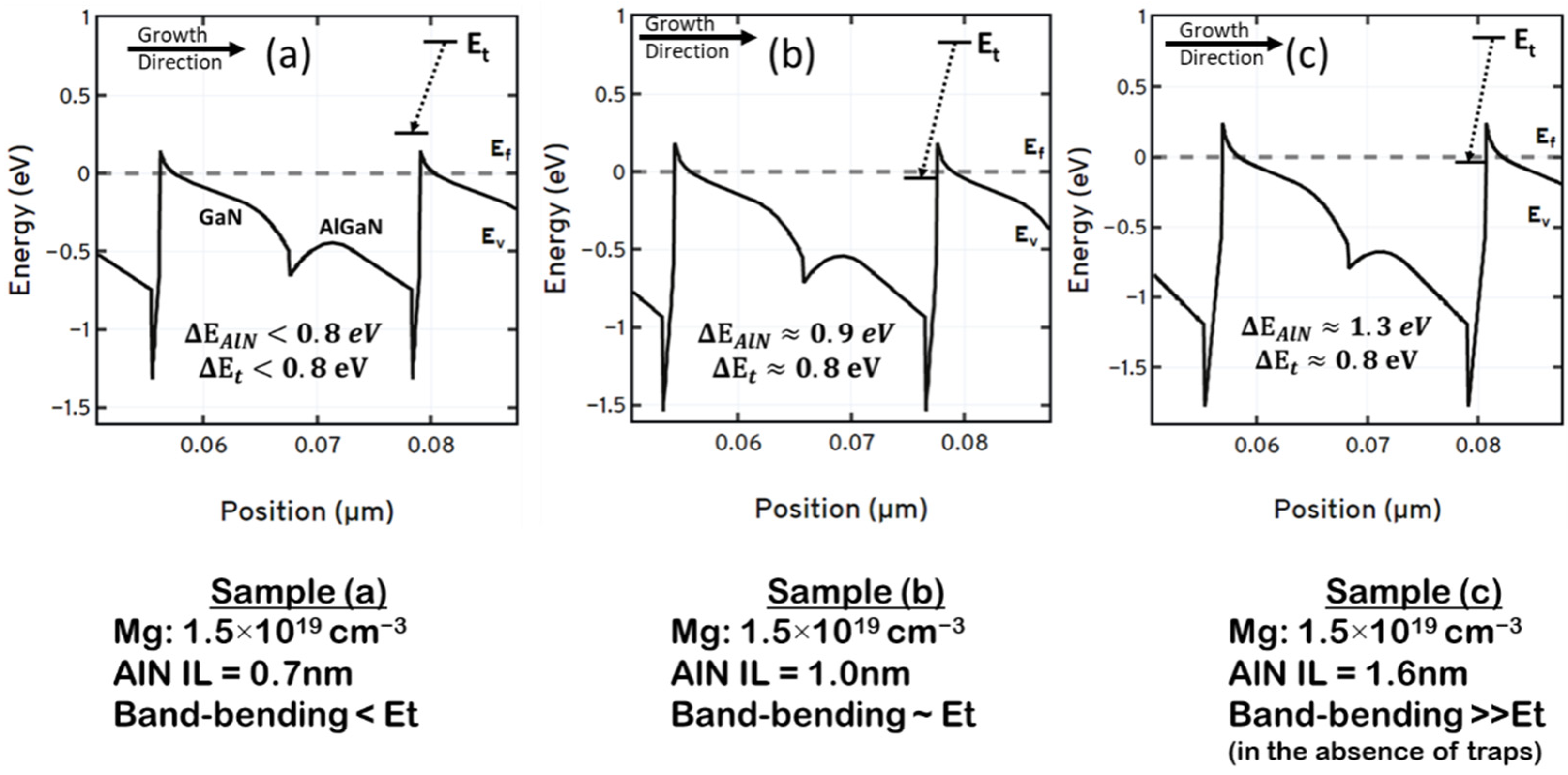

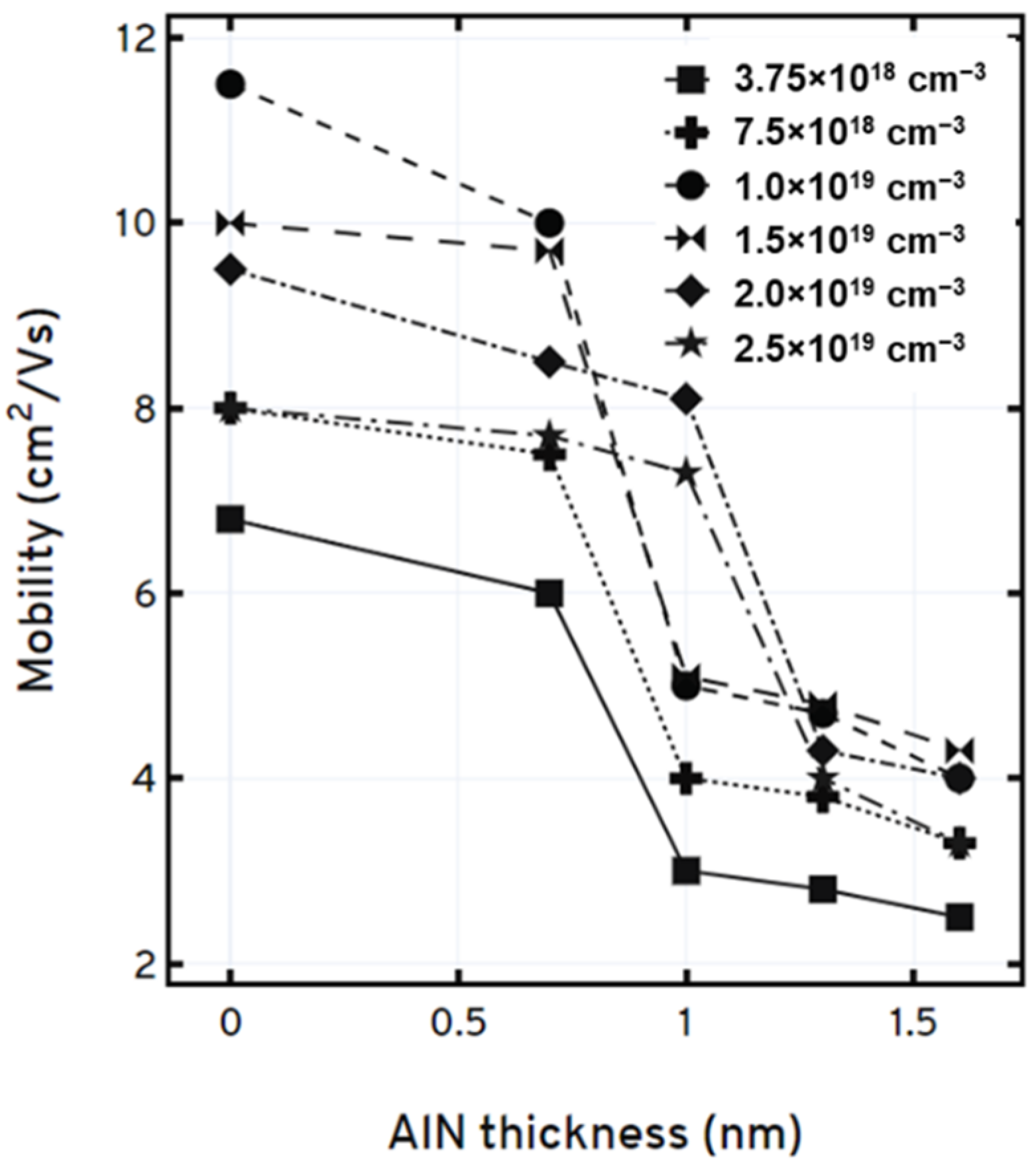
| Sample No. | Doping (×1018 cm−3) | AlN Layer Thickness (nm) | Traps at PPI-1 (Defined in Figure 6) | Traps at PPI-2 (Defined in Figure 6) | Effect of Traps on Mobility? |
|---|---|---|---|---|---|
| A-1 | 3.75 | 0 | Un-ionized | Ionized | No |
| A-2 | 3.75 | 0.7 | Un-ionized | Ionized | No |
| A-3 | 3.75 | 1.0 | Ionized | Ionized | Yes |
| A-4 | 3.75 | 1.4 | Ionized | Ionized | Yes |
| A-5 | 3.75 | 1.6 | Ionized | Ionized | Yes |
| B-1 | 7.5 | 0 | Un-ionized | Un-ionized | - |
| B-2 | 7.5 | 0.7 | Un-ionized | Ionized | No |
| B-3 | 7.5 | 1.0 | Ionized | Ionized | Yes |
| B-4 | 7.5 | 1.4 | Ionized | Ionized | Yes |
| B-5 | 7.5 | 1.6 | Ionized | Ionized | Yes |
| C-1 | 10 | 0 | Un-ionized | Un-ionized | - |
| C-2 | 10 | 0.7 | Un-ionized | Un-ionized | - |
| C-3 | 10 | 1.0 | Ionized | Ionized | Yes |
| C-4 | 10 | 1.4 | Ionized | Ionized | Yes |
| C-5 | 10 | 1.6 | Ionized | Ionized | Yes |
| D-1 | 15 | 0 | Un-ionized | Un-ionized | - |
| D-2 | 15 | 0.7 | Un-ionized | Un-ionized | - |
| D-3 | 15 | 1.0 | Ionized | Un-ionized | Yes |
| D-4 | 15 | 1.4 | Ionized | Ionized | Yes |
| D-5 | 15 | 1.6 | Ionized | Ionized | Yes |
| E-1 | 20 | 0 | Un-ionized | Un-ionized | - |
| E-2 | 20 | 0.7 | Un-ionized | Un-ionized | - |
| E-3 | 20 | 1.0 | Un-ionized | Un-ionized | - |
| E-4 | 20 | 1.4 | Ionized | Un-ionized | Yes |
| E-5 | 20 | 1.6 | Ionized | Ionized | Yes |
| F-1 | 25 | 0 | Un-ionized | Un-ionized | - |
| F-2 | 25 | 0.7 | Un-ionized | Un-ionized | - |
| F-3 | 25 | 1.0 | Un-ionized | Un-ionized | - |
| F-4 | 25 | 1.4 | Ionized | Un-ionized | Yes |
| F-5 | 25 | 1.6 | Ionized | Un-ionized | Yes |
Publisher’s Note: MDPI stays neutral with regard to jurisdictional claims in published maps and institutional affiliations. |
© 2022 by the authors. Licensee MDPI, Basel, Switzerland. This article is an open access article distributed under the terms and conditions of the Creative Commons Attribution (CC BY) license (https://creativecommons.org/licenses/by/4.0/).
Share and Cite
Krishna, A.; Raj, A.; Hatui, N.; Keller, S.; Mishra, U.K. Demonstration of Acceptor-Like Traps at Positive Polarization Interfaces in Ga-Polar P-type (AlGaN/AlN)/GaN Superlattices. Crystals 2022, 12, 784. https://doi.org/10.3390/cryst12060784
Krishna A, Raj A, Hatui N, Keller S, Mishra UK. Demonstration of Acceptor-Like Traps at Positive Polarization Interfaces in Ga-Polar P-type (AlGaN/AlN)/GaN Superlattices. Crystals. 2022; 12(6):784. https://doi.org/10.3390/cryst12060784
Chicago/Turabian StyleKrishna, Athith, Aditya Raj, Nirupam Hatui, Stacia Keller, and Umesh K. Mishra. 2022. "Demonstration of Acceptor-Like Traps at Positive Polarization Interfaces in Ga-Polar P-type (AlGaN/AlN)/GaN Superlattices" Crystals 12, no. 6: 784. https://doi.org/10.3390/cryst12060784
APA StyleKrishna, A., Raj, A., Hatui, N., Keller, S., & Mishra, U. K. (2022). Demonstration of Acceptor-Like Traps at Positive Polarization Interfaces in Ga-Polar P-type (AlGaN/AlN)/GaN Superlattices. Crystals, 12(6), 784. https://doi.org/10.3390/cryst12060784