Article

High Reflectivity AlN/Al1−xInxN Distributed Bragg Reflectors across the UV Regions by Sputtering

by
Ellen Serwaa Frimpong-Manso
and
Liancheng Wang
*
State Key Laboratory of High Performance Complex Manufacturing, College of Mechanical and Electrical Engineering, Central South University, Changsha 410083, China
*
Author to whom correspondence should be addressed.
Crystals 2022, 12(2), 162; https://doi.org/10.3390/cryst12020162
Submission received: 13 December 2021 / Revised: 31 December 2021 / Accepted: 8 January 2022 / Published: 24 January 2022

Abstract

:
To improve the performance of III-nitride compound semiconductor-based optoelectronic devices, highly reflective distributed Bragg reflectors (DBRs) are a requirement. In this report, AlN and Al1−xInxN layers were first sputtered and characterized concerning their optical, structural and morphological properties. Ellipsometry measurements were used to determine the optical constants (refractive index, n and coefficient of extinction, k, in dependence of the wavelengths of the layers. The indium content of the Al1−xInxN film was investigated by X-ray photoelectron spectroscopy analysis. Subsequently, AlN/Al1−xInxN DBRs with high reflectivity spectra operating in the UV A, B and C were designed and fabricated on Si (111) and SiO2 substrates by radio frequency (RF) magnetron sputtering. The DBRs consist of an eight-pair AlN/Al0.84In0.16N at 235 nm, 290 nm and 365 nm with reflectances of 86.5%, 97.7% and 97.5% with FWHM of 45 nm, 70 nm and 96 nm, respectively. Atomic force microscopy analysis yielded a Root Mean Square (RMS) of 2.95 nm, implying that the DBR samples can achieve reasonable smoothness over a wide area. Furthermore, the impact of an annealing phase, which is frequently required during device growth, was investigated. Our findings indicate that AlN and Al1−xInxN are suitable materials for the fabrication of deep UV DBRs.

1. Introduction

Researchers have become keenly interested in developing deep-ultraviolet (UV) III-nitride based resonant cavity light-emitting diodes (RCLEDs) and vertical surface-emitting cavity lasers (VCSELs) [1]. For this purpose, it is imperative to grow distributed Bragg reflectors (DBRs) based on III-nitride semiconductors in the UV region as a core component. Due to their ease of fabrication and controllable optical properties, DBRs have sparked considerable interest in photonic and optoelectrical applications such as wavelength filters, polarization splitters and high-reflection mirrors. They are especially useful in spacecraft design to provide solar radiation protection.
III-nitride semiconductors have many applications in optoelectronic and electronic technology. As a result of the strong bond between nitrogen and each group III atom, high thermal conductivity, high electron saturation velocity [2,3,4,5], and a variety of other properties, group III nitrides are among the most promising optoelectronic materials. They possess excellent intrinsic properties such as a wide range of direct transition-type energy bandgaps starting at 6.2 eV for AlN [6,7] and with the current revision of bandgap of InN from 1.9 eV to 0.7 eV, new avenues have been opened to researchers for the preparation of In-rich ternary alloys such as InGaN and InAlN which have potential applications in high efficiency light emitting diodes, solar cells, photodiodes operating in visible and ultraviolet (UV) regions and solar cells [8,9,10,11,12,13] along with other high power electronic devices.
AlN and GaN are the preferred materials for the realization of nitride-dependent DBRs due to their comparatively large refractive index contrast, Δ / n = 0.16 [14] and their ability to withstand high temperatures as a results of their high melting point. This is not to say that the aforementioned nitrides are without drawbacks. In order to curb the problem of large lattice-mismatch and other irregularities often associated with III-nitrides, Bhattacharyya and colleagues reported a high-reflectivity (more than 99%) and crack-free UV AlGaN/AlN DBRs on (0001) sapphire at 340 nm with 29.5 bilayers by plasma-assisted molecular beam epitaxy (MBE) [1]. Later, Carlin and Ilegems fabricated lattice matched InAlN/GaN heterostructures of excellent quality by metalorganic vapor phase epitaxy centered at 515 nm with over 90% reflectivity for 20 pairs [15]. Detchprohm et al. have also reported on AlGaN/AlN DBRs via metal–organic chemical vapor deposition (MOCVD) for peak reflectivity between 220 nm and 250 nm with reflectivity as high as 96–97% for 30.5 pairs of layers [16]. Despite these promising outcomes, the relatively low refractive index contrast between the constituent layers and thus requiring high numbers of DBR pairs to achieve high reflectivity and longer growth times is a big challenge. In contrast to molecular beam epitaxy (MBE) [17] and metal-organic chemical vapor deposition (MOCVD) [18,19] techniques which involves high temperatures, complex and hazardous processes, radio-frequency magnetron sputtering has the advantages of simple growth procedure, high deposition rate, ability to sputter any alloy or compound at low temperatures, low cost, and exceptionally high film adhesion. Recently, Qiang Li reported on the growth and characterization of hBN/BAlN DBRs for peak reflectivity of 52% (6 pairs) and 90% (9 pairs) at 280 nm and 300 nm, respectively, through RF-sputtering. Although these results are quite impressive, the quality of the BAlN material still needs to be improved and optimized [20].
In this work, we demonstrate the successful growth of crack-free, highly reflective DBRs across the UV spectrum, (UV A, B and C) and investigations of its temperature reliability.

2. Materials and Methods

2.1. Deposition of the AlN and AlInN Thin Films

Single layers of AlN and AlInN thin films were deposited on Si (111) substrates by radio frequency magnetron sputtering (conventional TRP-450 RF magnetron sputtering system) with aluminum and indium plates of 99.99% purity as the target materials to investigate the optical properties of these materials. Prior to the deposition, the substrates were cleaned using the well-known Radio Corporation of America (RCA) cleaning process. The radio frequency (RF) and direct current (DC) sputter power were 160 W and 25 W, respectively, and pressure in the chamber was evacuated to a background pressure of 4.0 × 10⁻⁴ Pa at a temperature of 150 °C. Argon (Ar) and nitrogen (N2) were then introduced into the chamber at flow rates of 20 sccm: 20 sccm during the deposition of the AIN layer and 10 sccm: 18 sccm during the deposition of the AlInN layer with a working pressure of 1.5 Pa. All targets were pre-sputtered for 10 min before the actual deposition and each layer was sputtered for 60 min.

2.2. Growth of the AlN/Al1−xInxN Distributed Bragg Reflectors (DBRs)

Subsequently, AlN/Al1−xInxN DBRs were sputtered. Quarter-wavelength AlN/Al1−xInxN DBRs were deposited on Si (111) and SiO2 substrates by the same magnetron sputtering technology. AlN as low and Al1−xInxN as high index material were chosen as an optimal alternating layer sequence. All the DBR samples were sputtered under the same growth conditions for the deposition of the thin films except for variations in growth times to influence the thickness. The thickness of each layer is given by; d = λ/4n, where λ = target wavelength, d = thickness needed for DBR with the target wavelength and n = refractive index at the target wavelength. To obtain AlN/Al1−xInxN DBRs with different operating wavelengths in the various UV regions, the sputter time was varied. The sputter times were 20 min, 26 min and 34 min for eight periods which yielded reflectances at 235 nm, 290 nm and 365 nm, respectively. The commercial finite-difference time domain (FDTD) method of an FDTD software package from Lumerical Inc. was used as the simulation tool to analyze the optical properties of the DBR structures. In the x-direction and y-direction, the period layers boundary condition was used. In the z-direction, perfectly matched layer boundary conditions were used. Ellipsometry measurements, X-ray photoelectron spectroscopy (XPS) analysis and high-resolution X-ray diffraction (HR-XRD) ω–2θ scans with Cu Kα radiation (0.15406 nm) were undertaken to characterize the thin films. For optical reflectivity measurements, a PG2000-PRO spectrophotometer with a resolution of 1.01 nm was employed. A UV Al mirror with certified reflectivity in the 200–1000 nm region was used as reference. Information on the surface morphology and structure were obtained from an Olympus BX51M optical-contrast microscope, atomic force microscopy (AFM) and a TESCAN MIRA3 LMU field-emission scanning electron microscope (FE-SEM). The refractive indices (n) and extinction coefficient (k) of the AlN and Al1−xInxN films were measured with a dual rotating-compensator Mueller matrix ellipsometer (ME-L ellipsometer, Wuhan Eoptics Technology Co., Wuhan, China). Thermal annealing processes were also performed with a GSL-1700X-S vacuum tube furnace in ambient air at various annealing temperatures of 400 °C and 500 °C for 40 and 50 min, respectively, to investigate the reliability of the DBR samples. The DBR samples were annealed to the aforementioned temperatures from room temperature, held isothermally for 5 min inside the chamber, and then allowed to cool down to room temperature.

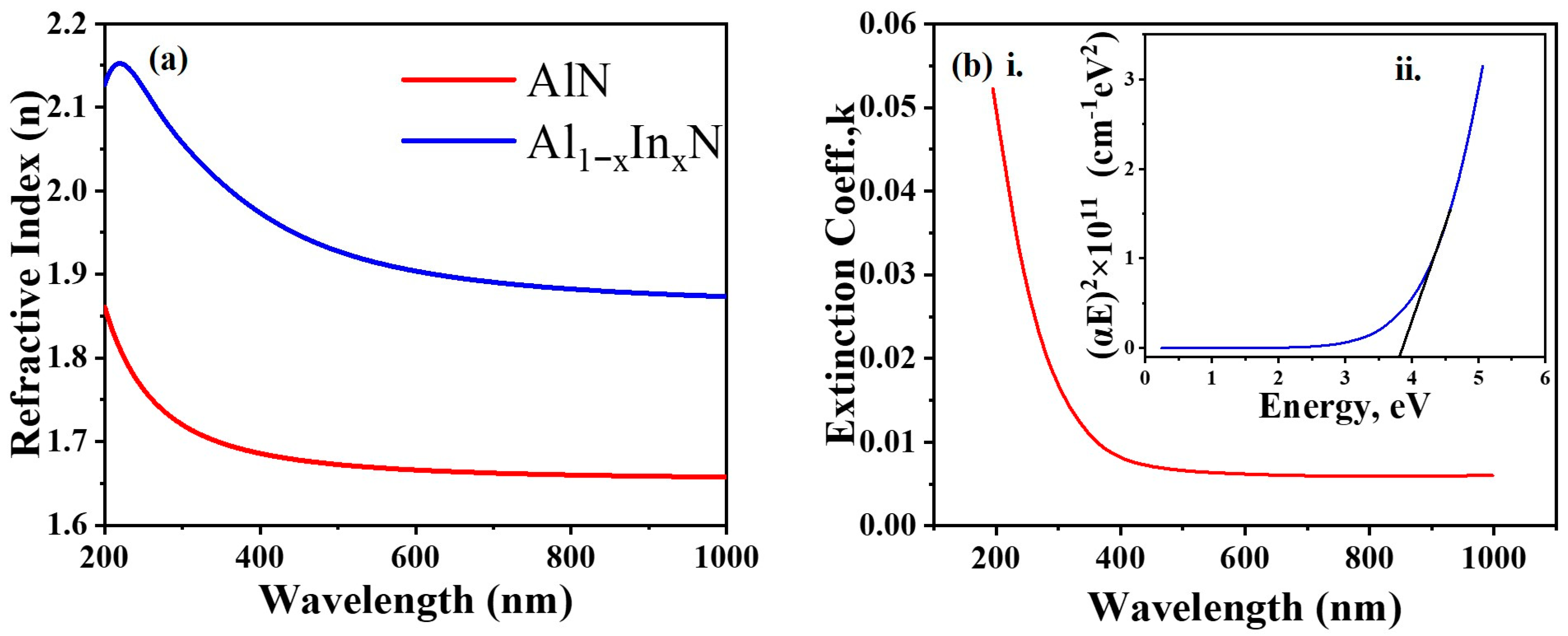
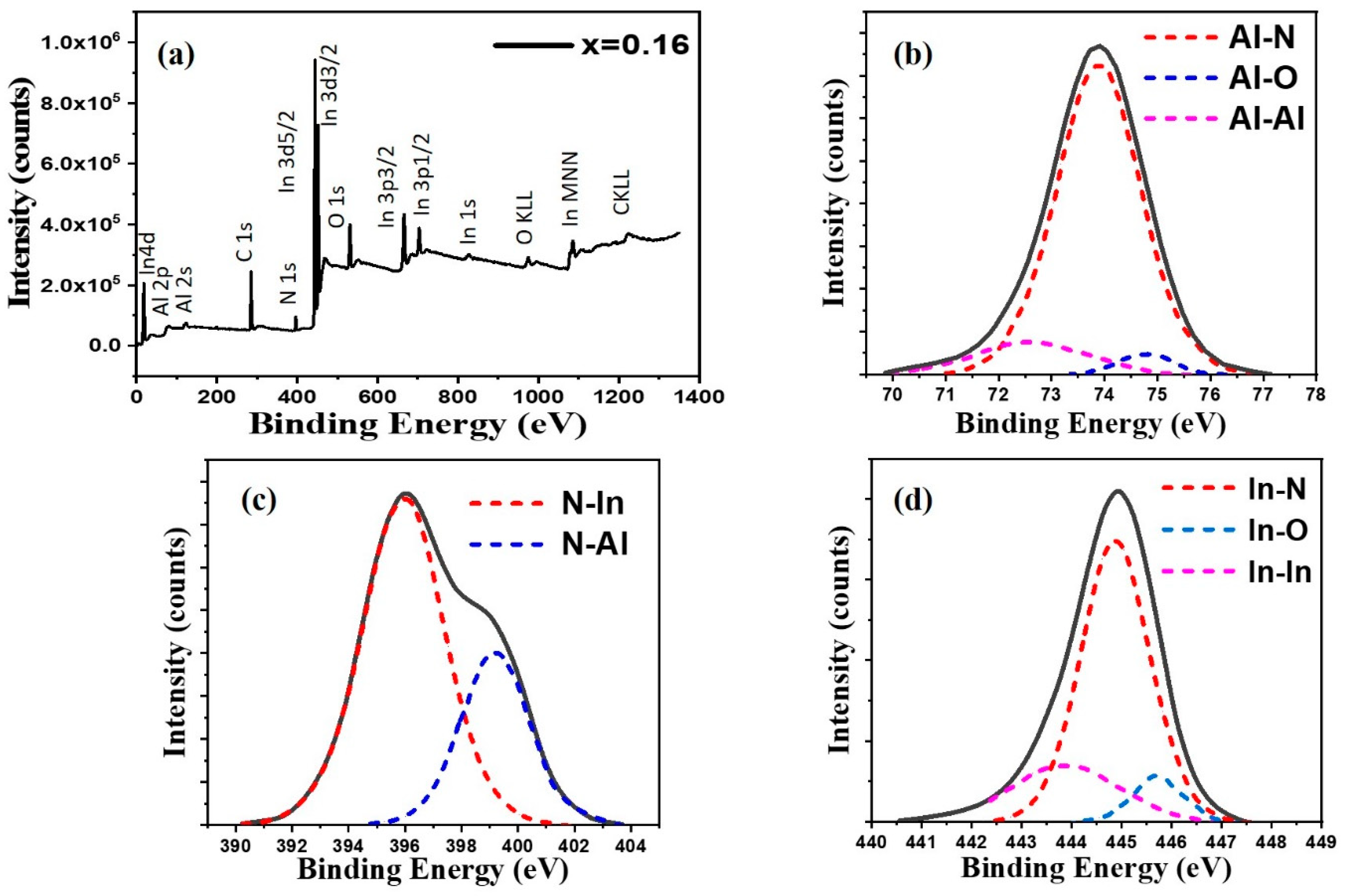
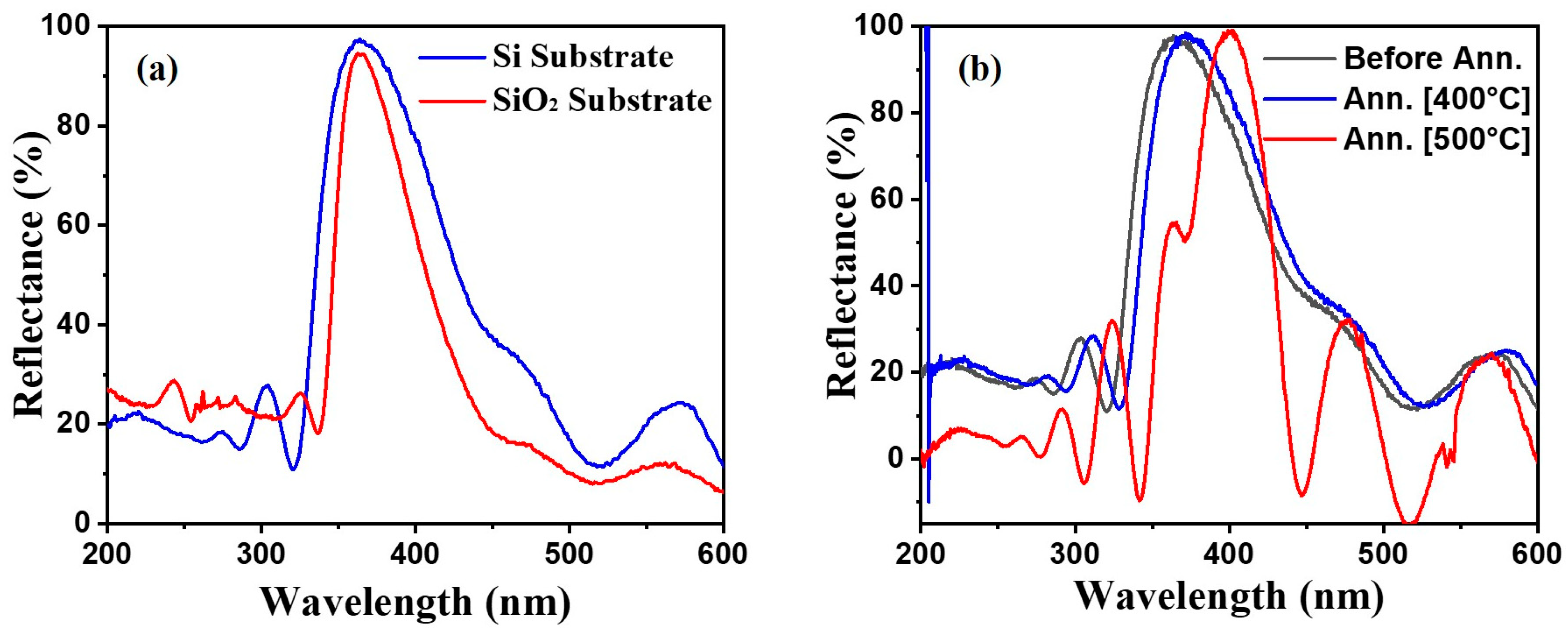
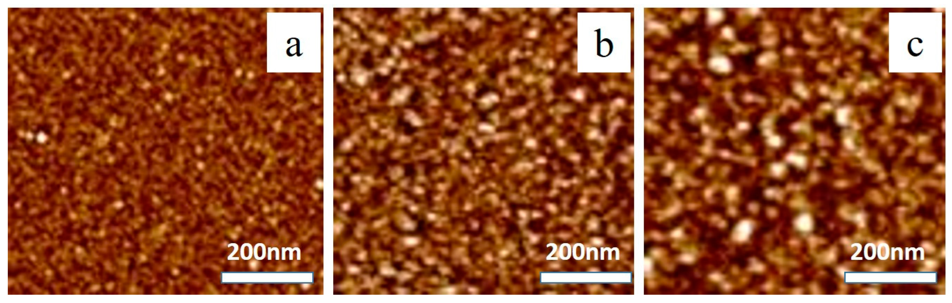
3. Results and Discussion

The refractive index of the AlN and Al1−xInxN thin films sputtered over a spectral range of 200–1000 nm is as shown in Figure 1a. At the target wavelengths, the refractive index contrast, Δn, between the AlN and Al1−xInxN films are 0.359 at 235 nm, 0.342 at 290 nm and 0.312 at 365 nm. The extended Tauc formula was used to calculate the bandgap energy, Eg, of AlInN layers:
( α E ) r E E g
from the extinction coefficient k, Figure 1b(i). The absorption coefficient can be obtained by; α = 4πk/λ, where λ is the target wavelength. The original Tauc formula is only applicable to amorphous layers in which the exponent is r = 1/2 [21]. In the case of semiconductors, absorption is inversely proportional to density of states hence, r = 2 [22]. Eg is the resultant of the intersection of the tangent of ( α E ) 2 with the energy axis (black line). The optical band gap is determined to be 3.8 eV as shown in the inset-II of Figure 1b, which is close to prior experimental data and theoretical calculations [23].
A typical 2θ/ω XRD scan of the Al1−xInxN observed in a broad range from 29° to 35° with a diffraction peak at 33.5° in the 2θ/ω scan is shown in Figure 2. No peaks were observed at the positions expected for pure InN 0002 at 31.33° and for pure AlN 0002 at 36.14°. This indicates that the Al1−xInxN layer obtained has a wurtzite structure and is highly c-axis oriented with the AlInN crystal aligned normally to the substrate surface.
Figure 3a represents the full XPS spectra and (b–d) the deconvoluted survey of the AlInN film elemental composition. The Al2p, In3d and N1s peaks from the XPS survey were fractionated to see how the atoms bond in the film. As a binding energy reference, the primary C1s peak for adventitious surface carbon was set at 284.6 eV [24]. The spectrum shows peaks of considerable intensity located at 73.9 eV, 444.8 eV, 531.4 eV, 396.1 eV and 284.6 eV; corresponding to Al2p, In3d5/2, O1s, N1s, C 1s and binding energies, respectively. The elemental content of Al, C, O, In and N is 24.5%, 22.2%, 7.9%, 4.8% and 40.5%, respectively. The data confirm the presence of substantial amounts of oxygen and carbon which may be probably due to contamination of the sample. The Al and In content are also calculated to be 84% and 16% respectively. Figure 3b–d are the high-resolution spectra for the In3d5/2, Al2p, and N1s signals for the Al0.84In0.16N film. The peak corresponding to the Al2p level was deconvoluted into three Gaussian functions as shown in Figure 3b. Two of the sub peaks were centered on the binding energies: 74.8 eV and 72.6 eV, which correspond to the Al–O and Al–Al bonds. The minor bump shows the energy of the third component at 73.9 eV, which can be attributed to the Al–N bond. Figure 3c illustrates that indium’s spectrum, In3d5/2, has three peaks at 445.8 eV, 444.8 eV, and 443.7 eV, which corresponds to the In–O, In–N and In–In bonds, respectively. The N1s core-level photoelectron spectra deconvoluted into two main sub peaks of 396.1 eV and 399.3 eV in Figure 3d are attributed to the N–In and N–Al bonds, respectively, confirming the alloy state and formation of Al0.84In0.16N film.
The parameters of the DBR structures we investigated are summarized in Table 1. The reflectance of the DBR is primarily dependent on the refractive index contrast (Δn = nHnL) of the AlN and Al1−xInxN alternating layers and the number of periods (N). As a result of high refractive index contrast between the AlN and Al0.84In0.16N films, highly reflective DBRs can be theoretically and experimentally achieved in the various UV regions. Figure 4a illustrates the peak reflectance obtained for 86.5% (blue solid—experimental) with a full width half maximum (FWHM) of ~45 nm and 89.2% (dash-simulation) at 235 nm (UV C); 97.7% (green solid-experimental) with a FWHM of ~70 nm and 98.1% (dash-simulation) at 290 nm (UV B); and 97.5% (red solid-experimental) with a FWHM of ~96 nm and 97.8% (dash-simulation) at 365 nm (UV A). From the results obtained, it can be noted that the refractive index contrast decreases with an increase in the wavelength and consequently, a reduction in reflectivity (in the case of the UV B and A respectively). This tends to differ with the UV C DBR, even though the highest refractive index contrast is achieved at 235 nm, it does not translate into its reflectance. This could be attributed to abnormal absorption in the deep UV bands which has resulted in the decrease in its reflectance, rendering the DBR at 235 nm having the lowest reflectance even though it has the biggest refractive index contrast. The reflectivity spectra of the experiment and simulation for AlN/Al0.84In0.16N DBRs show good agreement in terms of the positions of the spectrum. However, the stopband of the simulation spectra is slightly narrower than in the experimental results. This might arise from discrepancies in refractive index contrast in the actual deposition and the simulation when taking into account the optical loss from material absorption and interface scattering. Figure 4b shows the SEM image of the eight-pair AlN/Al1−xInxN DBR structure. The lighter layers represent the AlN and the darker layers represent the AlInN. The mean thickness of the AlN and AlInN layers estimated from the SEM image are 53 nm/46 nm, 42 nm/34 nm and 32 nm/26 nm operating at 365 nm, 290 nm and 235 nm, respectively. These figures are in good agreement with that measured from the simulation (54 nm/45 nm, 42 nm/35 nm and 33 nm/27 nm). In general, the AlN/AlInN interfaces are well defined and flat as shown in Figure 4b. The interface between AlN and AlInN is, however, not clear enough. This may be due to the low surface migration mobility of Al atoms and surface segregation of indium atoms during growth which can result in a thin intermixing of Al-rich and In-segregation regions, as well as phase separation and other defects at the interface [25]. When depositing AlInN materials with a high Al content, such imperfect, blurry interfaces are easily formed.
The top view image of the as-prepared AlN/AlInN DBR observed with an optical microscope is illustrated in Figure 5a. The image demonstrates that no cracks were discovered on the DBR surface. Figure 5b depicts a typical AFM image obtained by scanning a 3 μm × 3 μm region with an RMS of 2.95 nm, implying that the DBR sample can achieve reasonable smoothness over a wide area.
Due to the flexibility associated with sputtering technique, nitride DBRs can be deposited on different substrates. Figure 6a represents the reflectance spectra of the UV A DBR (365 nm) deposited on Si and SiO2 substrates with the same deposition parameters. There were slight changes in the spectra with the peak reflectance on the Si substrate exhibiting a higher reflectivity and broader FWHM; 97.5% with 96 nm than that on the SiO2 substrate; 94.1% with 64 nm. This could be attributed to the high reflectance of Si substrates stemming from the lower lattice parameter mismatch between the wurtzite nitride structure and the silicon in contrast to the SiO2 substrate. To investigate the reliability of the DBR, thermal annealing processes were performed in ambient air at temperatures of 400 °C and 500 °C. Figure 6b illustrates the reflectance spectra of the DBR before and after annealing in air. The annealed DBR has an increment in reflectivity and wavelength. For the annealed DBR at 400 °C, it was observed that the stop band red-shifts (7 nm) had an increased reflectance of 98.3% (0.8% enhancement) at 372 nm with a FWHM of 94 nm. At 500 °C, the peak reflectance increased to 99.1% (1.6% enhancement) at a wavelength of 402 nm (37 nm red-shift) with a FWHM of 70 nm. Such increments could be the result of an increase in the refractive index contrast between the AlN and AlInN layers. During the fabrication of the DBR, the AlN and AlInN layers are deposited at a relatively low temperature (150 °C) which may render a non-uniformity in the distribution of indium. Hence, there may be nitrogen- and oxygen-related defects in the films. Nonetheless, the indium atom may have redistributed when the sample was annealed, thereby improving the DBR quality and consequently, the reflectance. This is similar to DBRs fabricated in the visible [26] and infrared regions [27].
As seen in the AFM image in Figure 7a–c, the granular structure of the DBR as grown appears to be more compact than the DBR annealed at 400 °C and 500 °C. There is also evidence of little grains clumping together to form larger grains. The grain size of the DBR before annealing is the smallest. The surface roughness of the three DBR samples is measured to 2.95 ± 0.15 nm.
A summary of the key parameters obtained in this study is listed in Table 2. Compared to prior works reported on other nitride-based DBRs, the AlInN/AlN DBR features the highest reflectivity by using only eight periods with a much smaller thickness and as such makes it a better candidate for the design and fabrication of deep UV DBRs.

4. Conclusions

In summary, we have presented the fabrication and characterization of AlN/AlInN stacks-based Bragg reflectors by RF magnetron sputtering. Ellipsometry measurements for the refractive index and coefficient of extinction of the AlN and AlInN layers were determined. The AlN/AlInN DBRs with high reflectivity were then experimentally demonstrated in the UV A region with a peak wavelength of 365 nm (92.3%), UV B region centered at 295 nm (92.8%) and UV C, 240 (94.8%). AFM images confirm that the DBR samples can achieve reasonable smoothness over a wide area. The optical microscopic image and cross-sectional SEM results reveal no cracks and good structural quality with well-defined interfaces. The DBR reliability was investigated by annealing in air at high temperatures. Our results indicate that the reflectivity of the DBR can be enhanced by annealing. The fabrication of high-performance optoelectronic devices such as LEDs, VCSELs, and RC-LEDs could benefit from these crack-free AlN/AlInN UV DBRs with broad FWHM and high reflectivity.

Author Contributions

Conceptualization, L.W.; formal analysis, E.S.F.-M.; investigation, E.S.F.-M.; data curation, E.S.F.-M.; writing—original draft preparation, E.S.F.-M.; writing—review and editing, E.S.F.-M. and L.W.; supervision, L.W.; funding acquisition, L.W. All authors have read and agreed to the published version of the manuscript.

Funding

Key Laboratory of Energy Conversion and Storage Technologies (Southern University of Science and Technology), Ministry of Education, Shenzhen, China; Project of State Key Laboratory of High-Performance Complex Manufacturing, Central South University, No. ZZYJKT2021-11.

Institutional Review Board Statement

Not applicable.

Informed Consent Statement

Not applicable.

Data Availability Statement

Not applicable.

Conflicts of Interest

The authors declare no conflict of interest.

References

  1. Bhattacharyya, A.; Iyer, S.; Iliopoulos, E.; Sampath, A.; Cabalu, J.; Moustakas, T.; Friel, I. High reflectivity and crack-free AlGaN/AlN ultraviolet distributed Bragg reflectors. J. Vac. Sci. Technol. B Microelectron. Nanometer Struct. Processing Meas. Phenom. 2002, 20, 1229–1233. [Google Scholar] [CrossRef]
  2. Davydov, V.Y.; Klochikhin, A.; Seisyan, R.; Emtsev, V.; Ivanov, S.; Bechstedt, F.; Furthmüller, J.; Harima, H.; Mudryi, A.; Aderhold, J. Absorption and emission of hexagonal InN. Evidence of narrow fundamental band gap. Phys. Status Solidi (B) 2002, 229, r1–r3. [Google Scholar] [CrossRef]
  3. Nakamura, S.; Senoh, M.; Nagahama, S.-I.; Iwasa, N.; Yamada, T.; Matsushita, T.; Kiyoku, H.; Sugimoto, Y. InGaN-based multi-quantum-well-structure laser diodes. Jpn. J. Appl. Phys. 1996, 35, L74. [Google Scholar] [CrossRef]
  4. Rubio, A.; Corkill, J.L.; Cohen, M.L.; Shirley, E.L.; Louie, S.G. Quasiparticle band structure of AlN and GaN. Phys. Rev. B 1993, 48, 11810. [Google Scholar] [CrossRef]
  5. Wright, A.F.; Nelson, J. Explicit treatment of the gallium 3d electrons in GaN using the plane-wave pseudopotential method. Phys. Rev. B 1994, 50, 2159. [Google Scholar] [CrossRef]
  6. Yim, W.; Stofko, E.; Zanzucchi, P.; Pankove, J.; Ettenberg, M.; Gilbert, S. Epitaxially grown AlN and its optical band gap. J. Appl. Phys. 1973, 44, 292–296. [Google Scholar] [CrossRef]
  7. Shen, L.; Cheng, T.; Wu, L.; Li, X.; Cui, Q. Synthesis and optical properties of aluminum nitride nanowires prepared by arc discharge method. J. Alloys Compd. 2008, 465, 562–566. [Google Scholar] [CrossRef]
  8. Davydov, V.Y.; Klochikhin, A.; Seisyan, R.; Emtsev, V.; Ivanov, S.; Bechstedt, F.J.; Furthmüller, H.; Harima, A.V.; Mudryi, J.; Aderhold, O.; et al. Graul. Phys. Status Solidi B 2002, 229, R1. [Google Scholar] [CrossRef]
  9. Rivera, C.; Pau, J.; Pereiro, J.; Muñoz, E. Properties of Schottky barrier photodiodes based on InGaN/GaN MQW structures. Superlattices Microstruct. 2004, 36, 849–857. [Google Scholar] [CrossRef]
  10. Chen, Z.; Sakai, Y.; Zhang, J.; Egawa, T.; Wu, J.; Miyake, H.; Hiramatsu, K. Effect of strain on quantum efficiency of InAlN-based solar-blind photodiodes. Appl. Phys. Lett. 2009, 95, 083504. [Google Scholar] [CrossRef]
  11. Gardner, N.; Müller, G.; Shen, Y.; Chen, G.; Watanabe, S.; Götz, W.; Krames, M. Blue-emitting InGaN–GaN double-heterostructure light-emitting diodes reaching maximum quantum efficiency above 200 A/cm2. Appl. Phys. Lett. 2007, 91, 243506. [Google Scholar] [CrossRef]
  12. Zhou, S.; Liu, X.; Yan, H.; Chen, Z.; Liu, Y.; Liu, S. Highly efficient GaN-based high-power flip-chip light-emitting diodes. Opt. Express 2019, 27, A669–A692. [Google Scholar] [CrossRef]
  13. Zhou, S.; Zheng, C.; Lv, J.; Gao, Y.; Wang, R.; Liu, S. GaN-based flip-chip LEDs with highly reflective ITO/DBR p-type and via hole-based n-type contacts for enhanced current spreading and light extraction. Opt. Laser Technol. 2017, 92, 95–100. [Google Scholar] [CrossRef] [Green Version]
  14. Ive, T.; Brandt, O.; Kostial, H.; Hesjedal, T.; Ramsteiner, M.; Ploog, K.H. Crack-free and conductive Si-doped AlN/GaN distributed Bragg reflectors grown on 6H-SiC (0001). Appl. Phys. Lett. 2004, 85, 1970–1972. [Google Scholar] [CrossRef] [Green Version]
  15. Carlin, J.-F.; Ilegems, M. High-quality AlInN for high index contrast Bragg mirrors lattice matched to GaN. Appl. Phys. Lett. 2003, 83, 668–670. [Google Scholar] [CrossRef]
  16. Detchprohm, T.; Liu, Y.-S.; Mehta, K.; Wang, S.; Xie, H.; Kao, T.-T.; Shen, S.-C.; Yoder, P.D.; Ponce, F.A.; Dupuis, R.D. Sub 250 nm deep-UV AlGaN/AlN distributed Bragg reflectors. Appl. Phys. Lett. 2017, 110, 011105. [Google Scholar] [CrossRef] [Green Version]
  17. Adolph, D.; Zamani, R.R.; Dick, K.A.; Ive, T. Hybrid ZnO/GaN distributed Bragg reflectors grown by plasma-assisted molecular beam epitaxy. APL Mater. 2016, 4, 086106. [Google Scholar] [CrossRef] [Green Version]
  18. Carlin, J.-F.; Dorsaz, J.; Feltin, E.; Butté, R.; Grandjean, N.; Ilegems, M.; Laügt, M. Crack-free fully epitaxial nitride microcavity using highly reflective AlInN/GaN Bragg mirrors. Appl. Phys. Lett. 2005, 86, 031107. [Google Scholar] [CrossRef]
  19. Kruse, C.; Dartsch, H.; Aschenbrenner, T.; Figge, S.; Hommel, D. Growth and characterization of nitride-based distributed Bragg reflectors. Phys. Status Solidi (B) 2011, 248, 1748–1755. [Google Scholar] [CrossRef]
  20. Li, Q.; Zhang, Q.; Bai, Y.; Zhang, H.; Hu, P.; Li, Y.; Yun, F. Deep-UV hexagonal boron nitride (hBN)/BAlN distributed Bragg reflectors fabricated by RF-sputtering. Opt. Mater. Express 2021, 11, 180–188. [Google Scholar] [CrossRef]
  21. Tauc, J.; Grigorovici, R.; Vancu, A. Optical properties and electronic structure of amorphous germanium. Phys. Status Solidi (B) 1966, 15, 627–637. [Google Scholar] [CrossRef]
  22. Pankove, J. Transitions between band tails. In Optical Processes in Semiconductors; Dover: New York, NY, USA, 1975; pp. 43–46. [Google Scholar]
  23. Aschenbrenner, T.; Dartsch, H.; Kruse, C.; Anastasescu, M.; Stoica, M.; Gartner, M.; Pretorius, A.; Rosenauer, A.; Wagner, T.; Hommel, D. Optical and structural characterization of AlInN layers for optoelectronic applications. J. Appl. Phys. 2010, 108, 063533. [Google Scholar] [CrossRef]
  24. Wei, G.; Goto, Y.; Ohta, A.; Makihara, K.; Murakami, H.; Higashi, S.; Miyazaki, S. Handbook of X-ray Photoelectron Spectroscopy: A Reference Book of Standard Spectra for the Identification and Interpretation of XPS Data Handbook of X-ray Photoelectron Spectroscopy: A Reference Book of Standard Spectra for the Identification and Interpretation of XPS Data 240, 1993. IEICE Trans. Electron. 2011, 94, 699–704. [Google Scholar]
  25. Minj, A.; Cavalcoli, D.; Cavallini, A. Indium segregation in AlInN/AlN/GaN heterostructures. Appl. Phys. Lett. 2010, 97, 132114. [Google Scholar] [CrossRef]
  26. Yang, X.; Xiao, H.; Cao, D.; Zhao, C.; Shen, L.; Ma, J. Fabrication, annealing, and regrowth of wafer-scale nanoporous GaN distributed Bragg reflectors. Scr. Mater. 2018, 156, 10–13. [Google Scholar] [CrossRef]
  27. Feng, I.-W.; Jin, S.; Li, J.; Lin, J.; Jiang, H. SiO2/TiO2 distributed Bragg reflector near 1.5 μm fabricated by e-beam evaporation. J. Vac. Sci. Technol. A Vac. Surf. Film. 2013, 31, 061514. [Google Scholar] [CrossRef]
  28. Feltin, E.; Carlin, J.-F.; Dorsaz, J.; Christmann, G.; Butté, R.; Laügt, M.; Ilegems, M.; Grandjean, N. Crack-free highly reflective AlInN/AlGaN Bragg mirrors for UV applications. Appl. Phys. Lett. 2006, 88, 051108. [Google Scholar] [CrossRef]
  29. Moudakir, T.; Gautier, S.; Suresh, S.; Abid, M.; El Gmili, Y.; Patriarche, G.; Pantzas, K.; Troadec, D.; Jacquet, J.; Genty, F. Suppression of crack generation in AlGaN/GaN distributed Bragg reflectors grown by MOVPE. J. Cryst. Growth 2013, 370, 12–15. [Google Scholar] [CrossRef]
Figure 1. (a) Refractive index of the AlN and Al1−xInxN layer (b) i. Coefficient of extinction of Al1−xInxN, ii. Band gap of Al1−xInxN.
Crystals 12 00162 g001
Figure 2. X-ray diffraction (XRD) pattern of the AlInN film.
Crystals 12 00162 g002
Figure 3. (a) Full X-ray photoelectron spectroscopy (XPS) spectra (bd) deconvoluted high-resolution spectra of the Al1−xInxN.
Crystals 12 00162 g003
Figure 4. (a) Experimental reflectance spectra of the DBR samples in the ultraviolet (UV) A, B and C regions (solid) with their corresponding simulation reflectance (dash); (b) scanning electron microscopy (SEM) micrographs of the AlN/AlInN DBR.
Crystals 12 00162 g004
Figure 5. (a) Optical microscopy image and (b) atomic force microscopy (AFM) view of the AlN/AlInN DBR.
Crystals 12 00162 g005
Figure 6. (a) Reflectance spectra of the UV A DBR on Si and SiO2 substrate. (b) Reflectance spectra of the UV A DBR before (black) and after annealing at 400 °C (blue) and 500 °C (red).
Crystals 12 00162 g006
Figure 7. AFM images of the DBR samples: (a) as grown (b) annealed at 400 °C and (c) annealed at 500 °C.
Crystals 12 00162 g007
Table 1. Summary of the distributed Bragg reflector (DBR) structures’ parameters.
DBR 1DBR 2DBR3
Low index layerAlNAlNAlN
High index layerAl0.84In0.16NAl0.84In0.16NAl0.84In0.16N
Target Wavelength235 nm290 nm365 nm
No. of bilayers888
Sputter Time20 min26 min34 min
Deposition temp.150 °C150 °C150 °C
Simulation layer thickness (nm)dAlN = 26dAlN = 42dAlN = 53
dAlInN = 32dAlInN = 34dAlInN = 46
Table 2. Key parameters obtained in this work compared to prior works.
MaterialFabrication MethodPeriodWavelength (nm)Thickness (High Index Material)Thickness (Low Index Material) Total ThicknessReflectance (%)Ref.
AlGaN/AlNMBE29.534035 nm39.5 nm219899[1]
AlInN/AlGaNMOCVD3534332 nm36 nm238099.5[28]
AlGaN/AlNMOCVD30.5220–250--2196–237997[16]
AlGaN/GaNMOCVD2038436 nm42 nm156090[29]
AlInN/AlNR.F Sputtering8235, 290,36526 nm/34 nm/45 nm32 nm/42 nm/54 nm464, 608, 79286.5, 97.7, 97.5This work
Publisher’s Note: MDPI stays neutral with regard to jurisdictional claims in published maps and institutional affiliations.

