1. Introduction
Graphene has been widely studied by scholars for its special electrical and optical properties. All kinds of novel ideas were proposed for the design of optical, electrical, and mechanical devices based on monolayer graphene by taking advantage of its properties, such as the perfect absorption of optoelectronic device, optical communication system and industrial production [
1,
2,
3,
4,
5,
6]. Meanwhile, Li et al. provided a comprehensive review of graphene synthesis methods and its potential industrial implementations [
7]; the literature data indicated that a large amount of high-quality graphene can be synthesised by oxidative exfoliation–reduction, liquid-phase exfoliation (LPE) and chemical vapor deposition (CVD), which lays the foundation for the commercial application of graphene.
However, graphene has an absorption of only about 2.3% in the infrared to visible spectral range of incident light on the surface [
8,
9], which seriously obstructs the application range and performance of graphene-based devices. Accordingly, it is necessary to increase light–matter interactions of graphene to improve the absorptance of graphene. Thus, the researchers have proposed a variety of structures such as multilayer thin film photonic crystal (PC) by using the photonic local state formed between graphene and PC to improve the absorptance of graphene [
10,
11,
12,
13]. For instance, Gao et al. proposed a visible full-band optical wave absorber using graphene and 1D-PC composite structure, and a full-band absorptance of the visible optical band can reach 0.88 [
9]. Wu et al. proposed a 1D graphene-based multilayer structure that comprised traditional dielectric material and graphene; the absorptance of the structure was maintained higher than 80% [
14]. Castriota et al. studied the optical properties of a monolayer Chemical Vapor Deposition (CVD)- grown graphene (transferred from a copper substrate onto SiO2/Si) by means of Variable Angle Spectroscopic Ellipsometry (VASE), and the estimated carrier density from optical conductivity data reached 7.8 × 10
13cm
2 [
15]. Those studies bring inspiration for the design of graphene-based optoelectronic devices. For the general periodic PC structure, when studying the transmission, reflection and absorption of light and the gain and loss of the medium are often not considered or the loss of the medium is regarded as an adverse factor; however, for optical structures that satisfy parity–time (PT) symmetry, quantum dots are anthropogenically introduced into the substrate medium, forming gain and loss dielectric layers. When the gain and loss dielectric layers are accurately anastomotic, a bizarre optical transmission phenomenon can be produced under the action of external pump energy [
16,
17,
18], and the graphene layer can be transferred to a PT symmetry PC structure to improve graphene absorptance using the method described in the literature [
15].
Therefore, in this paper, taking graphene as the top layer and 1D-PC with PT-symmetry structure as the bottom layer, an optical micro-cavity has been established by combining graphene and PT-symmety PC multilayer stacks. By optimizing the structure’s parameters, the absorption of graphene at the typical communication wavelength of 1550 nm can be enormously enhanced. Meanwhile, based on the electro-optic effect of LiNbO3 crystal, graphene absorption can be modulated regularly by modulated electric fields. In this manner, the in-phase and out-phase enhanced absorption of graphene can be realized. The proposed design exhibits ultrastrong and modulable light absorption compared with the traditional 1D-PC structure and the complex 1D-PC with special material layer. These findings have certain reference significance for the design of tunable absorbers, photodetectors, optical communication devices and related optoelectronic devices.
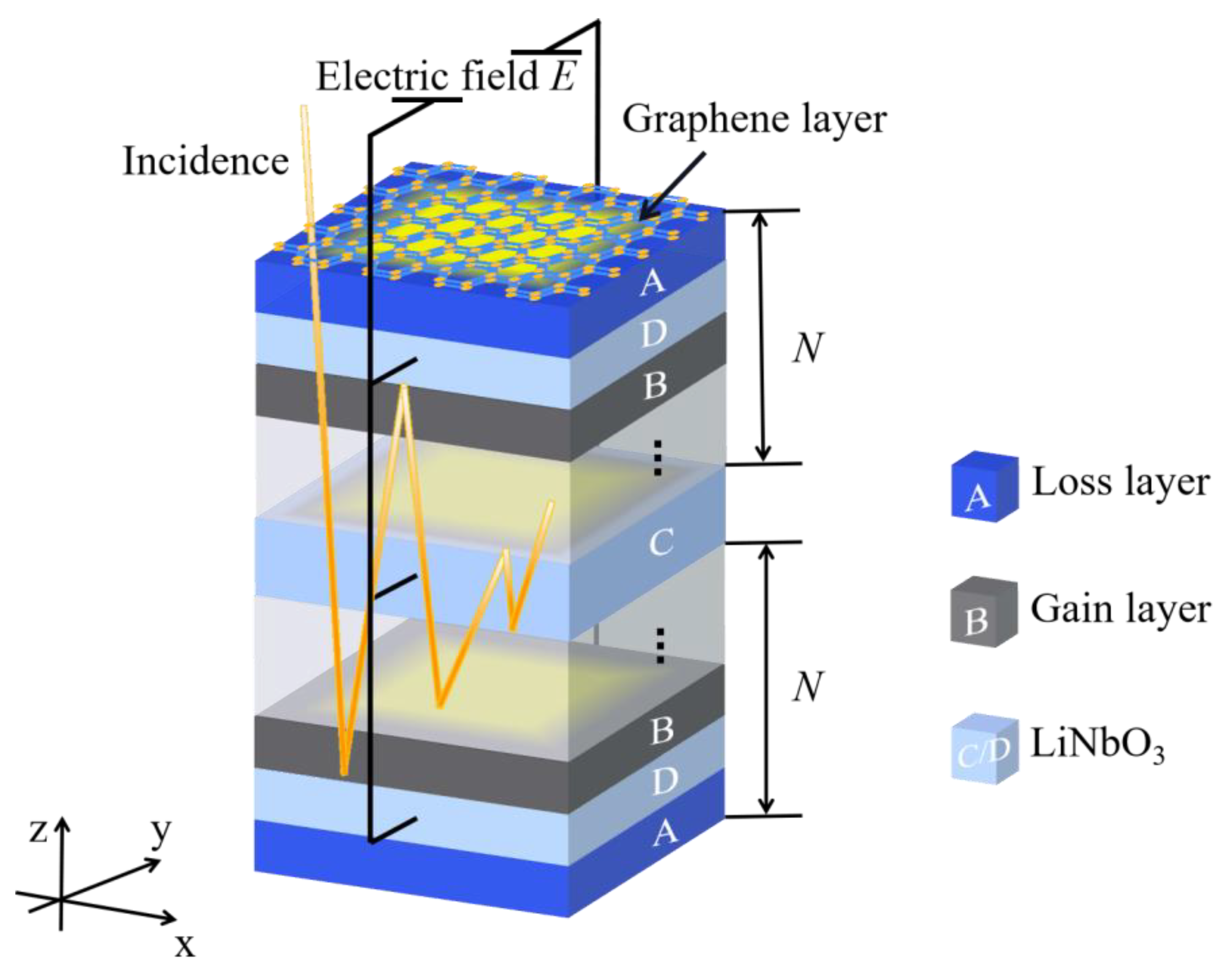
2. Model and Methods
As shown schematically in
Figure 1, the structure considered here mainly consists of a PT-symmetry PC and the top graphene layers, which can be simply represented as G
M(ADB)
NC(BDA)
N. Therein, the G deputies graphene layer is placed at the top of PT-symmetry PC;
M and
N represent the graphene layer number and PT-symmetry PC period number, respectively. For the PT-symmetry PC structure, the gain–loss layers are formed by doping quantum dots in the substrate’s dielectric silica, denoted by A and B, respectively. Such gain or loss dielectric layers can be realistically manufactured by analogy to quantum well amplifiers or photorefractive structures. We can use modified solution doping methods in the modified chemical vapor deposition (MCVD) process to develop gain-doped or loss-doped silica substrate. D and C layers represent a LiNbO
3 crystal. Different media layers can be closely stacked by microelectronics or micromechanical processes, and graphene layers can be obtained by Chemical Vapor Deposition (CVD) [
15]; the entire structure satisfies the PT-symmetry condition.
The refractive index of A or B layer can be quantitatively described by the Lorentz model [
19]:
where
γ = 2.5 × 10
14 s
−1 is damping coefficient;
ω0 = 1.216 × 10
15 s
−1 is the resonance angular frequency, which corresponds to the resonance wavelength of 1550 nm;
ω indicates the incident angle frequency; and
α is macroscopic Lorentzian oscillation intensity, which characterizes the relationship between the system’s gain, the concentration of doping quantum dots and the distribution of excited state quantum dots. When the entire structure satisfies the PT-symmetry condition, the absolute values of
α in loss layer (A) and gain layer (B) are equal. The value of α will have a great influence on the absorptance of graphene, which will be demonstrated in the 3 parts.
denotes the dielectric constant of the basal silica, which can be described by the Sellmeier dispersion relation [
20].
A LiNbO
3 crystal is a typical electro-optical medium, and its refractive index depends on the applied electric field
E; since
E is along the y-axis, the refractive index and applied electric field satisfy the ellipsoid equation. When the incident wave is TE wave, the electric field is along the y-axis. The refractive index of layer D or C can be expressed as follows [
21]:
where
n0 = 2.286;
γ = 8.6 × 10
−3 nm/V is electro-optic constant of LiNbO
3 crystal; and
E represents the applied electric field intensity along the y-axis. For practical applications, the modulated electric field is connected to the LiNbO
3 dielectric layer (D and C layer) via metal wires.
For the top graphene layer, the optical properties are closely related to its complex surface conductivity
σG. Its effective dielectric constant can be expressed as follows [
22,
23]:
where
ε0 is the vacuum dielectric constant;
dG = 0.34 nm is the thickness of monolayer graphene;
ω is the angular frequency of incident light; and
σG is the surface conductivity of graphene under random-phase approximation, which can be expressed as follows.
Herein, we have the following:
where
ℏ =
h/2π is the reduced Planck constant; e is electron charge; k
B is Boltzmann constant; T = 300 K is the Kelvin temperature;
μ is the chemical potential of graphene, which is determined by the electron concentration and can be controlled by the gate voltage U [
24]; and
τ = 0.5 × 10
−14 s denotes the relaxation time of graphene layer.
The transfer matrix method (TMM) is used to study the absorption characteristics of the structure in this paper, and the detailed description of the TMM can be obtained from the relevant literature [
19]. The absorption of the graphene layer in proposed structure can be described by the following two processes. Firstly, when incident light enters the underlying PT-symmetry PC structure through the graphene layer, the initial absorption of incident light is caused by graphene; secondly, the Bragg reflection of incident light is produced by the bottom layer PT-symmetry PC structure, when the reflected light passes through the graphene layer. We can calculate the absorption in graphene layer by using Poynting vectors [
25]:
where
and
represent the total incident and reflected Poynting vectors of the entire structure, respectively, and
and
represent the incident and reflected Poynting vectors of the PT-symmetry 1D-PC, respectively. According to the total reflection and transmission coefficient of the entire structure, the absorption of graphene can be derived by using the Poynting vector expression above:
in which r
total and r
PT represent the reflection coefficients of the total laminated structure and the underlying PT-symmetry PC structure, respectively; and t
total and t
PT represent the transmission coefficients of the overall structure and the underlying PT-symmetry PC structure, respectively.
3. Results and Discussion
In order to satisfy the PT-symmetry condition and generate the defect mode at 1550 nm, in numerical calculation, the thickness of the A and B layer is set to
dA =
dB = 524.28 nm for the underlying PT-symmetry PC; the macroscopic Lorentzian oscillation intensity in the gain–loss layer is set to
αB = −2.1 × 10
−4 and
αA = 2.1 × 10
−4. The thickness of dielectric layer D is adjusted to
dD = 455 nm, the dielectric layer C can be observed as the defect layer of the entire structure, and its thickness is set to
dC = 2
dD; without applied modulation electric field, the refractive index of D or C layer is
n0 = 2.286. The chemical potential is
μ = 0.3 ev, and the thickness is
dG = 0.34 nm for the monolayer graphene. The PT-symmetry PC structure period is
N = 6, and other structure parameters are provided in
Section 2.
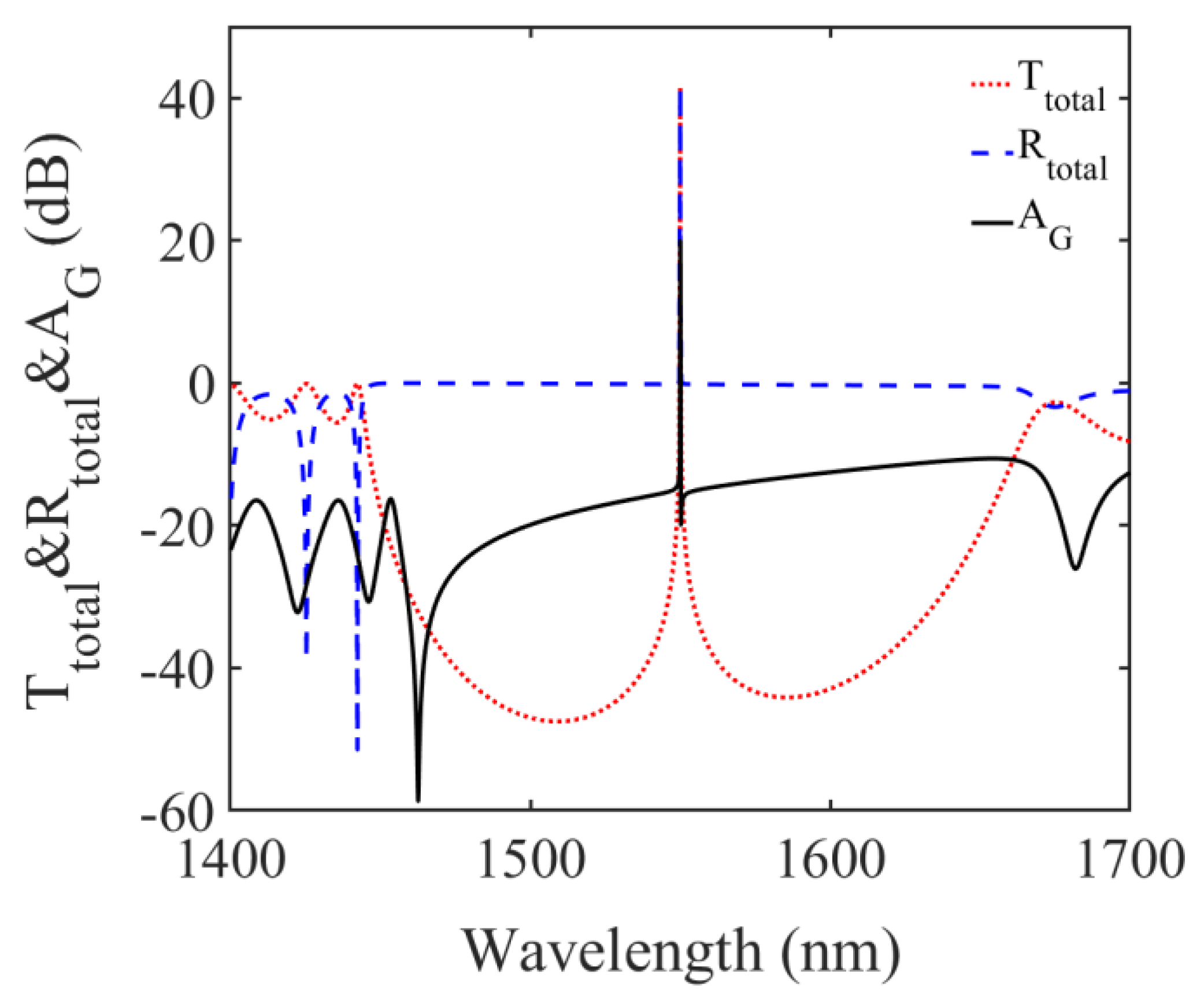
Figure 2 plots the transmission and reflection spectra of the entire structure and the absorption spectra of the monolayer graphene. In order to more intuitively present the transmission and reflection of the structure and the absorption of graphene layers at different wavelengths, here, a logarithmic transformation, with dB as the unit, is taken for the calculation, and the conversion relationship can be written as follows: Y(dB) = 10lg
Y, where
Y can represent transmission, reflection of the structure, and the absorption of graphene layers.
As clearly observed in
Figure 2, the absorption of monolayer graphene can reach 25.21 dB at a wavelength of 1550 nm, which is 14,430-fold of the absorptance of monolayer graphene in air. As observed from Equation (1), only the incident light wave with a wavelength of 1550 nm is selected; the refractive index of the A and B layer can satisfy the PT-symmetry condition strictly (the real part of the gain loss layer is even symmetric, and the imaginary part is odd symmetric), which means that under such circumstances, the PT-symmetry structure has the strongest amplification effect on the transmission and reflection of the incident light, and the graphene–light interactions are tremendously enhanced. This is the dominating cause for the ultrastrong absorption of graphene. As observed from Equation (8) and
Figure 2, both simulation results and theoretical analysis agree very well.
The macroscopic Lorentzian oscillation intensities of the PT-symmetry PC, graphene layer number and chemical potential as well as incident light angle are the predominant factors affecting graphene absorption, which will be discussed in the following section. Meanwhile, in the end, based on the optimization parameters of the structure, we also simulated the in-phase and out-phase absorption properties of graphene under the square-wave modulation electric field.
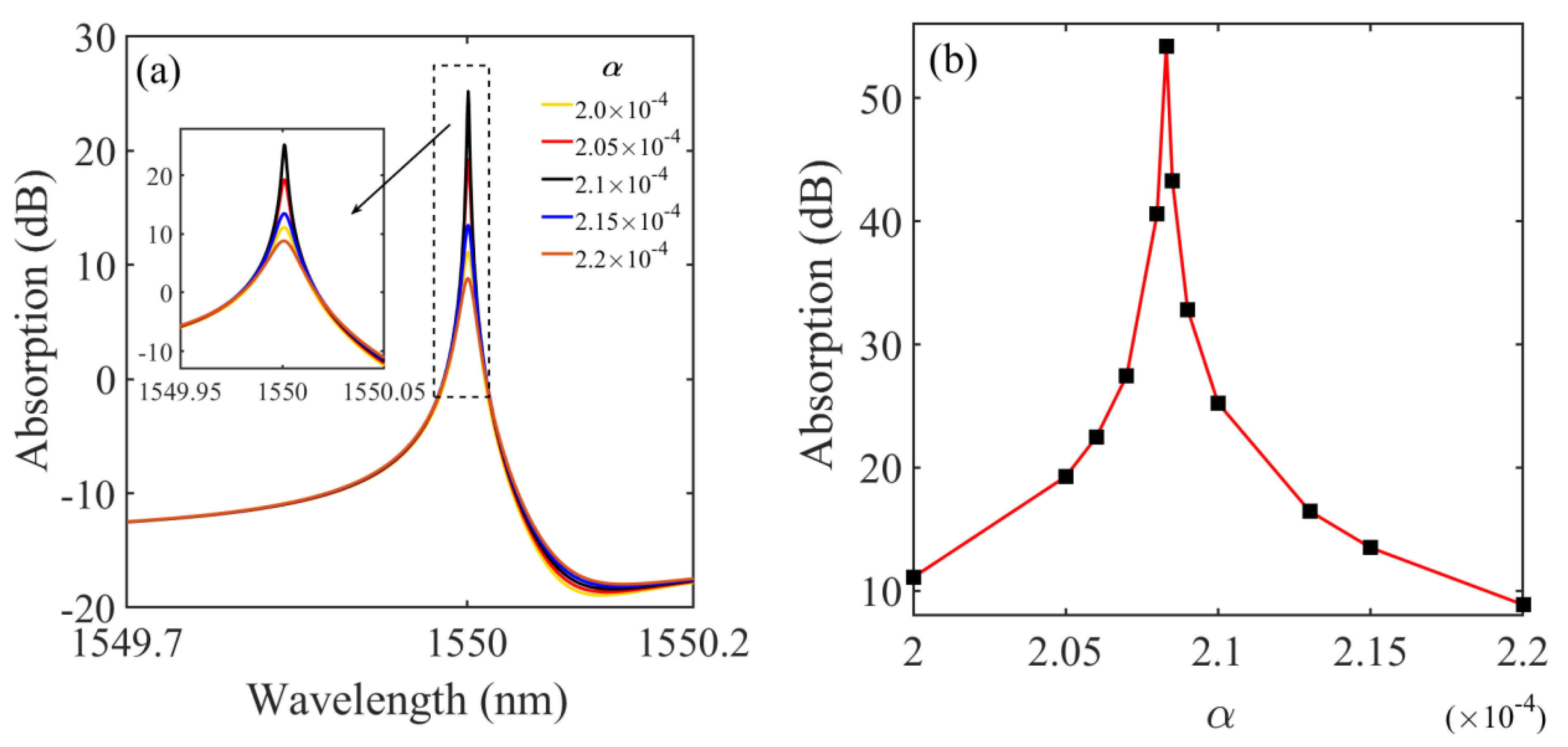
3.1. Effects of α on Absorption of Graphene
The value of the macroscopic Lorentzian oscillation intensity α has a prodigiously greater influence on the imaginary part of the gain–loss dielectric layers and then affects the resonance coupling effect of the entire structure. In order to figure out the effects of α on the absorption of graphene. First, while keeping the other parameters constant, in
Figure 3a, we present the graphene absorption spectrum with
α changing, according to the absorptance of 1550 nm light wave corresponding to different α values, we plot the changing curve of graphene absorptance with
α in
Figure 3b.
The results show that the peak position of graphene absorption, with α changing from 2 × 10
−4 to 2.2 × 10
−4, remains unchanged while the absorptance of graphene changed remarkably, which manifest a tendency to increase first and then decrease with the results shown in
Figure 3b. The absorptance of monolayer graphene is as high as 54.22 dB when α = 2.0385 × 10
−4, which is seven orders of magnitude higher than the absorption of monolayer graphene. This is because the resonant coupling effect of the structure is the strongest at the wavelength of 1550 nm when α = 2.0385 × 10
−4, and the bottom PT-symmetry PC has the highest efficiency in converting pump energy into incident light wave electromagnetic energy, which makes the transmission and reflection of the structure much higher than one, thus enhancing the absorptance of the top graphene layer.
It is worth noting that even a small fluctuation near the peak value of α will have a large effect on the absorption of graphene. For practical applications, it is a challenge to control α precisely in this order of magnitude. Without losing generality and selecting α = 2.1 × 10⁻⁴ in the calculation, the absorption of graphene can reach 25.21 dB at this α value, which can sufficiently meet the performance of graphene-based photoelectric detection devices. Meanwhile, considering device performance and working stability, we are more inclined to improve the absorptance by reasonably setting the number and chemical potential of graphene layers in the actual design. The effects of different chemical potentials and graphene layers on absorption efficiency are discussed below.
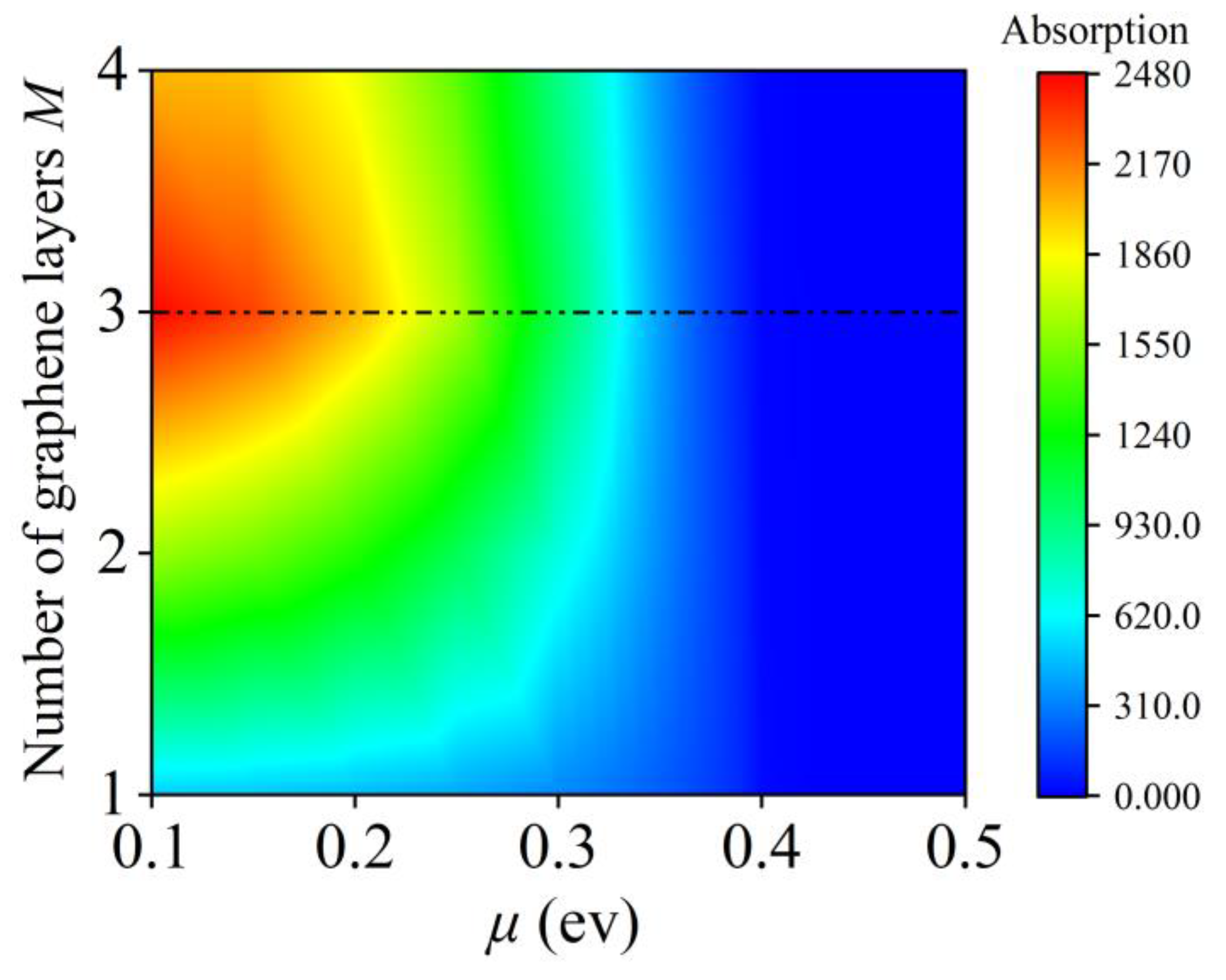
3.2. Effects of M and μ on Absorption of Graphene
The thickness of monolayer graphene is only 0.34 nm. Therefore, increasing the number of graphene layers has little effect on the position of the absorption peak, the simulation results show that for each additional layer of graphene, the absorption peak only produces a blueshift of 0.001 nm, while the number of layers has a great influence on the absorptance of graphene. In order to obtain the entire change tendency of graphene absorption with the number of layers and chemical potentials, by increasing the number of graphene layers, we calculate the total absorption of graphene layers corresponding to different chemical potentials. The 2D view of absorptance is shown in
Figure 4.
It can be observed from
Figure 4 that for a constant graphene chemical potential value, the absorptance reaches the maximum when the number of graphene layers reaches three. Meanwhile, the absorptance of different layers decreases gradually with an increase in chemical potential. Graphene absorption precipitately drops to nearly zero when the chemical potential approaches 0.4 ev. When the chemical potential is greater than 0.4 ev, the graphene layer absorptance tends to zero and does not change any longer.
Table 1 shows the absorptance of graphene at different chemical potentials when the number of graphene layers taken is three.
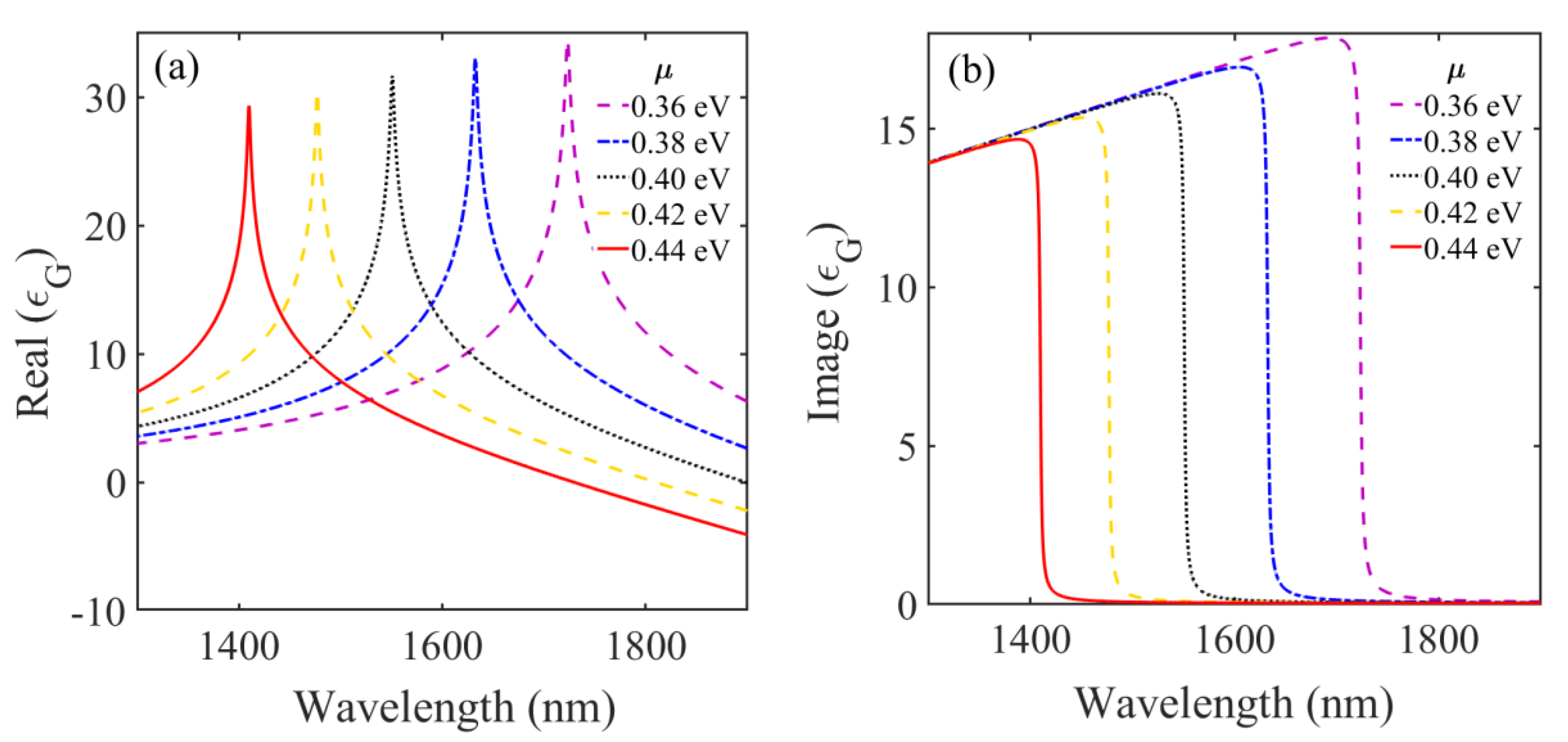
In order to account for this phenomenon more intuitively, in
Figure 5, we plotted the variation curves of the real and imaginary parts of the graphene dielectric constant with the wavelength (the chemical potential changing from 0.36 ev to 0.44 ev in steps of 0.02 ev). For different chemical potentials, the spike in the real part of the graphene dielectric constant corresponds to the sudden fall of the imaginary part, which is shown in
Figure 5a,b. Furthermore, as the chemical potential decreases, the features (the spike and the sudden fall dot) of the real and imaginary parts of the graphene permittivity have a quick redshift in the investigated wavelength range from 1300 nm to 1800 nm. Simulation results show that when
μ = 0.42 ev, the feature of the real and imaginary parts corresponds to the wavelength of 1550 nm, which is the dominating reason for rapid decrease in graphene absorption at 1550 nm.
The chemical potential of graphene can be effectively tuned by the gate voltage U; hence, electrical switching of graphene absorption at 1550 nm can be achieved by the gate voltage. Finally, it should be mentioned that the chemical potential is related to the thickness and dielectric constant of the isolation medium filled between graphene. Considering practical application, the chemical potential is taken as μ = 0.3 ev in the following calculation.
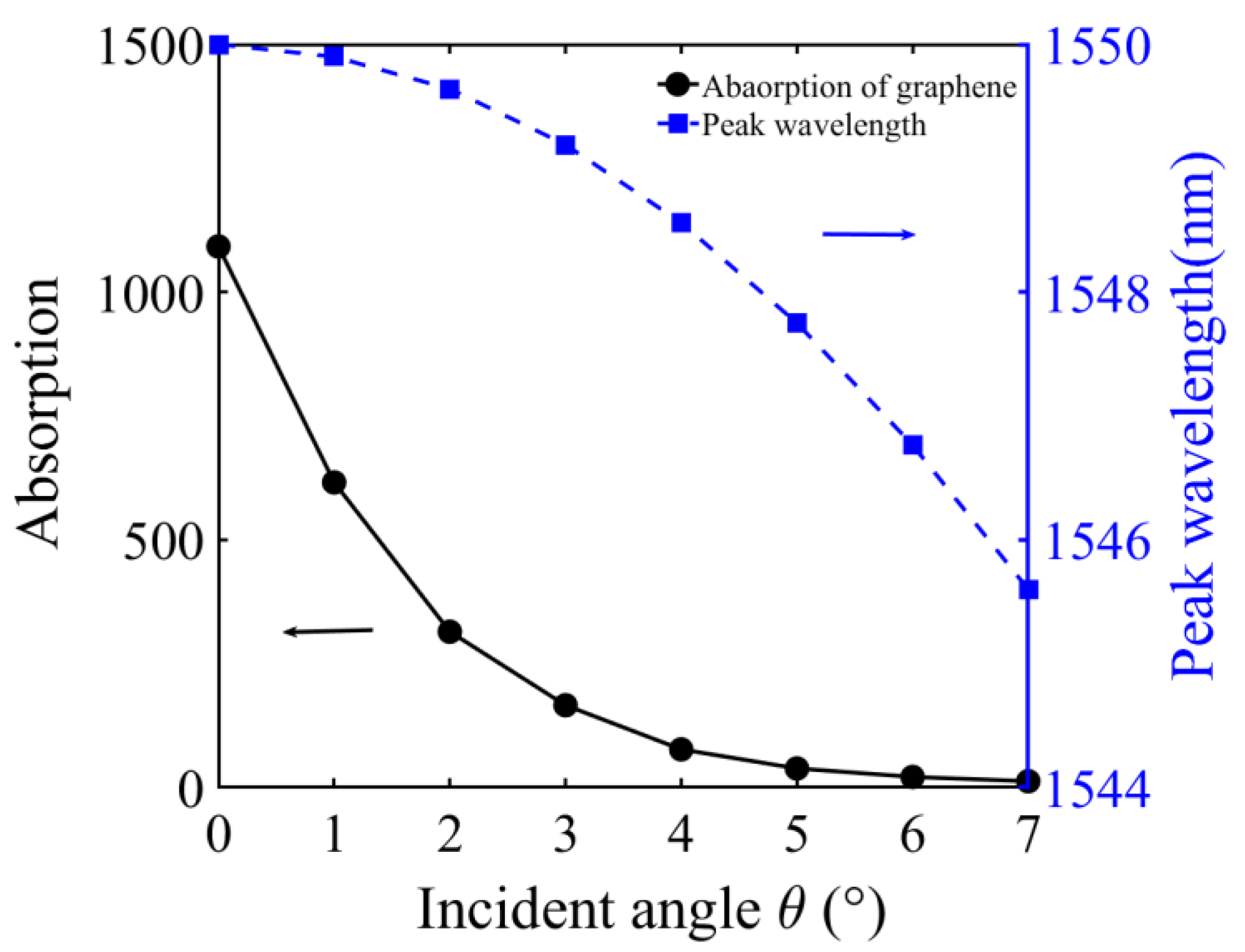
3.3. Effects of θ on Absorption of Graphene
The incident angle is a momentous factor affecting the absorptance of graphene. When the incident angle
θ changes, the position of the defect mode will deviate from the strong coupling point of the PT-symmetry structure, and then the coupling effect of the bottom PT-symmetry PC will also change, which is the reason for the changes in the graphene absorption patterns (the position and absorptance). Based on the high sensibility of graphene absorption on incident angle
θ, 1° is the angle interval set in the calculation. The chemical potential
μ and the number of graphene layers
M in our numerical simulation are be fixed at 0.3 ev and 3, respectively. The influences of the incident angle on the absorptance and absorption peak position of the structure G
M(ACB)
ND(BCA)
N are investigated and plotted in
Figure 6, respectively.
As observed from
Figure 6, when the incident angle deviates 0°, the absorption mode, deviating from on-resonance position, experiences blueshift, and absorption simultaneously dropped from 1092 (30.4 dB) to 12.7 (11.0 dB) quickly, while the incident angle changes by only 7°. Tracing the position of the absorptance with respect to the reactive energy perturbation has been a common sensing mechanism, and this angle dependence points to the fact that the structure can be designed as a direction sensor. Due to such angular susceptibility, care has to be taken to ensure that the absorptance of graphene is maximum. The electro-optic modulation characteristics of LiNbO
3 crystal for graphene absorption are discussed below, and the vertical incident TE wave is still selected to be carried out.
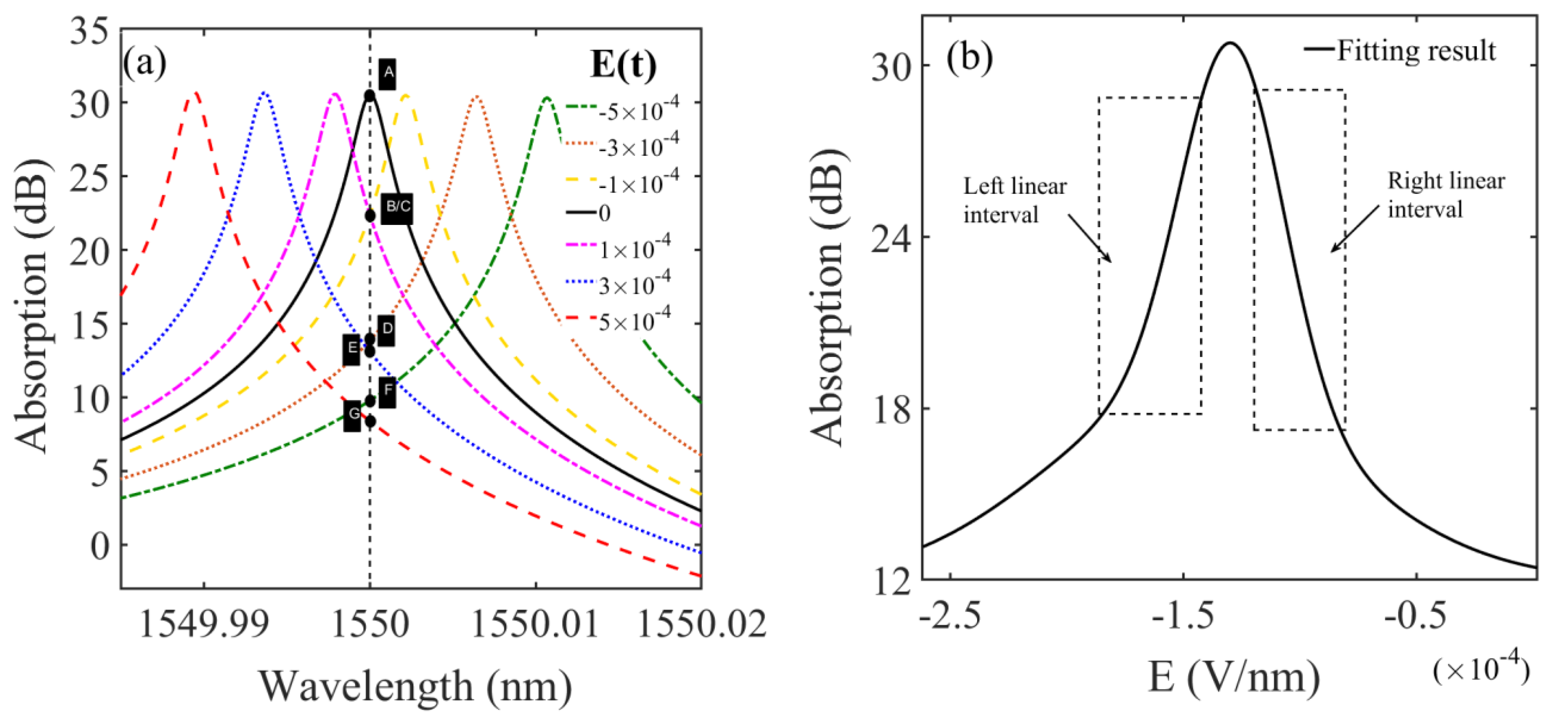
4. Modulation of Absorption by Applied Electric Field E
It can be straightforwardly observed from Equation (3) that the refractive index of the LiNbO
3 crystal is related to the applied electric field. Accordingly, the electro-optic modulation based on LiNbO
3 is primarily realized by adjusting the intensity of applied electric field. First, the variation range of electric field along the
y-axis is selected from −5 × 10
−4 to 5 × 10
−4 V/nm. At different modulation electric field values, the absorption spectra of graphene are plotted, as shown in
Figure 7a. Then, we plotted the best fit of the graphene absorption at 1550 nm (from A to G in
Figure 7a) based on the second-order Gaussian fitting, which is shown in
Figure 7b.
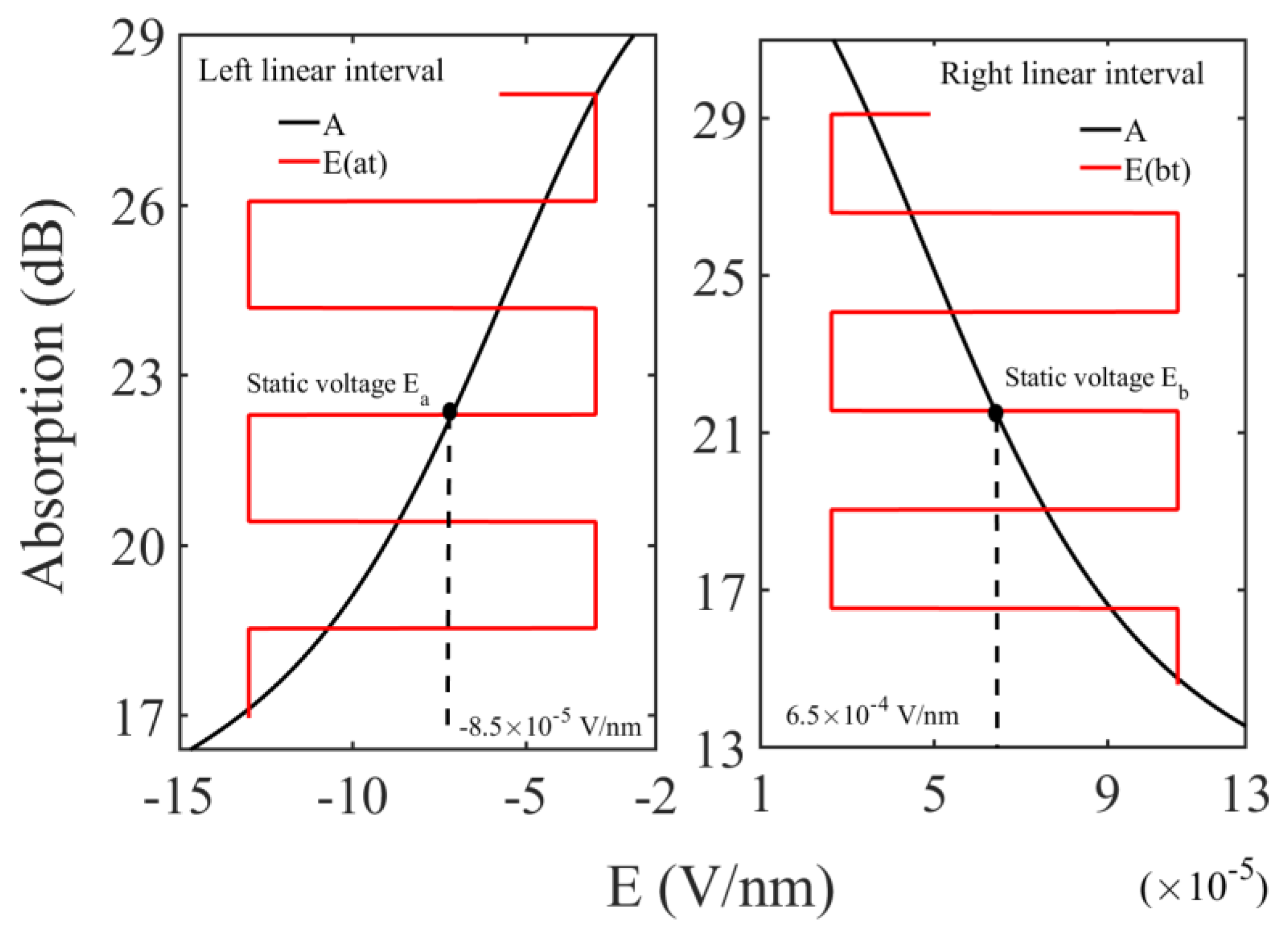
We can, through the study, obtain that of the two linear intervals near the peak value in
Figure 7b, the absorption of graphene exhibits an identical trend with the increase in modulation electric field
E(t) in opposite directions. Based on the electro-optic modulation of LiNbO
3, reversible modulation of graphene absorption can be achieved. First, a static bias electric field (
Ea or
Eb shown in
Figure 8) was elaborately selected in two linear intervals. On that basis, the square-wave modulation electric field signal is the input, and the value of the square-wave electric field can be set according to the range of the linear interval. Accordingly, in two linear intervals, the bias electric field acting on LiNbO
3 can be expressed as
Ea+
E(at) and
Eb+
E(bt).
As shown in
Figure 8, the absorptance of graphene will show in-phase and out-phase modulation with the square wave electric field changes. For the negative electric field, the static bias electric field
Ea = −8.5 × 10
−5 V/nm,
E(at), is the square-wave electric field with an electrical level of 5 × 10
−5 V/nm. The in-phase absorption from 17 dB to 28 dB occurred with
E(at) changing from −5 × 10
−5 V/nm to 5 × 10
−5 V/nm. For the positive electric field, the static bias electric field
Ea = 6.5 × 10
−5 V/nm,
E(bt), is the square-wave electric field with an electrical level of 4.5 × 10
−5 V/nm, and likewise, the out-phase absorption from 30 dB to 15 dB occurred with
E(bt) changing from −4.5 × 10
−5 V/nm to 4.5 × 10
−5 V/nm. The electric field modulation parameters and graphene absorption values are listed in
Table 2.
5. Conclusions
A novel PT-symmetry 1D-PC microcavity structure GM(ADB)NC(BDA)N was proposed. Therein, the underlying PT-symmetry structure is mainly composed of the gain-loss dielectric layers and the embedded LiNbO3 crystal, and the graphene layers are placed on the top of the PT-symmetry structure. According to the precise matching of gain–loss dielectric layers and the strong coupling effects caused by PT-symmetry PC under graphene layer, the absorptance of graphene can be enhanced predominantly. Additionally, by utilizing the electric-optical effect of LiNbO3 crystal, an electrically modulated absorption of graphene based on the structure has been realized. The influences of macroscopic Lorentzian oscillation intensity α, graphene layers M and chemical potential μ, incident light angle θ, and modulation electric field on the absorption of graphene were numerically investigated by the TMM in this paper. The results show that when Macroscopic Lorentzian oscillation intensity is equal to 2.1 × 10⁻⁴, the layer number and chemical potential of graphene are equal to 3 and 0.3 ev, respectively; the absorptance of graphene to 1550 nm optical wave is close to 30.4 dB. Meanwhile, the in-phase and out-phase absorption of graphene with a modulation electric field can be realized by reasonably setting the electric field parameters. The reported results describe the application potential of the proposed graphene-based optical structure.


