Abstract
The resistive memory has become one of the most promising new memory types because of its excellent performance, and HfO2 resistive material has attracted extensive attention. The conduction mechanism based on oxygen vacancy is widely recognized in the research of new nonvolatile memory. An RRAM electrothermal coupling model based on the oxygen vacancy conduction mechanism was constructed using COMSOL. The resistance process of the device is simulated by solving the coefficient partial differential equation, and the distribution of oxygen vacancy concentration, temperature, electric field, electric potential and other parameters in the dielectric layer at different voltages are obtained. The effects of temperature, dielectric layer thickness, top electrode thermal conductivity and conductive wire size on the resistance characteristics of the device are studied. It has guiding significance to further study the RRAM mechanism.
1. Introduction
With the development of science and technology, the demand for high-performance computers is increasing day by day. With the improvement of the integration and performance of semiconductor chips, mainstream memory has reached the bottleneck of development. Faced with severe challenges, there is an urgent need to find a new type of memory with high speed, high durability and low power consumption to replace flash memory. Resistive memory has become the most potential new type of non-volatile memory because of its tiny size, fast storage speed, high durability, non-volatile characteristics and good compatibility with CMOS technology [1,2]. The resistance conversion mechanism varies with the materials that make up RRAM devices. The resistive memory based on binary metal oxides has the most potential for development because of its excellent performance. Among them, HfO2 thin film as a high K dielectric material has the advantages of a high dielectric constant and wide band gap [3,4].
Based on the experimental results, the researchers established the current model to explain the resistance variability of the RRAM [5,6,7]. For example, Jiang Z. et al. [7] proposed a model suitable for multilayer RRAM and can systematically calibrate the model parameters by experiment. However, this kind of model is used more in large-scale circuit simulation [5]. In many studies on the resistance mechanism based on oxide RRAM, the oxygen vacancy conductive filament mechanism is widely recognized [8,9,10,11,12]. The mechanism is that the migration of oxygen vacancies under the action of an electric field leads to the formation or fracture of conductive filaments, resulting in the transformation of high and low resistance states of the device [13,14]. Therefore, in order to simulate the physical mechanism of RRAM, the comprehensive effect of electric field and Joule heat on the resistance variation characteristics of the device should be considered at the same time. Chang F. et al. [15,16,17,18] studied the physical mechanism of unipolar resistance switching based on SiOx-RRAM through experiment and simulation. Kim S. et al. [19] proposed an electro-thermal resistance switching model based on tantalum-oxide-based RRAM by finite element method. González G. et al. [20] completed the physical modeling considering device capacitance and parasitic resistance based on TiN/Ti/HfO2/W stack. The model also considers the thermal description of the dielectric layer outside the conductive filament.
In this paper, an electro-thermal coupling model of HfOx-based RRAM is established by COMSOL. The previous RRAM simulation only considered the effect of oxygen vacancy on the resistive characteristics, but the oxygen vacancy recombination also played an important role in the resistive mechanism of the device. Therefore, a more accurate RRAM model is established based on the single-layer structure of Pt/HfO2/Ti in this work.
2. Models
The simulation of the device focuses on the establishment of physical field and model. COMSOL multi-physical field numerical simulation software includes simulation models of electromagnetic, heat transfer, structural mechanics and other physical fields, which can be used for coupling, calculation and analysis of multi-physical fields. This paper uses the finite element analysis method to simulate the device model, which involves three physical models: ion migration model, electrical conduction model and Joule heat model.
In the previous work, the switching characteristics of a series of Pt/HfOx/Ti RRAM were studied [21,22,23]. On the basis of previous experimental research, in this paper, the Pt/HfO2/Ti model is simulated. The model is a typical MIM structure and the resistive dielectric layer is HfO2. As shown in Figure 1, the model is created using 2D axisymmetric components. In order to simplify the analysis, assuming that only one conductive filament is generated, CF is defined as the region in the dielectric layer where the conductive filament is generated, with a radius of 5 nm and a height of 10 nm. In order to simulate the on-off of conductive wire, the conductive part in the HfO2 dielectric layer is divided into two parts. The lower part is the embryonic part of conductive wire, with high oxygen vacancy concentration, which can be defined as HfOx. The upper part is the broken part of conductive wire, with low oxygen vacancy concentration. Table 1 shows the material properties used in this simulation.
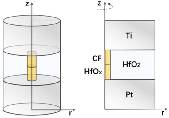
Figure 1.
Pt/HfO2/Ti RRAM structure model, the side length does not represent the true proportion.

Table 1.
Material properties of each part of the model.
The properties of CF need to be customized. Firstly, it is assumed that the density and heat capacity are equal to HfO2. The electrical conductivity σ and thermal conductivity kth of CF are related to the change of oxygen vacancy concentration. The pre-exponential factor σ0 and the conductance activation energy Eac in the conductivity σ are functions of oxygen vacancy concentration. The functional relationship between the pre-exponential factor of electrical conductivity σ0, thermal conductivity kth, conductivity activation energy Eac and oxygen vacancy concentration is shown in Figure 2.
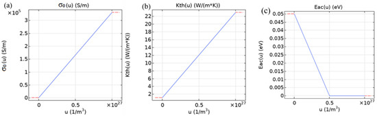
Figure 2.
The functional relationship between oxygen vacancy concentration nude and (a) the pre-exponential factor σ0, (b) thermal conductivity kth, (c) conductivity activation energy Eac.
The initial conditions of the voltage are as follows: the upper electrode is connected to the voltage, and the lower electrode is always grounded. In the process of simulation, the parameterized scanning voltage can be applied to the upper electrode to obtain the changes of oxygen vacancy concentration, temperature, electric potential and electric field. The upper and lower electrodes and boundaries of the device are at room temperature. The oxygen vacancy concentration of the conductive filament is the maximum doping concentration, and the initial oxygen vacancy concentration of the non-conductive filament is 0.
3. Results and Discussion
3.1. Simulation of Reset Process
In the Reset process simulation, it is assumed that the conductive filament is in a fully conducting state at the beginning, and the top electrode applies a negative scanning voltage (−0.6 V, −0.7 V, −0.8 V, −0.9 V) respectively.
From the distribution diagram of oxygen vacancy concentration in Figure 3, it can be seen that when the voltage is −0.6 V, the oxygen vacancy concentration in the dielectric layer is uniformly distributed and the conductive filament is conductive. With the increase in the voltage, the oxygen vacancy at the junction of the upper and lower region begins to move to the top electrode. At this time, the device has not yet carried out the resistance conversion, and the conductive filament is still in the conduction state. When the voltage reaches −0.7 V, the oxygen vacancy concentration at the junction of the upper and lower regions decreases to 0.8 × 1027 m−3, and the conductive filament is still in the conduction state. When the negative voltage increases to −0.8 V, the oxygen vacancy concentration at the junction reaches 0.5 × 1027 m−3 and the conductive filament begins to break. When the voltage reaches −0.9 V, the conductive filament breaks obviously, and the oxygen vacancy concentration at the junction is as low as 0.1 × 1027 m−3. The device completes the Reset process and changes from a low resistance state to a high resistance state. At this time, the oxygen vacancy is mainly accumulated near the top electrode.
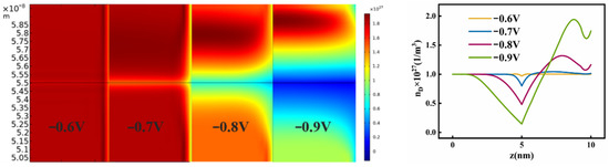
Figure 3.
Two-dimensional and one-dimensional diagrams of oxygen vacancy concentration distribution under different bias voltages.
Figure 4 shows the temperature distribution in the dielectric layer during the Reset process. It can be seen that in the initial state, the temperature distribution is regularly symmetrical, and the temperature at the junction of the upper and lower regions is the highest. With the increase in the reverse bias voltage, the temperature gradually rises. When the voltage is −0.9 V, the position of the highest point remains unchanged, but the curve is distorted, and the highest point of temperature becomes more prominent and no longer smooth. This is because the conductive filament was broken at this time, the device is in a high resistance state, and the current in the dielectric layer decreases rapidly, so the joule heat generated will be lower than that in the conduction state. At the same time, it is found that the temperature changes fastest at the junction of the upper and lower half of the region with the increase in voltage. It is because that the temperature is the highest, the migration rate of oxygen vacancy is the fastest, and the conductive filament will break in the place with the highest temperature.
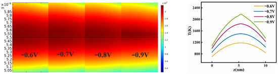
Figure 4.
Two-dimensional and one-dimensional diagrams of temperature distribution under different bias voltages.
Figure 5 shows the distribution of the electric field in the dielectric layer under different bias voltages. The results show that there is a “Winner-take-all” phenomenon in the dielectric layer, that is, under the action of applied voltage, the electric field will produce non-uniform distribution with the non-uniform distribution of oxygen vacancy concentration [24]. It can be seen that because of the large resistance at the fracture, the partial pressure increases greatly, so the electric field gradually shifts to the fracture of the conductive filament. When the voltage is −0.6 V, the oxygen vacancy concentration in the dielectric layer is equal everywhere, so the electric field is uniformly distributed. With the gradual increase in the voltage, the peak of the electric field gradually approaches the center of the upper and lower region. When the voltage is −0.8 V, the electric field intensity in the center of the dielectric layer is extremely high, while the electric field intensity in other regions is nearly zero. It shows that the device completes the Reset process and the conductive filament is completely broken.
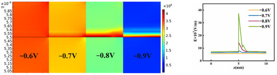
Figure 5.
Two-dimensional and one-dimensional diagrams of electric field distribution under different bias voltages.
3.2. Simulation of Set Process
The forward voltage is applied to the device to simulate the Set process. Figure 6 shows the distribution of oxygen vacancy concentration in the dielectric layer during the set process. As can be seen from the figure, when the voltage is 0.8 V, the lowest oxygen vacancy concentration in the film is close to zero, indicating that the conductive filament is still in the fracture state and the device is in the high resistance state. With the increase in voltage, the oxygen vacancy concentration at the fracture of the conductive filament increases gradually, and the oxygen vacancy concentration near the upper electrode begins to decrease. When the voltage is 0.88 V, the conductive filament is turned on again. When the voltage is 0.92 V, the conductive filament breaks again, and the fracture area is close to the top electrode.
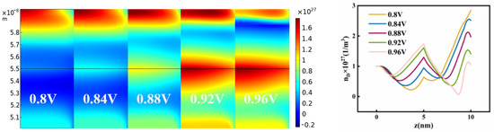
Figure 6.
Two-dimensional and one-dimensional diagrams of oxygen vacancy concentration distribution under different bias voltages.
Figure 7 shows the temperature distribution in the dielectric layer under different bias voltages. It can be seen that when the voltage is 0.8 V, the conductive filament is still in the state of fracture, and the highest temperature is located at the fracture. With the increase in voltage, the transfer rate of oxygen vacancy increases and the temperature of conductive filament becomes higher. When the voltage is between 0.88 V and 0.92 V, the temperature in the lower half of the film is basically unchanged, indicating that the conductive filament is reconnected and the resistance no longer changes. The internal temperature of the filament no longer changes with the increase in voltage. Continue to increase voltage, the highest point of temperature moves towards the area close to the upper electrode. When the voltage is 0.96 V, the conductive filament breaks at the highest temperature near the top electrode, which is mainly because the oxygen vacancy migration is carried out under the combined action of the electric field and temperature. However, the peak temperature will be lower than that when conducting, because the fracture position is in a state of high resistance, the current decreases rapidly, and the Joule heat will be reduced accordingly.
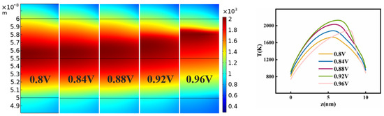
Figure 7.
Two-dimensional and one-dimensional diagrams of temperature distribution under different bias voltages.
Figure 8 shows the distribution of electric field modes in the dielectric layer during the Set process. It can be seen that when the voltage is 0.8 V, the conductive filament is still in a state of fracture. The electric field strength at the fracture is very strong, and the oxygen vacancy gradually escapes under the action of the electric field. With the increase in voltage, the electric field increases gradually, and the peak value moves near the top electrode. When the voltage reaches 0.88 V, the one-dimensional diagram of the electric field begins to connect, indicating that the conductive filament is reconnected. When the voltage reaches 0.96 V, the electric field intensity near the top electrode is extremely high, and the electric field intensity in other areas is very small, and the conductive filament breaks again.
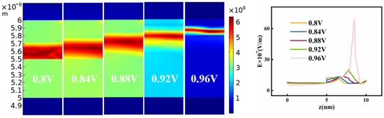
Figure 8.
Two-dimensional and one-dimensional diagrams of electric field distribution under different bias voltages.
The experimental data are also combined to test whether the model can accurately reflect the internal mechanism of the device. Figure 9 shows the I-V characteristic curves of the RRAM obtained by simulation and experiment. It can be seen that the curve of the reset process of the experiment and simulation is consistent, the change of resistance is slow, and the reset voltage is basically the same. Because of the initial resistance setting in the simulation, the current in the set process is larger than the experimental result, but the trend of the curve is basically the same, the change of resistance is all abrupt. Because the limited current is used to protect the device from a breakdown in the experiment, the current change after being set in the simulation is different from the experimental results. The simulation results are in good agreement with the experimental results. This model can be used to analyze the internal mechanism of RRAM.
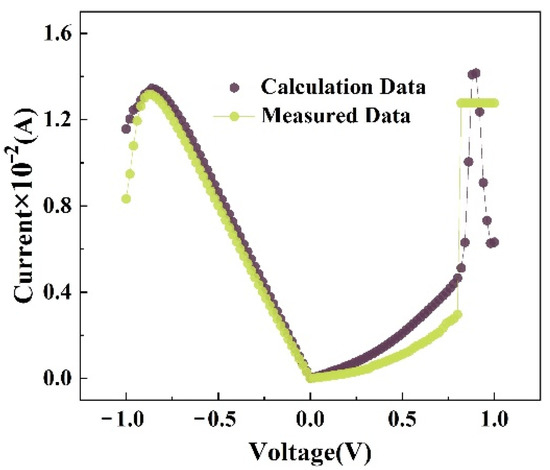
Figure 9.
Comparison between simulation and experimental results of I-V characteristic curve.
3.3. The Influence of Parameters on the Resistance Characteristics
The fracture of conductive filament is the result of ion migration, and the temperature has a great influence on the migration and diffusion rate. Here, the resistance variation process of the device at different temperatures is simulated by setting different boundary temperatures (293 K, 343 K, 393 K, 443 K). Figure 10a shows the Reset I-V characteristic curve at different temperatures. It can be seen that the change of on-state current at different temperatures is not obvious. With the increase in temperature, the reset voltage gradually decreases. This is because the generation probability of oxygen vacancy is directly proportional to the temperature. With the increase in temperature, the mobility of oxygen vacancy will also increase, so the reset voltage will decrease. This is consistent with the experimental results obtained by Chao Lu et al. [25], which further proves that the established electro-thermal coupling model is accurate. The thermal energy of oxygen vacancies and ions increases, and such a strong electric field is not required to establish or destroy conductive filaments [26]. Figure 10b shows the change of oxygen vacancy concentration near the fracture of conductive filament at different temperatures. It can be seen that with the increase in temperature, the oxygen vacancy concentration decreases more, and the reset voltage required to reach the breaking concentration will also decrease. In conclusion, the temperature has a certain effect on the fracture of conductive filaments.
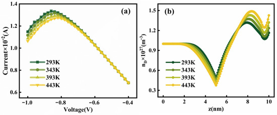
Figure 10.
(a) Reset I-V characteristic curve of the device at different temperatures. (b) oxygen vacancy concentration at the fracture of conduction band filament.
The dielectric layer thickness will also affect the resistance transition of the device. The reset process when the dielectric layer thickness is set to 8 nm, 10 nm and 12 nm respectively is also studied. It can be seen from Figure 11 that with the increase in the thickness of the dielectric layer, the reset voltage of the device increases and the current during resistance value transition decreases. This is because the thicker the dielectric layer is, the greater the voltage required between the upper and lower electrodes in the resistance transformation process of the device. It has obtained the same conclusion in our previous experimental research [22], and what is more, it is also applicable to unipolar SiOx-based RRAM which are also conductive filaments mechanisms [15,16].
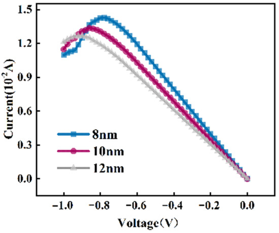
Figure 11.
I-V curves of reset process with different dielectric layer thickness.
This simulation is an electrothermal coupling model, which needs to consider not only electrical parameters such as relative permittivity and conductivity but also thermal properties such as thermal conductivity and heat capacity. The resistance characteristic of the device is simulated by changing the thermal conductivity of the top electrode. In the previous study, the thermal conductivity of the top electrode Ti is 21.9 W/(m·K). Here, the thermal conductivity of the top electrode is set to 11.9 and 31.9, respectively, and the characteristic curve and temperature change of the device under different conductivities are obtained, as shown in Figure 12.
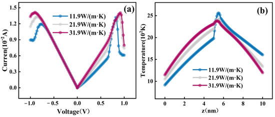
Figure 12.
Effect of thermal conductivity of top electrode on (a) I-V characteristic curve and (b) temperature.
As can be seen from Figure 12a, with the increase in the thermal conductivity of the top electrode, the voltage and current of both the Reset and Set will increase. Because of the increases in thermal conductivity, the heat loss of the Joule heat generated by the device through the electrode during the resistance conversion process will increase. It results in less heat accumulated in the dielectric layer at the same current density, lower temperature and lowers the oxygen vacancy transfer rate, so the Reset voltage will increase. As for the Set process, the off-state current increases with the increase in the thermal conductivity of the top electrode. The higher the thermal conductivity, the more difficult the device is to Reset, so the high resistance is smaller. Figure 12b shows the temperature distribution in the dielectric layer when the voltage is -1 V. It can be seen that in the broken part of the conductive filament, the lower the thermal conductivity is, the more distorted the temperature curve is. It indicates that the greater the fracture degree of the conductive filament is, the fracture is more likely to occur under the same voltage. Wei W. et al. [27] proved that a HfOx-based RRAM with a faster switching speed was obtained by adding a low thermal conductivity dielectric layer.
In order to study the effect of the top electrode thermal conductivity on the fracture position of the conductive filament of the device. On the basis of Reset, the positive scanning voltage from 0 V to −1 V was applied to the devices with thermal conductivity of 11.9 W/(m·K) and 21.9 W/(m·K), respectively. It was found that the conductive filament broke again at 1 V. Figure 13 shows the temperature distribution in the dielectric layer during fracture. It can be seen that with the increase in the thermal conductivity of the top electrode, the fracture of the conductive filament moves further away from the top electrode and moves into the dielectric layer. This is because the greater the thermal conductivity of the top electrode, the easier the heat near the electrode is lost through the electrode, resulting in the temperature peak gradually close to the inside of the dielectric layer. The higher the temperature is, the faster the oxygen vacancy transfer rate is. The conductive filament fracture often occurs in the place with the highest temperature, so the filament fracture position is closer to the inside of the dielectric layer, which is consistent with the previous research conclusion.
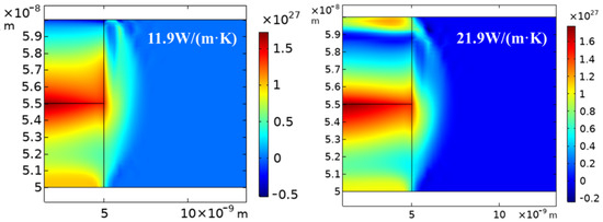
Figure 13.
Effect of thermal conductivity of top electrode on fracture position of conductive filament.
4. Conclusions
Based on the oxygen vacancy conduction mechanism, the electro-thermal coupling model of RRAM is established by using COMSOL. The resistive characteristics of the device are simulated. The electro-thermal coupling model of single-layer RRAM is established by using a 2D axisymmetric structure. By solving the oxygen vacancy transfer equation, conductance continuity equation and heat conduction equation, the Reset and Set processes of the device under different bias voltages are simulated, and the oxygen vacancy concentration, temperature, electric potential and electric field of the device are analyzed. Finally, combined with the actual test of the I-V characteristic curve, the established model is verified. The influence of the thermal conductivity of the top electrode on the resistive characteristics of the device is studied, and the cause is analyzed. At the same time, by comparing the actual test results, the accuracy of the model is further verified.
Author Contributions
Conceptualization, J.L. and S.Z.; methodology, S.W.; software, S.Z. and J.L.; validation, J.L., S.Z. and S.W.; formal analysis, S.Z.; investigation, J.L.; resources, H.L.; data curation, J.L.; writing—original draft preparation, J.L. and S.Z.; writing—review and editing, J.L.; visualization, S.W.; supervision, H.L.; project administration, S.W.; funding acquisition, H.L. All authors have read and agreed to the published version of the manuscript.
Funding
This research was funded by the Science and Technology Project of Headquarters of State Grid Corporation of China (5700-201941314A-0-0-00).
Institutional Review Board Statement
Not applicable.
Informed Consent Statement
Not applicable.
Data Availability Statement
Data is contained within the article.
Conflicts of Interest
The authors declare no conflict of interest.
References
- Kahng, D.; Sze, S.M. A floating gate and its application to memory devices. Bell Labs Tech. J. 2013, 46, 1288–1295. [Google Scholar] [CrossRef]
- Yu, S.; Lee, B.; Wong, H. Metal oxide resistive switching memory. Funct. Met. Oxide Nanostruct. 2012, 149, 303–335. [Google Scholar]
- Petzold, S.; Miranda, E.; Sharath, S.U.; Munoz-Gorriz, J.; Vogel, T.; Piros, E.; Kaiser, N.; Eilhardt, R.; Zintler, A.; Molina-Luna, L.; et al. Analysis and Simulation of the Multiple Resistive Switching Modes Occurring in HfOx-based Resistive Random Access Memories Using Memdiodes. J. Appl. Phys. 2019, 125, 234503. [Google Scholar] [CrossRef] [Green Version]
- Vandelli, L.; Padovani, A.; Larcher, L.; Broglia, G.; Pavan, P. Comprehensive physical modeling of forming and switching operations in HfO2 RRAM devices. In Proceedings of the 2011 International Electron Devices Meeting, Washington, DC, USA, 5–7 December 2011; Volume 17, pp. 1–4. [Google Scholar]
- Gonzalez-Cordero, G.; Gonzalez, M.; Garcia, H.; Campabadal, F.; Dueñas, S.; Castán, H.; Jiménez-Molinos, F.; Roldan, J. A Physically Based Model for Resistive Memories Including a Detailed Temperature and Variability Description. Microelectron. Eng. 2017, 178, 26–29. [Google Scholar] [CrossRef]
- Ambrogio, S.; Milo, V.; Wang, Z.; Balatti, S.; Ielmini, D. Analytical Modeling of Current Overshoot in Oxide-based Resistive Switching Memory rram. IEEE Electron Device Lett. 2016, 37, 1268–1271. [Google Scholar] [CrossRef]
- Jiang, Z.; Wu, Y.; Yu, S.; Yang, L.; Song, K.; Karim, Z.; Wong, H.S.P. A Compact Model for Metal–oxide Resistive Random Access Memory with Experiment Verification. IEEE Trans. Electron Devices 2016, 63, 1884–1892. [Google Scholar] [CrossRef]
- Gao, B.; Zhang, H.; Chen, B.; Liu, L.; Liu, X.; Han, R.; Kang, J.; Fang, Z.; Yu, H.; Yu, B.; et al. Modeling of Retention Failure Behavior in Bipolar Oxide-based Resistive Switching Memory. IEEE Electron Device Lett. 2011, 32, 276–278. [Google Scholar] [CrossRef]
- Larentis, S.; Nardi, F.; Balatti, S.; Gilmer, D.C.; Ielmini, D. Resistive switching by voltage-driven ion migration in bipolar RRAM-part II: Modeling. IEEE Trans. Electron Devices 2012, 59, 2468–2475. [Google Scholar] [CrossRef]
- Zahoor, F.; Zulkifli, T.Z.A.; Khanday, F.A. Resistive Random Access Memory RRAM: An Overview of Materials, Switching Mechanism, Performance, Multilevel Cell Storage, Modeling, and Applications. Nanoscale Res. Lett. 2020, 15, 90. [Google Scholar] [CrossRef] [PubMed]
- Niraula, D.; Karpov, V.G. Comprehensive numerical modeling of filamentary RRAM devices including voltage ramp-rate and cycle-to-cycle variations. J. Appl. Phys. 2018, 124, 174502. [Google Scholar] [CrossRef] [Green Version]
- Larentis, S.; Cagli, C.; Nardi, F.; Lelmini, D. Filament diffusion model for simulating reset and retention processes in RRAM. Microelectron. Eng. 2011, 88, 1119–1123. [Google Scholar] [CrossRef]
- Niraula, D.; Karpov, V.G. Heat Transfer in Filamentary rram Devices. IEEE Trans. Electron Devices 2017, 64, 4106–4113. [Google Scholar] [CrossRef] [Green Version]
- Subhechha, S.; Degraeve, R.; Roussel, P.; Goux, L.; Clima, S.; Meyer, K.; Houdt, J.; Kay, G. Modeling of Uniform Switching rram Devices and Impact of Critical Defects. Microelectron. Eng. 2017, 178, 93–97. [Google Scholar] [CrossRef]
- Chang, Y.; Chen, P.; Fowler, B.; Chen, Y.T.; Xue, F.; Wang, Y.; Zhou, F.; Lee, J. Understanding the Resistive Switching Characteristics and Mechanism in Active SiOx-based Resistive Switching Memory. J. Appl. Phys. 2012, 112, 123702. [Google Scholar] [CrossRef]
- Chang, Y.; Fowler, B.; Chen, Y.; Chen, Y.T.; Wang, Y.; Fei, X.; Fei, Z.; Lee, J. Intrinsic SiOx-based Unipolar Resistive Switching Memory. I. Oxide Stoichiometry Effects on Reversible Switching and Program Window Optimization. J. Appl. Phys. 2014, 116, 043708. [Google Scholar] [CrossRef]
- Chang, Y.; Fowler, B.; Chen, Y.; Lee, J. Proton Exchange Reactions in SiOx-based Resistive Switching Memory: Review and Insights From Impedance Spectroscopy. Prog. Solid State Chem. 2016, 44, 75–85. [Google Scholar] [CrossRef]
- Chang, Y.; Chen, P.; Chen, Y.; Xue, F.; Wang, Y.; Fei, B.; Fowler, B.; Lee, J. Study of polarity effect in SiOx-based resistive switching memory. Appl. Phys. Lett. 2012, 101, 052111. [Google Scholar] [CrossRef]
- Kim, S.; Kim, S.J.; Kim, K.M.; Lee, S.R.; Chang, M.; Cho, E.; Kim, Y.B.; Kim, C.J.; Chuang, U.; Yoo, I.K. Physical Electro-thermal Model of Resistive Switching in Bi-layered Resistance-change Memory. Sci. Rep. 2013, 3, 1680. [Google Scholar] [CrossRef] [Green Version]
- González-Cordero, G.; Pedro, M.; Martin-Martinez, J.; Gonzalez, M.; Jimenez-Molinos, F.; Campabadal, F.; Nafria, N.; Roldan, J. Analysis of Resistive Switching Processes in TiN/Ti/HfO2/W Devices to Mimic Electronic Synapses in Neuromorphic Circuits. Solid-State Electron. 2019, 157, 25–33. [Google Scholar] [CrossRef]
- Wu, L.; Liu, H.; Li, J.; Wang, S.; Wang, X. A Multi-level Memristor Based on Al-doped HfO2 Thin Film. Nanoscale Res. Lett. 2019, 14, 177. [Google Scholar] [CrossRef] [Green Version]
- Wu, L.; Liu, H.; Lin, J.; Wang, S. Self-compliance and High Performance Pt/HfOx/Ti RRAM Achieved Through Annealing. Nanomaterials 2020, 10, 475. [Google Scholar] [CrossRef] [PubMed] [Green Version]
- Lin, J.; Wang, S.; Liu, H. Multi-level Switching of Al-doped HfO2 RRAM with a Single Voltage Amplitude Set Pulse. Electronics 2021, 10, 731. [Google Scholar] [CrossRef]
- Yu, S.; Wu, Y.; Wong, H.S.P. Investigating the switching dynamics and multilevel capability of bipolar metal oxide resistive switching memory. Appl. Phys. Lett. 2011, 98, 103514. [Google Scholar] [CrossRef]
- Lu, C.; Yu, J.; Chi, X.; Lin, G.; Lai, H. Self-compliance Pt/HfO2/Ti/Si One-diode–one-resistor Resistive Random Access Memory Device and Its Low Temperature Characteristics. Appl. Phys. Express 2016, 9, 041501. [Google Scholar] [CrossRef]
- Fang, R.; Chen, W.; Gao, L.; Yu, W. Low-temperature Characteristics of HfOx-based resistive Random Access Memory. IEEE Electron Device Lett. 2015, 36, 567–569. [Google Scholar] [CrossRef]
- Wu, W.; Wu, H.; Gao, B.; Deng, N.; Yu, S.; Qian, H. Improving Analog Switching in HfOx-based resistive Memory with a Thermal enhanced Layer. IEEE Electron Device Lett. 2017, 38, 1019–1022. [Google Scholar] [CrossRef]
Publisher’s Note: MDPI stays neutral with regard to jurisdictional claims in published maps and institutional affiliations. |
© 2021 by the authors. Licensee MDPI, Basel, Switzerland. This article is an open access article distributed under the terms and conditions of the Creative Commons Attribution (CC BY) license (https://creativecommons.org/licenses/by/4.0/).