Abstract
Development of lead-free BaTiO3/NiFe2O4/BaTiO3 (BTO/NFO/BTO) trilayer structure thin films is significant for the realization of eco-friendly and implantable microelectromechanical systems (MEMS)-based devices. In the present work, we report BTO/NFO/BTO trilayer structure as a representative ferroelectric/ferromagnetic/ferroelectric (FE/FM/FE) system deposited on Pt(111)/TiO2/SiO2/Si using Pulsed Laser Deposition (PLD) technique. We report the ferroelectric, magnetic, and ME properties of BTO/NFO/BTO trilayer nanoscale heterostructure having dimensions 140/80/140 nm, at room temperature. High room temperature dielectric constant ~2145 at 100 Hz with low dielectric loss ~0.05 at 1 MHz is observed. Further, the deposited (BTO/NFO/BTO) tri-layered thin films showed magnetoelectric, multiferroic behavior with remanent polarization of 8.63 μCcm−2 at about 0.25 MV/cm and a reasonably high saturation magnetization of ~16 emu/cm3 at ~10 kOe is witnessed at room temperature. Tri-layered films have shown interesting magnetoelectric (ME) coupling coefficient (αE) ~54.5 mV/cm Oe at room temperature.
1. Introduction
Multiferroics (MFs) are those single-phase materials which show the coexistence of at least two or more ferroic ordering, i.e., (ferroelectric (or antiferroelectricity), ferromagnetic (or antiferromagnetism), ferroelastic and ferrotoroidic) at the same temperature and pressure. As most the ferroelectrics are also ferroelastic (stress–strain hysteretic relationships), the multiferroic materials often include three coupled order parameters [1,2,3]. “Ferroic” materials are provisionally those crystals, when two or more crystal orientation states are in the absence of magnetic field, electric field, and mechanical stress and shift from one state to other state by means of a magnetic field, an electric field, a mechanical stress, or a combination of these [1]. Due to the coexistence of ferroic ordered parameters that lead to cross coupling between ferroic orders, one ferroic property can be controlled and switched with the conjugate field of the other. Due to their unusual physical properties, MFs materials with magnetoelectric coupling properties have drawn considerable research attention to be utilized in multifunctional devices [2,3]. The fundamental reason is that the coupling between spins and lattices in the crystal of magnetic and ferroelectric and/or structural phase transitions plays a critical role [1]. The coupling between the magnetic and ferroelectric orderings is known as magnetoelectric (ME) coupling which is very important in terms of fundamental physics and device application point of view [3]. ME effect in MFs is observed when the switching of spontaneous magnetization (Ms) by an external electric field and spontaneous polarization (Ps) by an external magnetic field. In either case, these materials exhibit spontaneous deformation, which can also be switched or re-oriented by applied stress (σ). ME materials also assist the conversion among energies stored in magnetic and electric fields. The coupling of these materials can be efficiently used in multifunctional device applications, such as switching devices, novel memory media [low-energy spintronic and magnonic devices], actuators, magnetic sensors and transducers, microwave devices, etc. [2,3,4,5,6].
There are very few room temperature (RT) monophase MFs that exhibit ME response; however, in single-phase systems (BiFeO3 and YMnO3), the magnetoelectric coupling coefficients are very weak at RT [2,3,4,5,6]. Moreover, most of the monophase multiferroic materials exhibit ferroelectricity and anti-ferromagnetic/ferrimagnetic/ferromagnetic properties at cryogenic temperatures [7,8]. Perovskite structured BiFeO3 (BFO) is the most extensively studied prototypic ME oxide material. G-type anti-ferromagnetic BFO, with weak ferromagnetic ordering, is the only single-phase material which shows multiferroic phenomena at RT with a relatively high ferroelectric Curie temperature (Tc ~1100 K) and as well with anti-ferromagnetic Neel temperature (TN ~640 K). BFO with rhombohedral (R3c) crystal structure favors in the realization of ME coupling by modulating the spin structure. Moreover, weak ferromagnetism in BFO is attributed to canting of the spins [9,10,11].
Several serious drawbacks of bulk BFO include: its electrical properties, such as high leakage current, small ferroelectric spontaneous polarization, weak magnetization, etc. On the other hand, low electrical resistivity is one among the major drawbacks of pure BFO to measure its multiferroic and ME properties at room temperature. Furthermore, ‘Bi’ is volatile and difficult to make pure phase BFO in bulk form. Due to these obstacles, several alternative materials were explored for multiferroic ME properties. Bulk lead iron niobate (PFN) is also one among the widely studied single phase ME multiferroic materials, which shows ferroelectric phase transition between 379 and 385 K, with strong anti-ferromagnetic phase transition at around (TN) ~145–150 K [12,13,14,15]. However, due to lead (Pb) toxicity, Pb based materials are facing restrictions for its applicability in some countries. Few other single phase MF materials/ME materials include AMnO3 (A = Y,Bi) [YMnO3, BiMnO3],PbBO3 (B = Ni,Ti,V) [PbNiO3, PbTiO3, PbVO3], AlFeO3(AF), TbMnO3, TbMn2O5, Ca3CoMnO6, Lu2CoMnO6, LuFe2O4, BaNiF4, FeTiO3 and NiTiO3, double perovskite Pb2(CoW)O6 [10,11,12,13,14,15,16,17,18,19,20,21].
In the process of new materials/patterns/nanostructures for aforementioned applications, several composite materials were also explored, consisting of separate piezoelectric and magnetic phases for ME coupling at room temperature [14,15,18,19,20,21]. In a two-phase composite of ferroelectric (FE) and piezomagnetic (PM) phases, the external magnetic field induces ME output as a product property. In composite materials, much stronger ME coupling coefficient is realized and is mediated by mechanical stress between ferromagnetic and ferroelectric phases. When a magnetic field is applied to the composite, the ferrite particles elongate or contract along the field direction due to magnetostriction and the resulting strain is transferred to the piezoelectric particles giving rise to an electric polarization [7,8]. However, not all multiferroic materials are essential to generate ME coupling, due to the difficulty of the mutual interaction between ferroic orderings at the same temperature. One drawback with these bulk composites is that they show smaller ME coupling coefficients, due to high leakage current density associated with ferrites. This problem can be avoided with layered structures with low resistivity, which ultimately leads to the absence of leakage current [7]. Therefore, layered structures can be easily poled, when an electric filed is applied, which in turn strengthens the piezoelectric and ME effects respectively [7].
In recent past years, many attempts have been made to overcome the above drawbacks. In addition to intensive efforts in terms of improving the materials preparation and property optimization, various alternative materials and techniques were explored. Thin film growth is an ever growing advanced miniaturization technique or technology with a controlled way of synthesis for producing high quality thin films with improved properties for existing materials by strain engineering and is opening doors for their utilization in device applications. In addition to single-phase BFO and/or chemically doped/substituted BFO thin films, bi-ferroic BiMnO3 nebulized spray pyrolysis thin films [11,18,19,21,22,23], few other hexagonal manganite [ErMnO3 and YMnO3 (YMO)]-based thin films [24,25], orthorhombically distorted perovskite structured TbMnO3 thin films [26], Bi5Ti3FeO15 thin films [27], and the epitaxial Bi5Ti3FeO15-CoFe2O4 multiferroic nanostructures were grown by pulsed laser deposition [28] were produced using various deposition techniques, around the globe for their suitability towards magnetoelectric multiferroic applications.
In the present work, we report preparation of multiferroic and magnetoelectric trilayer structure thin films BaTiO3/NiFe2O4/BaTiO3 (BTO/NFO/BTO) grown on Pt(111)/TiO2/SiO2/Si single-crystal substrate using PLD technique. BTO is one of the most studied ferroelectric materials in the perovskite structure family. Perovskite structured materials are on top of the other structures, due to their easy regulation of octahedral distortion, which are beneficial for generating the ME effect. A larger resistive Ni-ferrite (NFO) is cheap and easily available, is useful in obtaining reduced leakage current, and has a much smaller coercive field than CoFe2O4. NFO possesses an inverse spinel structure, in which tetrahedral A-sites are occupied by Fe3+ ions and octahedral B-sites by Fe3+ and Ni2+ ions. It exhibits ferrimagnetism that originates from the antiparallel orientation of spins on A- and B-sites. It has been revealed that an increase in temperature and the particle size reduction of the spinel, NFO serves as a material for high-frequency applications in telecommunication field [29].
2. Experimental Procedure
The phase pure ceramic target of BaTiO3 (BTO) and NiFe2O4 (NFO) were prepared by a high-temperature solid-state reaction route using high-purity barium carbonate [BaCO3; 99.92%, Alfa Aesar, MA, USA], Titanium dioxide [TiO2; 99.95%, Alfa Aesar, MA, USA] for BTO and oxide precursors of nickel oxide (NiO), and iron oxide (Fe2O3) for NFO targets in the required stoichiometry. These ingredients were separately mixed thoroughly using a mortar and pestle for 6 h in ethanol medium. BaTiO3 (BTO) and NiFe2O4 (NFO) targets of one inch diameter were made separately by using the standard method of solid-state synthesis. BTO was calcined at an optimized temperature of 1250 °C for 10 h. Then, the BTO target was sintered at an optimized temperature of 1350 °C for 10 h in air. The NFO powder was calcined at 1350 °C in a high temperature Carbolite box furnace for 10 h. The NFO target was sintered in the furnace at a temperature of 1000 °C for 5 h.
The purity and crystalline structure of sintered targets was observed using X-Ray Diffraction technique using Rigaku; Ultima IV, Japan. Both BTO and NFO target materials were utilized in the ablation process of pulsed laser deposition. These sintered phase pure targets were used for the fabrication of high-purity tri-layered BTO/NFO/BTO thin films. The thin films were grown on Pt(111)/TiO2/SiO2/Si. Initially, the PLD chamber was vacated until a base pressure of 2.7 × 10⁻⁹ bar was reached. Then, the oxygen gas was introduced into the chamber to maintain a pressure of 2.7 × 10⁻⁴ bar inside the chamber. The BTO and NFO targets were ablated inside the PLD chamber by focusing KrF Excimer Laser (λ = 248 nm) on the target surface at a laser fluence of 0.8 J cm−2 and reiteration rate of 10 Hz. Optimized PLD parameters were listed in Table 1. The average thickness of the deposited film was estimated to be around 360 nm (FE/FM/FE~140/80/140 nm) using stylus profilo-meter technique (Make: Dektak 150; M/S Veeco) and which is also confirmed using cross-sectional SEM image. The structural peaks of the deposited (BTO/NFO/BTO) trilayer thin films were identified using X-Ray Diffraction instrument (Siemens D5000 diffractometer) operated at 40 kV and at a current equal to 40 mA using Cu-Kα rays (wavelength, λ = 1.54 Å). Raman spectra were measured on films using the micro-Raman spectrometer (Horiba JobinVyon) with a 514 nm excitation laser, an edge filter for Rayleigh line rejection, and a CCD detector. The overall spectral resolution of the system was ~1 cm−1. The laser was focused on the sample to a spot size of ~2 µm using a 50× objective lens.

Table 1.
Pulsed Laser Deposition (PLD) parameters of BTO/NFO/BTO thin films.
Further, the morphology and surface structure of the grown (BTO/NFO/BTO) tri-layered film was characterized by using Field Emission Scanning Electron Microscopy (FE-SEM) (Hitachi S4800). The elemental composition of as-deposited (BTO/NFO/BTO) trilayer thin film was identified using incident Energy Dispersive Spectroscopy (EDX).
Pt top electrodes of area ~10−4 cm2 and thickness ~50 nm were fabricated utilizing dc sputtering using a metal shadow mask for electrical characterization. The electrical studies of the fabricated (BTO/NFO/BTO) tri-layered thin film-based MIM capacitor (Pt/(BTO/NFO/BTO)/Pt(111)/Ti/SiO2/Si) were carried out using Keithley-4200 Semiconductor Characterization Unit. The ferroelectric nature of grown (BTO/NFO/BTO) tri-layered thin film was confirmed by ferroelectric P−E loops and were measured using at 4 kHz with a Radiant Precision Multiferroic Materials Analyzer (Radiant Technologies Inc., Albuquerque, NM, USA). The ferromagnetic nature of grown (BTO/NFO/BTO) tri-layered thin film was confirmed by magnetization hysteresis loop (M–H loop) measurements were carried out using a vibrating sample magnetometer (VSM) (Lakeshore 7407), magneto-electric measurement by homemade probe.
3. Results and Discussion
3.1. Structural Study
Figure 1 shows the X-ray diffraction (XRD) patterns of BTO and (BTO/NFO/BTO) trilayer thin films that were deposited on Pt(111)/Ti/SiO2/Si substrate at room temperature and constant oxygen pressure of 2.7 × 10⁻⁴ bar. XRD figure shows typical θ-2θ scans for the films. XRD patterns reveal BTO peaks corresponding to tetragonal structure with P4mm space group (Figure 1a). Figure 1b displays indexed XRD patterns for heterostructured thin films consisting of BTO peaks (tetragonal phase) and NFO (cubic inverse spinel with space group Fd3m). XRD patterns indicates that the BTO/NFO/BTO thin films have a good crystalline and are polycrystalline grown, aligned with respect to their substrate. These XRD patterns are in complete agreement with standard diffraction data with the end members BaTiO3 and NiFe2O4 [30,31]. This also emphasizes the importance of pulsed laser deposition technique, which can effectively transfer, its stoichiometric compositions in the deposition process.
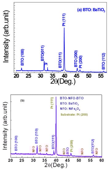
Figure 1.
X-ray diffraction pattern of (a) BTO and (b) (BTO/NFO/BTO) tri-layered thin film on substrate Pt/Ti/SiO2/Si at room temperature.
3.2. Raman Spectroscopy
Raman spectroscopy is a highly sensitive and non-destructive technique of probing the local crystal structure in materials. Raman spectra is an effective tool in probing the short-range disorder in the oxygen octahedral induced by Jahn–Teller distortion, etc., in oxide-based materials [32]. Figure 2 shows the room temperature measured Raman spectra of polycrystalline pure BaTiO3 and tri-layered BTO/NFO/BTO films. Room-temperature Raman spectra for pure BTO thin films have been characterized by tetragonal phase E1 (TO) ~58 cm−1, A1(TO1) ~184 cm−1, B1/E (TO+LO) ~305 cm−1 and asymmetric broader A1(TO2) ~257 cm−1, A1(TO3) ~517 cm−1, A1(LO)/E(LO) ~720 cm−1 modes, respectively. These latter three Raman modes are also present in paraelectric cubic phase, where they are much broader and more symmetrical. The A1(LO)/E(LO) mode is extremely broad and weak in cubic phase and often considered unique to the tetragonal phase [33,34]. These results are in complete agreement with pure tetragonal ferroelectric phased BTO bulk ceramics [33,34]. Trilayer structure BTO/NFO/BTO films have shown all the corresponding modes to that of Cubic inverse-spinel structure of NFO. As shown in Figure 2b for tri-layered BTO/NFO/BTO films, the BTO-related signals are barely visible and the Raman spectra are closely resembled to that of the pure NFO ferrite phase at room temperature. Our finding seems surprising as BaTiO3 forms the top layer of the tri-layered films, however from the experimental observation; it can be explained taking into account the different absorption behaviors of the two components. According to literature, there are five Raman active (A1g + Eg + 3T2g) modes in cubic spinel structure (space group Fd3m) [34]. NiFe2O4 ferrite is predominantly an inverse spinel. In general, the inverse spinel structure has the divalent cation occupying the octahedral sites and the trivalent cations are equally divided among the tetrahedral and remaining octahedral sites. In the NiFe2O4 spinel structure, the octahedral sites are occupied either by Ni or Fe ions [32]. All these five modes were observed at T2g ~(189-212) cm−1, Eg ~331 cm−1, T2g ~485 (NFO) cm−1, T2g ~530 (NFO) cm−1, A1g ~580 cm−1 (NFO), A1g ~702 (NFO) cm−1 along with these modes, an additional vibrational modes at 449 cm−1, A1g(2) ~590 cm−1, and at around 680 cm−1 is also evidenced, which is attributed to the presence of Fe3+ on the A-site of AB2O4 [32]. These additional shoulders peaks correspond to the inverse spinel structure and stem from Ni2+ and Fe3+, which show an ordered arrangement on the octahedral site [32]. All the observed peaks are in complete agreement with earlier reports [32,35,36,37].
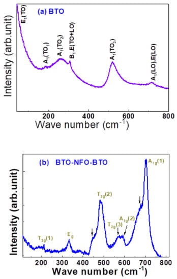
Figure 2.
Raman Spectrum of the (a) BTO and (b) (BTO/NFO/BTO) tri-layered thin film at room temperature.
3.3. Surface Morphology Study
The surface morphology of (BTO/NFO/BTO) tri-layered thin film system was observed by SEM is displayed in Figure 3a. The SEM micrographs of film have shown uniform distribution of grains throughout the surface of the sample examined. The grains and grain boundaries are well defined in the sample. Dense microstructure in the (BTO/NFO/BTO) tri-layered system is attributed suitable annealing temperature of the PLD deposited films. The average grain size of (BTO/NFO/BTO) tri-layered films is about 50 nm as shown in the figure. Grain growth in these films might be due to higher annealing temperature ~700 °C. From the SEM micrograph (Figure 3a), (BTO/NFO/BTO) tri-layered films did not show any obvious agglomeration.
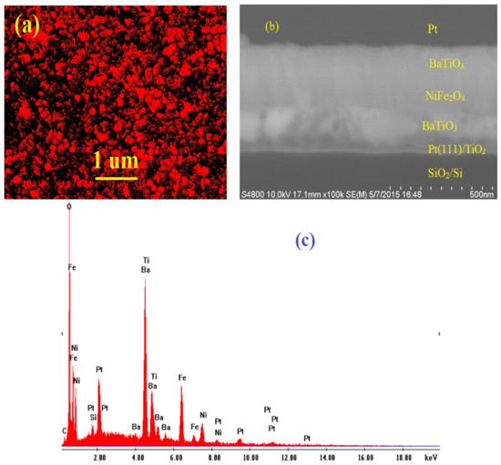
Figure 3.
(a) Surface FE-SEM image. (b) Cross-sectional SEM image. (c) EDX image of the grown (BTO/NFO/BTO) tri-layered thin film on substrate Pt(111)/Ti/SiO2/Si at room temperature.
Cross-sectional SEM photographs exhibit microstructures of the Pt/BTO/NFO/BTO films deposited on Pt/TiO2/SiO2/Si substrates as shown in Figure 3b. The cross sectional image also shows a dense polycrystalline and smooth surface on trilayer heterostructure. Energy dispersive spectroscopy (EDX) measurements revealed presence of each element (Ba, Ti, Ni, Fe, and O, respectively) present in the tri-layered films (Figure 3c), and SEM-EDX shows all the elemental peaks of (BTO/NFO/BTO) tri-layered along with peaks corresponding to Pt/TiO2/SiO2/Si substrate.
3.4. Leakage Current Behavior
The leakage current density-external electric field characteristics (J–E) of a metal–insulator–metal (MIM) capacitor employing BTO–NFO-BTO tri-layered film is shown in Figure 4. Note from Figure 4 that there is an exponential increase of current with voltage at low voltages, followed by a saturation region at high voltages. The voltage-step and the delay-time after applying each voltage-step were fixed at 0.5 V and 1s, respectively in the log J versus E measurements. Relatively low leakage current density is observed for the tri-layered thin films. The films exhibit low leakage current density (~10−9 A/cm2 at 0.3 MV/cm). Such reduction in leakage current density in these tri-layered films is correlated to higher annealing temperature (750 °C), and the completeness of perovskite phase formation in BTO–NFO-BTO films. At lower voltages, the leakage current is low and at high voltages the leakage current increases (~10−9 A/cm2 at 0.1 MV/cm) to (~10−6 A/cm2 at 0.3 MV/cm). The observed current density-electric filed (J-V) loops are noticeably symmetrical in nature. The possible symmetry of the two branches in the leakage currents might be because the positive and negative biases were applied on single pad and both the top electrode and bottom electrode were of same in nature, rather than using different top and bottom electrode pads. Here, in this case, we have platinum (Pt) as both top and bottom electrodes. The J–E relationship curve in the region of low electric field, the MIM structure was found to follow an ohmic conduction mechanism (J α En, n∼1) [21,22]. Whereas, in the region of higher electric field, the observed behavior may be attributed to Schottky type conduction and space charge-limited current (SCLC) conduction model (J α En, n > 1) [23,24].
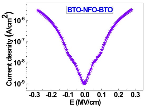
Figure 4.
Leakage current behavior (current density versus voltage) of (BTO/NFO/BTO) tri-layered thin film on substrate Pt/Ti/SiO2/Si at room temperature.
3.5. Dielectric Studies
Figure 5 shows the frequency dependent variation of dielectric constant (ε′) and dielectric loss or loss tangent (Tan δ = (ε′)/(ε′′)) of (BTO/NFO/BTO) thin film. The value of dielectric constant is found to decrease from 2145 (100 Hz) to 1414 (1 MHz) with increase in frequency. The dielectric constant (ε′) decreased rapidly with the increase in frequency at room temperature. This decrease in dielectric constant attributed to the reduction of space charge polarization effect. Dielectric loss is a dielectric relaxation process, and it represents the energy loss of the capacitor which occurs when the polarization of capacitor shifts behind the applied electric field caused by the grain boundaries. In a capacitor, dielectric loss originates from either from space charge migration that is the interfacial polarization contribution or due to the movement of the molecular dipoles (dipole loss) and the direct current (DC) conduction mechanism [11,14,15]. Dielectric loss (tan δ) increased with increase in frequency. The value of loss tangent value is found to be high (>0.25) in the region of high frequency region (1 MHz). At low frequency region tri-layered films have shown low dielectric loss (0.05). Dielectric properties have shown frequency dependence at room temperature. The high value of dielectric loss at a high frequency can be attributed to low resistivity of grain boundaries which is less effective than the grains [15].
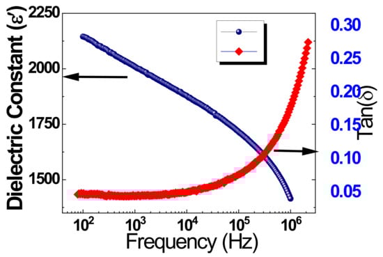
Figure 5.
Room temperature dielectric properties (dielectric constant and dielectric loss-tan δ) of (BTO/NFO/BTO) tri-layered thin film on substrate Pt/Ti/SiO2/Si.
3.6. Multiferroic Properties
To confirm the multiferroic properties of the (BTO/NFO/BTO) tri-layered thin films, we have measured the magnetization as a function of magnetic field and ferroelectric polarization as a function of electric field at room temperature.
3.6.1. M-H Hysteresis Curve
Figure 6 shows M-H hysteresis curve of the films deposited at 100 mTorr oxygen partial pressure. M-H hysteresis loops show a well-saturated ferromagnetic hysteretic behavior at room temperature. The magnetization curves present ferromagnetic ordering in NFO layers with a reasonably high saturation magnetization of ~16 emu/cm3 at room temperature. However, the observed value is less than the reported value of bulk NFO (~270 emu/cm3) [38]. The reduction in magnetization as compared to bulk NFO can be due to the small grain size of the films. The thermal energy in the samples has a significant effect on the magnetization. As the grain size decreases, thermal fluctuations increase, resulting in the reduction in magnetization. However, a higher magnetization (~78 emu/cm3) is recorded at 100 K. At low temperatures, the thermal energy is small so that the domains can easily be oriented along the applied field. Therefore, the increase in magnetization at low temperature can be attributed to the reorientation of the magnetic domains. The obtained saturation magnetization is comparable to the values previously reported in NFO-PZT heterostructures [26]. The coercivity of the sample is also found to increase when the temperature is decreased (from 130 Oe to 450 Oe). This too can be attributed to the reduction in thermal fluctuations.
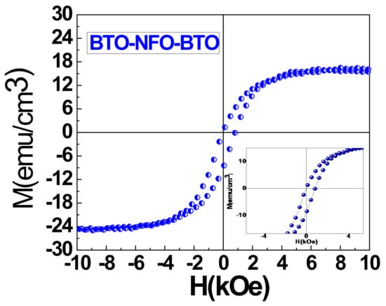
Figure 6.
Magnetization-Electric Field Hysteresis loop of (BTO/NFO/BTO) tri-layered thin film deposited at room temperature.
3.6.2. P-E Hysteresis Curve
Figure 7 shows the variation of electrical polarization (P) with the applied electric field (E) at different dc electric fields of (BTO/NFO/BTO) tri-layered films at room temperature at fixed frequency of 1 kHz. From the P-E loops, it has been observed that, a complete saturation is not observed in P-E which might be due to the existence of leakage currents at very high fields in the samples. The coercive field and remnant polarization increase with increase of electric field. This behavior suggests the ferroelectric nature of the samples. The ferroelectric nature of (BTO/NFO/BTO) tri-layered is demonstrated by a hysteresis loop between polarization (P) and applied electric field (E) obtained at different selected voltages (5 V–20 V) as shown in Figure 7, and the P-E hysteresis loops were measured at room temperature to estimate the maximum/spontaneous polarization of present samples. P-E hysteresis loops were measured up to a maximum electric field of 0.25 MV/cm. It can be observed from the Figure that the remnant polarization value is found to be 10.82 μCcm−2, while the maximum polarization value is equal to 15.75 μCcm−2. As the electric field increased from 0.55 MV/cm to 2.08 MV/cm, both maximum (saturation) polarization (Ps) and the remnant polarization (Pr) were increased. From the hysteresis loops it is observed that as the voltage increases, the P-E loop becomes slanted. The tri-layered film (BTO/NFO/BTO) also shows a rather asymmetric hysteresis behavior. From P-E hysteresis loops, it is also visible that there is a gap in the negative polarization axis. The gap is real and is caused by temporary memory that decays away in a few seconds. Therefore, the origin of the discontinuity in the P-E ferroelectric hysteresis loops observed here may be due to the polarization relaxation [38,39]. Similar effect is also observed in some of the reported on ferroelectric materials, where ferroelectric hysteresis loops exhibited such kind of discontinuity [38,39].
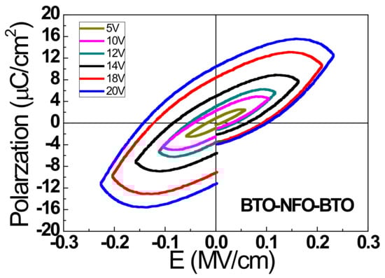
Figure 7.
Polarization-Electric Field Hysteresis loop of (BTO/NFO/BTO) tri-layered thin film deposited at room temperature.
3.6.3. Magnetoelectric (ME) Coupling Effect
We performed the ME characterization by the dynamic method at room temperature. In the dynamic ME method, an ac magnetic field δH generated by a solenoid, was superimposed onto a DC bias magnetic field Hbias and both were applied parallel to the sample plane and the change in the voltage δV across the tri-layered films was measured. The electric field E induced by δH and Hbias was measured using a lock-in amplifier (SRS Inc., SR830). In the present case, the small alternating magnetic field δH = 1 Oe (at frequency of 1 kHz) was superimposed and DC bias magnetic field Hbias varied from 0 kOe to ±3 kOe. The ME voltage coefficient (αE) is defined as αE = δE/δH = δV/ (δH t), where δV is the measured output voltage, δH is the applied ac magnetic field and t is the total thickness of the ferroelectric phase in the composite thin film.
As discussed in the above sections, the coexistence of ferroelectric and ferromagnetic behaviors in these films is also attributed to the measurable ME effect. Magnetoelectric (ME) effect in tri-layered BTO/NFO/BTO thin films is shown in Figure 8. The variation of magnetoelectric voltage coefficient (αE) with applied DC bias magnetic field (Hbias) is shown in figure. The (BTO/NFO/BTO) tri-layered thin films shows increase in αE with H to a maximum of 54.5 mV/cm Oe, at 500 Oe bias field followed by a sharp decrease to 23.6 mV/cm Oe at bias field of +3 kOe. This kind of behavior was also reported in single phase multiferroics, thin films (polycrystalline/epitaxial), and bi- and multilayered composite structures [10,40,41,42,43,44,45,46,47]. From the figure, it is observed that αE value does not decrease to zero value with increasing H. It is known that the ME voltage coefficients (αE) is directly proportional to the product of the piezomagnetic coefficient q = dλ/dH (where λ is the magnetostriction) and the piezoelectric coefficient. As the ME voltage arises due to magnetic–mechanical–electrical interactions, αE is proportional to q × d, its Hdc dependence is likely to follow the slope of λ vs Hbias of the magnetic material [45,46,47,48]. The magnetostriction of NFO is expected to be stronger at lower H in these heterostructures and decreases with increasing H. A similar type of magnetic field dependence of magnetostriction behavior of nickel ferrite has been reported [48]. In the present case, the increase or decrease of αE with Hbias is not similar with the application of positive and negative magnetic field. This asymmetry in the ME coefficient attributed to the existence of magnetic anisotropy in this tri-layered films and clamping of bottom ferroelectric layer with electrode coated substrate.
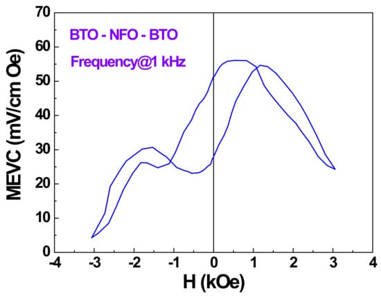
Figure 8.
Magnetoelectric (ME) effect in tri-layered BTO/NFO/BTO thin films.
Despite the observed ME coupling coefficient (αE) ~54.5 mV/cm Oe, in our BTO/NFO/BTO tri-layer thin film, is significantly higher than NFO/BTO epitaxial bilayer hetero structures(12.1 mV/cmOe), BTO/NFO/BTO tri-layers (32 mV/cmOe) and BTO/NFO/BTO/NFO/BTO penta layers (36 mV/cmOe), Pb(Zr0.4Ti0.6)O3–Ni0.8Zn0.2Fe2O4 multilayered thin films (15 mV/cmOe), and comparable with BiFeO3/BaTiO3 bilayer (61 mV/cmOe) [43,44,45,46,47,48]. One can observe that even at Hbias equal to zero, the tri-layer composite film exhibits an initial high αE value (i.e., 50 mV/cmOe) much larger than that of the bulk ferroelectric–ferromagnetic composite which is nearly close to zero. The zero-bias ME affect and the decrease in αE upon reversal of H direction indicate the possible presence of a uniaxial “built-in” magnetic field in the film.
4. Conclusions
In summary, in the present work we have successfully deposited high quality polycrystalline multiferroic BTO/NFO/BTO tri-layered thin films using the pulsed laser deposition method on the technologically important substrate Pt(111)/TiO2/SiO2/Si substrate. At an optimized deposition temperature ~750 °C and oxygen partial pressure~100 mTorr, tri-layered thin films have shown interesting multiferroic magnetoelectric properties. The XRD patterns have shown complete stoichiometry transfer from bulk ceramic target to that of films and showed no unwanted phase at the optimized growth temperature of 750 °C. These films have shown interesting ferroelectric properties with a maximum polarization of (~15.75 µCcm−2) and a remnant polarization value of ~10.82 µCcm−2 at about a maximum electric field of 0.3 MV/cm. Ferromagnetic properties include a maximum magnetization of 16 emu/cm3 at ~10 kOe. These films also displayed low leakage current behavior at room temperature. It could be concluded that chemical composition controlled BTO/NFO/BTO thin films can be used to optimize the multiferroic Magnetoelectric properties. The acquired results are interesting for spintronic applications.
Author Contributions
V.S.P. designed, synthesized bulk materials and PLD thin films and characterized XRD, Raman, ferroelectric, ferromagnetic measurements of the samples. V.S.P. wrote the complete manuscript. D.K.P., helped in characterization dielectric, ferroelectric measurements. K.M. helped in SEM, EDX measurements. G.S., S.N.B., N.V.P. helped in getting ferromagnetic, ME coupling data. D.B.C. and R.S.K. supervised this research work. All authors have read and agreed to the published version of the manuscript.
Funding
The author, V.S.P. acknowledges National Research Council (NRC) senior research associate fellowship program. This work was supported in part by the Air Force Office of Scientific Research and by the Air Force Research Laboratory, Directed Energy Directorate.
Data Availability Statement
Not applicable.
Acknowledgments
The author, VSP acknowledges National Research Council (NRC) senior research associate fellowship program. This work was supported in part by the Air Force Office of Scientific Research and by the Air Force Research Laboratory, Directed Energy Directorate. R.S.K. acknowledges DoD Project #FA9550-20-1-0064.
Conflicts of Interest
The authors declare no conflict of interest.
References
- Aizu, K. Possible species of ferromagnetic, ferroelectric, and ferroelastic crystals. Phys. Rev. B 1970, 2, 754. [Google Scholar] [CrossRef]
- Hill, N.A. Why are there so few magnetic ferroelectrics? J. Phys. Chem. B 2000, 104, 6694–6709. [Google Scholar] [CrossRef]
- Scott, J.F. Room-temperature multiferroic magnetoelectrics. NPG Asia Mater. 2013, 5, e72. [Google Scholar] [CrossRef] [Green Version]
- dos Santos, A.M.; Parashar, S.; Raju, A.R.; Zhao, Y.S.; Cheetham, A.K.; Rao, C.N.R. Evidence for the likely occurrence of magnetoferroelectricity in the simple perovskite, BiMnO3. Solid State Commun. 2002, 122, 49–52. [Google Scholar] [CrossRef]
- Wang, J.; Zhang, Y.; Ma, J.; Lin, Y.; Nan, C.W. Magnetoelectric behavior of BaTiO3 films directly grown on CoFe2O4 ceramics. J. Appl. Phys. 2008, 104, 014101. [Google Scholar] [CrossRef]
- Fiebig, M.; Lottermoser, T.; Fröhlich, D.; Goltsev, A.V.; Pisarev, R.V. Observation of coupled magnetic and electric domains. Nature 2002, 419, 818–820. [Google Scholar] [CrossRef] [PubMed]
- Laletsin, U.; Padubnaya, N.; Srinivasan, G.; Devreugd, C.P. Frequency dependence of magnetoelectric interactions in layered structures of ferromagnetic alloys and piezoelectric oxides. Appl. Phys. A 2004, 78, 33–36. [Google Scholar] [CrossRef] [Green Version]
- Jia, T.; Cheng, Z.; Zhao, H.; Kimura, H. Domain switching in single-phase multiferroics. Appl. Phys. Rev. 2018, 5, 021102. [Google Scholar] [CrossRef] [Green Version]
- Palkar, V.R.; John, J.; Pinto, R. Observation of saturated polarization and dielectric anomaly in magnetoelectric BiFeO3 thin films. Appl. Phys. Lett. 2002, 80, 1628–1630. [Google Scholar] [CrossRef]
- Wang, J.; Neaton, J.B.; Zheng, H.; Nagarajan, V.; Ogale, S.B.; Liu, B.; Viehland, D.; Vaithyanathan, V.; Schlom, D.G.; Waghmare, U.V.; et al. Epitaxial BiFeO3 Multiferroic Thin Film Heterostructures. Science 2003, 299, 1719–1722. [Google Scholar] [CrossRef]
- Puli, V.S.; Pradhan, D.K.; Katiyar, R.K.; Coondoo, I.; Panwar, N.; Misra, P.; Chrisey, D.B.; Scott, J.F.; Katiyar, R.S. Photovoltaic effect in transition metal modified polycrystalline BiFeO3 thin films. J. Phys. D Appl. Phys. 2014, 47, 075502. [Google Scholar] [CrossRef] [Green Version]
- Lente, M.H.; Guerra, J.D.S.; de Souza, G.K.S.; Fraygola, B.M.; Raigoza, C.F.V.; Garcia, D.; Eiras, J.A. Nature of the magnetoelectric coupling in multiferroic Pb(Fe1/2Nb1/2)O3 ceramics. Phys. Rev. B 2008, 78, 054109. [Google Scholar] [CrossRef]
- Kleemann, W.; Shvartsman, V.; Borisov, P.; Kania, A. Coexistence of Antiferromagnetic and Spin Cluster Glass Order in the Magnetoelectric Relaxor Multiferroic PbFe0.5Nb0.5O3. Phys. Rev. Lett. 2010, 105, 257202. [Google Scholar] [CrossRef]
- Pradhan, D.K.; Sahoo, S.; Barik, S.K.; Puli, V.S.; Misra, P.; Katiyar, R.S. Studies on magnetoelectric coupling in PFN-NZFO composite at room temperature. J. Appl. Phys. 2014, 115, 194105. [Google Scholar] [CrossRef]
- Pradhan, D.K.; Kumari, S.; Vasudevan, R.K.; Dugu, S.; Das, P.T.; Puli, V.S.; Pradhan, D.K.; Kalinin, S.V.; Katiyar, R.S.; Rack, P.D.; et al. Room temperature multiferroicity and magnetodielectric coupling in 0–3 composite thin films. J. Appl. Phys. 2020, 127, 194104. [Google Scholar] [CrossRef]
- da Silveira Lacerda, L.H.; Ribeiro, R.A.P.; Lazaro, S.R. Magnetic, electronic, ferroelectric, structural and topological analysis of AlFeO3, FeAlO3, FeVO3, BiFeO3 and PbFeO3 materials: Theoretical evidences of magnetoelectric coupling. J. Magn. Magn. Mater. 2019, 480, 199–208. [Google Scholar] [CrossRef]
- Li, Y.; Wang, Y.G.; Wang, N.; Wang, F.L.; Jain, A. Magnetoelectric (1-x)AlFeO3-xBaTiO3 solid solutions with ferroelectric relaxor behavior near room temperature. Ceram. Int. 2020, 46, 7930–7938. [Google Scholar] [CrossRef]
- Shastry, S.; Srinivasan, G.; Bichurin, M.I.; Petrov, V.M.; Tatarenko, A.S. Microwave magnetoelectric effects in single crystal bilayers of yttrium iron garnet and lead magnesium niobate-lead titanate. Phys. Rev. B 2004, 70, 064416. [Google Scholar] [CrossRef] [Green Version]
- Zheng, H.; Wang, J.; Lofland, S.E.; Ma, Z.; Mohaddes-Ardabili, L.; Zhao, T.; Salamanca-Riba, L.; Shinde, S.R.; Ogale, S.B.; Bai, F.; et al. Multiferroic BaTiO3-CoFe2O4 nanostructures. Science 2004, 303, 661–663. [Google Scholar] [CrossRef] [PubMed] [Green Version]
- Pradhan, D.K.; Kumari, S.; Vasudevan, R.K.; Strelcov, E.; Puli, V.S.; Pradhan, D.K.; Kumar, A.; Gregg, J.M.; Pradhan, A.K.; Kalinin, S.V.; et al. Exploring the Magnetoelectric Coupling at the Composite Interfaces of FE/FM/FE Heterostructures. Sci. Rep. 2018, 8, 17381. [Google Scholar] [CrossRef]
- Moreira dos Santos, A.; Cheetham, A.K.; Atou, T.; Syono, Y.; Yamaguchi, Y.; Ohoyama, K.; Chiba, H.; Rao, C.N.R. Orbital ordering as the determinant for ferromagnetism in biferroic BiMnO3. Phys. Rev. B 2002, 66, 064425. [Google Scholar] [CrossRef]
- Puli, V.S.; Pradhan, D.K.; Gollapudi, S.; Coondoo, I.; Panwar, N.; Adireddy, S.; Chrisey, D.B.; Katiyar, R.S. Magnetoelectric coupling effect in transition metal modified polycrystalline BiFeO3 thin films. J. Magn. Magn. Mater. 2014, 369, 9–13. [Google Scholar] [CrossRef]
- Panwar, N.; Coondoo, I.; Tomar, A.; Kholkin, A.L.; Puli, V.S.; Katiyar, R.S. Nanoscale piezoresponse and magnetic studies of multiferroic Co and Pr co-substituted BFO thin films. Mater. Res. Bull. 2012, 47, 4240–4245. [Google Scholar] [CrossRef]
- Choi, T.; Horibe, Y.; Yi, H.T.; Choi, Y.J.; Wu, W.D.; Cheong, S.W. Insulating interlocked ferroelectric and structural antiphase domain walls in multiferroic YMnO3. Nat. Mater. 2010, 9, 253–258. [Google Scholar] [CrossRef]
- Jang, S.Y.; Lee, D.; Lee, J.-H.; Murugavel, P.; Chung, J.-S.; Jin-Seok, C.; Yup, J.S.; Daesu, L.; Jung-Hyuk, L.; Pattukkannu, M. Ferroelectric Properties of Multiferroic Hexagonal ErMnO3 Thin Films. J. Korean Phys. Soc. 2009, 55, 841–845. [Google Scholar] [CrossRef]
- Kimura, T.; Goto, T.; Shintani, H.; Ishizaka, K.; Arima, T.; Tokura, Y. Magnetic control of ferroelectric polarization. Nature 2003, 426, 55–58. [Google Scholar] [CrossRef]
- Zhao, H.Y.; Kimura, H.; Cheng, Z.X.; Osada, M.; Wang, J.L.; Wang, X.L.; Dou, S.X.; Liu, Y.; Yu, J.D.; Matsumoto, T.; et al. Large magnetoelectric coupling in magnetically short-range ordered Bi5Ti3FeO15 film. Sci. Rep. 2014, 4, 5255. [Google Scholar] [CrossRef] [PubMed] [Green Version]
- Imai, A.; Cheng, X.; Xin, H.L.; Eliseev, E.A.; Morozovska, A.N.; Kalinin, S.V.; Takahashi, R.; Lippmaa, M.; Matsumoto, Y.; Nagarajan, V. Epitaxial Bi5Ti3FeO15-CoFe2O4 pillar-matrix multiferroic nanostructures. ACS Nano 2013, 7, 11079–11086. [Google Scholar] [CrossRef] [PubMed]
- Sepelak, V.; Baabe, D.; Mienert, D.; Schultze, D.; Krumeich, F.; Litterst, F.J.; Becker, K.D. Evolution of structure and magnetic propeties with annealing temperature in nanoscale high-energy-milled nickel ferrite. J. Magn. Magn. Mater. 2003, 257, 377–386. [Google Scholar] [CrossRef]
- Powder Diffraction File, Joint Committee on Powder Diffraction Standards. International Centre for Diffraction Data, Cards. 2004, 10-325 and 5-626. Available online: https://www.icdd.com/pdfsearch/ (accessed on 31 August 2021).
- Gonçalves, J.R.; Barbosa, J.; Sá, P.; Mendes, J.A.; Rolo, A.G.; Almeida, B.G. Structural and Raman characterization of nanogranular BaTiO3-NiFe2O4 thin films deposited by laser ablation on Si/Pt substrates. Phys. Status Solidi C 2010, 7, 2720–2723. [Google Scholar] [CrossRef]
- Ahlawat, A.; Sathe, V.G. Raman study of NiFe2O4 nanoparticles, bulk and films: Effect of laser power. J. Raman Spectrosc. 2011, 42, 1087–1094. [Google Scholar] [CrossRef]
- Puli, V.S.; Pradhan, D.K.; Riggs, B.C.; Adireddy, S.; Katiyar, R.S.; Chrisey, D.B. Synthesis and characterization of lead-free ternary component BST–BCT–BZT ceramic capacitors. J. Adv. Dielectr. 2014, 4, 1450014. [Google Scholar] [CrossRef]
- Puli, V.S.; Li, P.; Adireddy, S.; Chrisey, D.B. Crystal structure, dielectric, ferroelectric and energy storage properties of La-doped BaTiO3 semiconducting ceramics. J. Adv. Dielectr. 2015, 5, 1550027. [Google Scholar] [CrossRef]
- Iliev, M.N.; Mazumdar, D.; Ma, J.X.; Gupta, A.; Rigato, F.; Fontcuberta, J. Monitoring B-site ordering and strain relaxation in NiFe2O4 epitaxial films by polarized Raman spectroscopy. Phys. Rev. B 2011, 83, 014108. [Google Scholar] [CrossRef] [Green Version]
- Chandramohan, P.; Srinivasan, M.P.; Velmurugan, S.; Narasimhan, S.V. Cation distribution and particle size effect on Raman spectrum of CoFe2O4. J. Solid State Chem. 2011, 184, 89–96. [Google Scholar] [CrossRef]
- Quandt, N.; Roth, R.; Syrowatka, F.; Steimecke, M.; Ebbinghaus, S.G. Spin-Coating and Characterization of Multiferroic MFe2O4 (M=Co, Ni)/BaTiO3 Bilayers. J. Solid State Chem. 2016, 233, 82–89. [Google Scholar] [CrossRef]
- Puli, V.S.; Pradhan, D.K.; Adireddy, S.; Martínez, R.V.; Silwal, P.; Scott, J.F.; Ramana, C.V.; Chrisey, D.B.; Katiyar, R.S. Nanoscale polarisation switching and leakage currents in (Ba0.955Ca0.045)(Zr0.17Ti0.83)O3 epitaxial thin films. J. Phys. D Appl. Phys. 2015, 48, 355502. [Google Scholar] [CrossRef]
- Puli, V.S.; Pradhan, D.K.; Coondoo, I.; Panwar, N.; Adireddy, S.; Luo, S.; Katiyar, R.S.; Chrisey, D.B. Observation of Large enhancement in energy-storage properties of lead-free polycrystalline 0.5BaZr0.2Ti0.8O3-0.5Ba0.7Ca0.3TiO3 ferroelectric thin films. J. Phys. D Appl. Phys. 2019, 52, 255304. [Google Scholar] [CrossRef]
- Kumari, S.; Kimura, H.; Cheng, Z.; Osada, M.; Wang, J.; Wang, X.; Dou, S.X.; Liu, Y.; Yu, J.; Matsumoto, T.; et al. Dielectric Anomalies Due to Grain Boundary Conduction in Chemically Substituted BiFeO3. J. Appl. Phys. 2015, 117, 114102. [Google Scholar] [CrossRef] [Green Version]
- Cheng, Z.X.; Wang, X.L.; Zhao, H.Y.; Kimura, H. Lead-free potassium bismuth titanate thin film with complex Aurivillius layer structure. J. Appl. Phys. 2010, 107, 084105. [Google Scholar] [CrossRef] [Green Version]
- Deng, C.; Zhang, Y.; Ma, J.; Lin, Y.; Nan, C.-W. Magnetic-electric properties of epitaxial multiferroic NiFe2O4—BaTiO3 heterostructure. J. Appl. Phys. 2007, 102, 074114. [Google Scholar] [CrossRef]
- Liu, J.; Zhang, Y.; Lin, Y.; Nan, C.-W. Magnetoelectric coupling in BaTiO3/(NiFe2O4/BaTiO3)n (n = 1, 2, 3, 4) multilayered thin films. J. Appl. Phys. 2009, 105, 083915. [Google Scholar] [CrossRef]
- Ryu, S.; Park, J.H.; Jang, H.M. Magnetoelectric coupling of [00l]-oriented Pb (Zr0.4Ti0.6)O3–Ni0.8Zn0.2Fe2O4 multilayered thin films. Appl. Phys. Lett. 2007, 91, 142910. [Google Scholar] [CrossRef] [Green Version]
- Gupta, R.; Chaudhary, S.; Kotnala, R.K. Interfacial Charge Induced Magnetoelectric Coupling at BiFeO3/BaTiO3 Bilayer Interface. ACS Appl. Mater. Interfaces 2015, 7, 8472–8479. [Google Scholar] [CrossRef] [PubMed]
- Ma, J.; Hu, J.; Li, Z.; Nan, C.-W. Recent Progress in Multiferroic Magnetoelectric Composites: From Bulk to Thin Films. Adv. Mater. 2011, 23, 1062–1087. [Google Scholar] [CrossRef] [PubMed]
- Vaz, C.A.F.; Hoffman, J.; Ahn, C.H.; Ramesh, R. Magnetoelectric Coupling Effects in Multiferroic Complex Oxide Composite Structures. Adv. Mater. 2010, 22, 2900–2918. [Google Scholar] [CrossRef]
- Srinivasan, G.; Rasmussen, E.T.; Gallegos, J.; Bokhan, Y.I.; Laletin, V.M. Magnetoelectric bilayer and multilayer structures of magnetostrictive and piezoelectric oxides. Phys. Rev. B 2001, 64, 214408. [Google Scholar] [CrossRef]
Publisher’s Note: MDPI stays neutral with regard to jurisdictional claims in published maps and institutional affiliations. |
© 2021 by the authors. Licensee MDPI, Basel, Switzerland. This article is an open access article distributed under the terms and conditions of the Creative Commons Attribution (CC BY) license (https://creativecommons.org/licenses/by/4.0/).