In-Situ Annealing and Hydrogen Irradiation of Defect-Enhanced Germanium Quantum Dot Light Sources on Silicon

 ,
,  , , and
Abstract
1. Introduction
2. Materials and Methods
3. Results and Discussion
3.1. DEQD Nanostructures
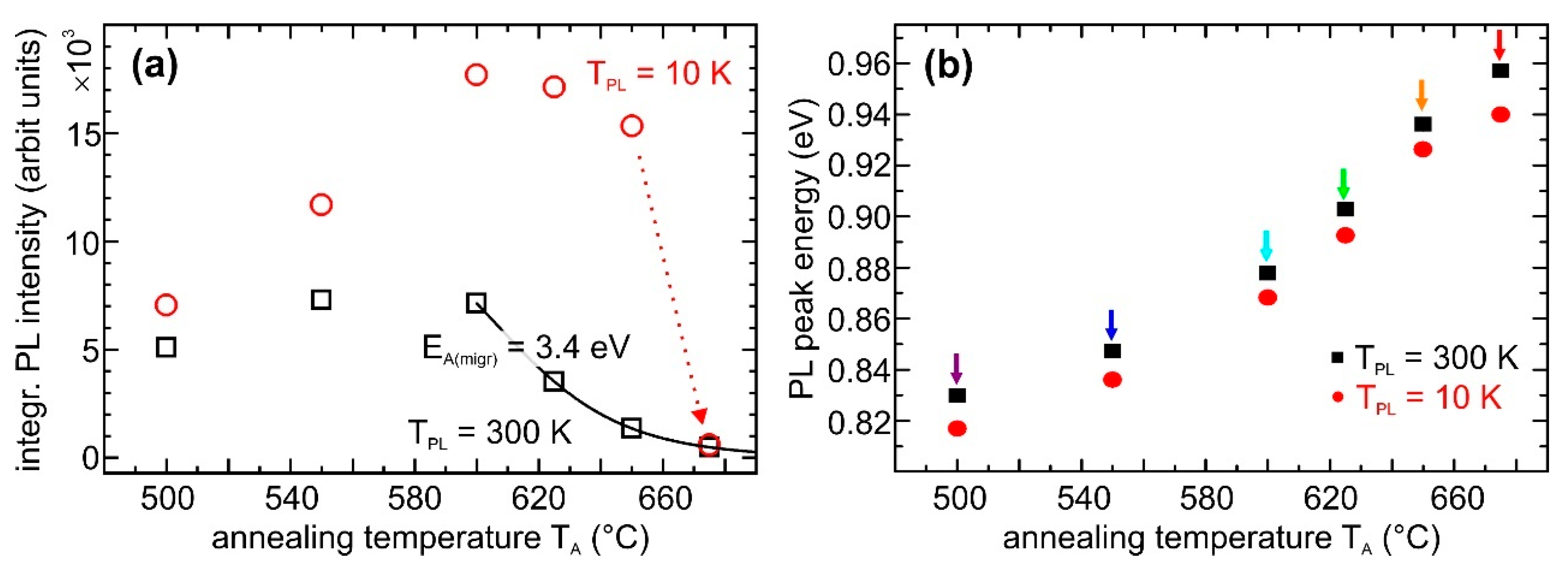
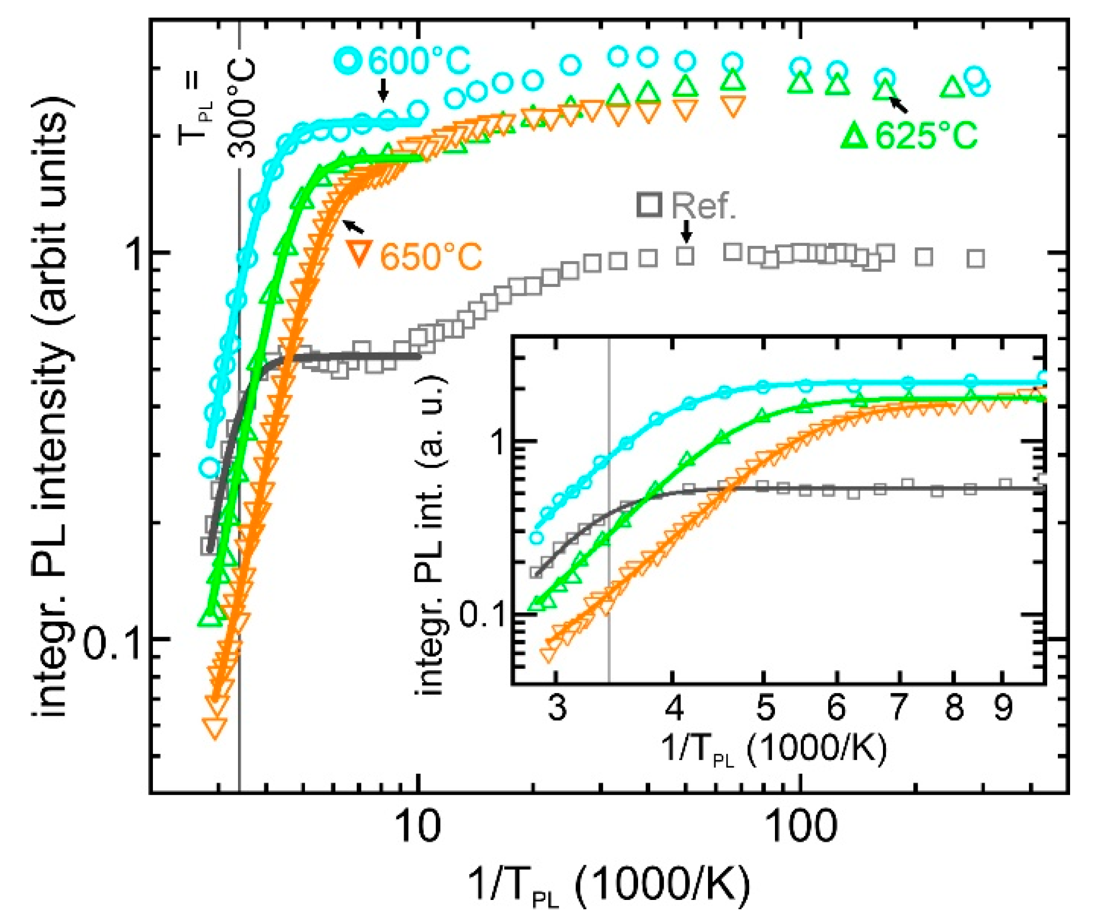
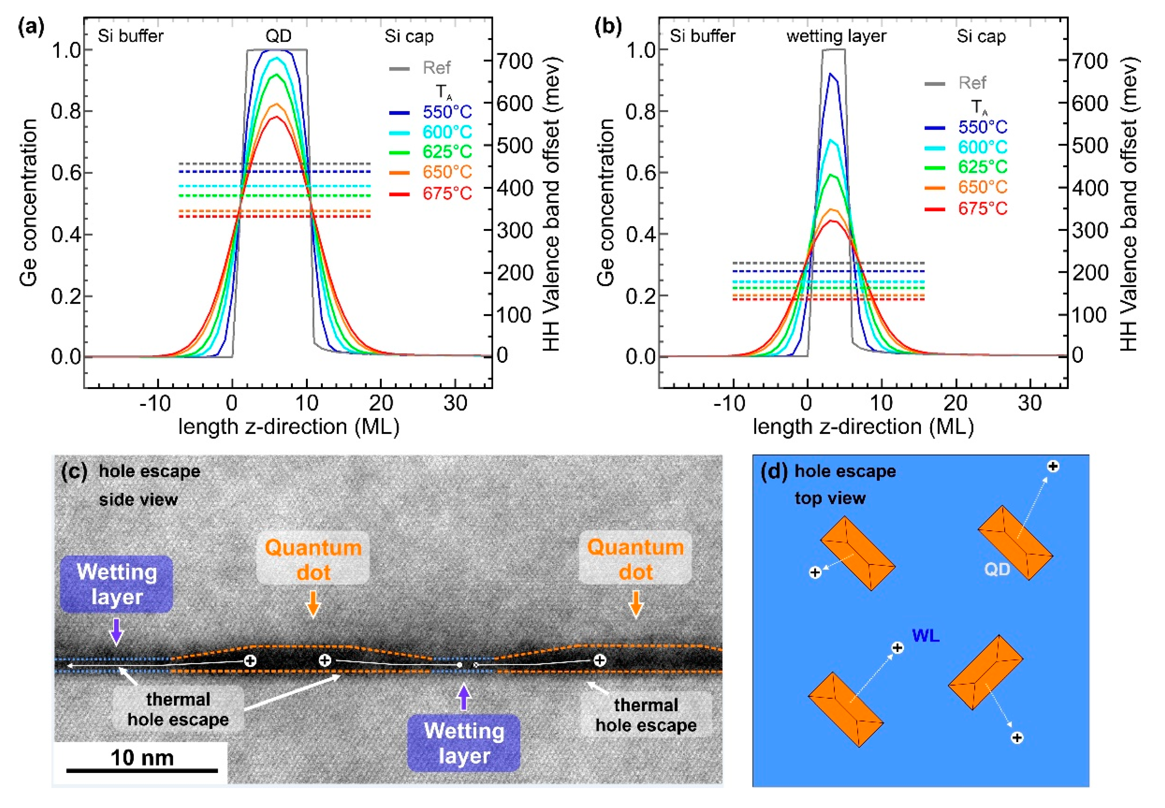
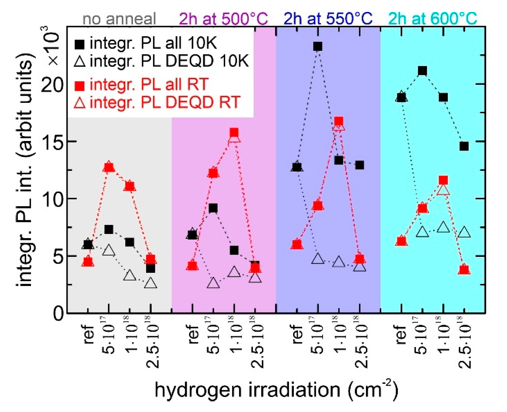
3.2. In-Situ Annealing of DEQDs
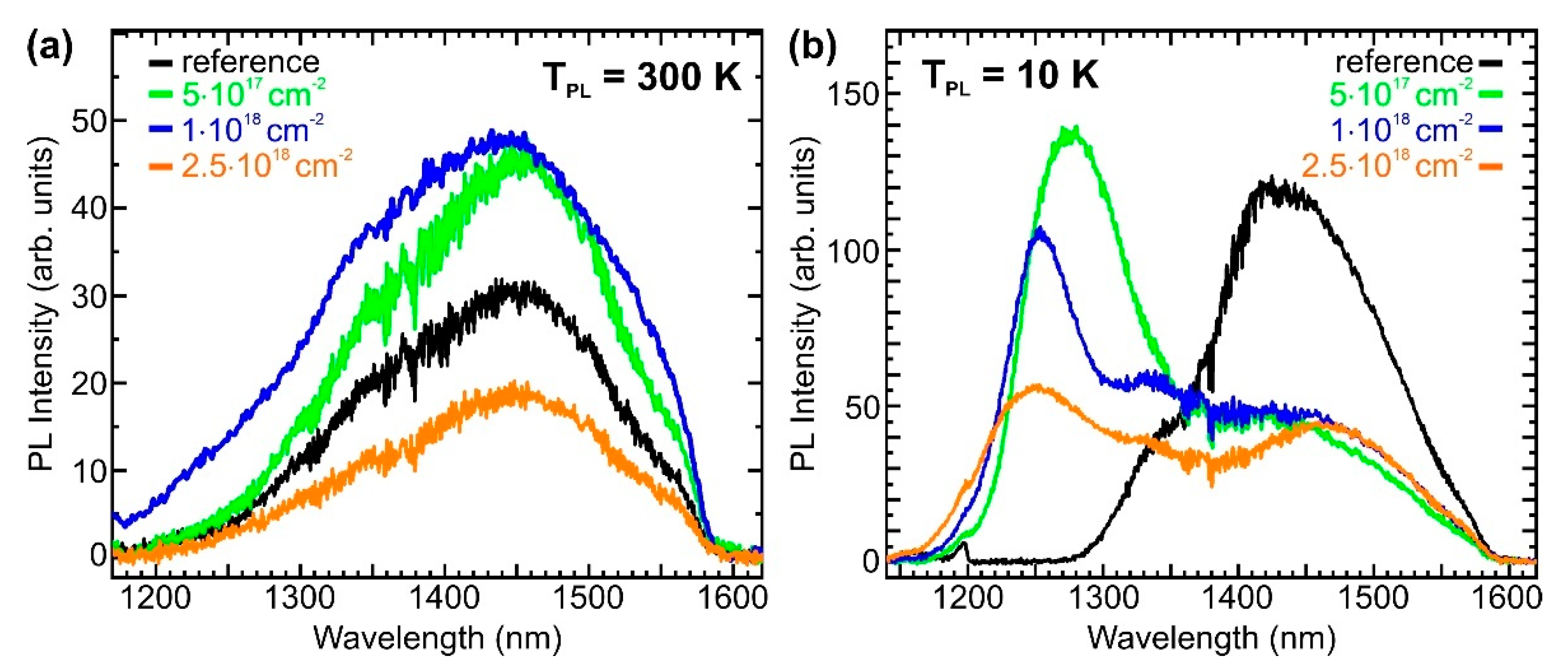
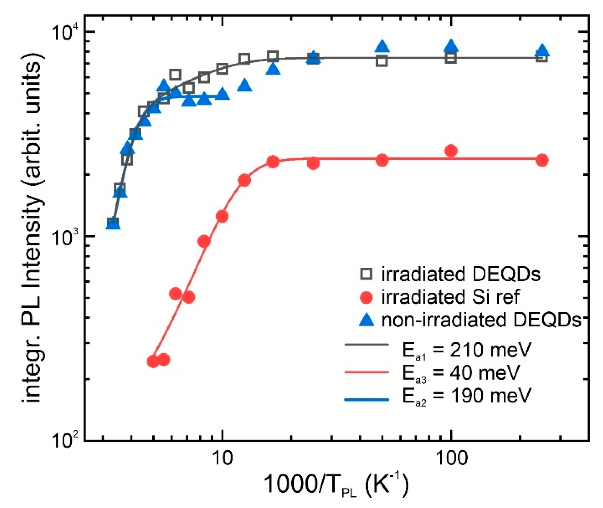
3.3. H-Irradiation Treatment of DEQDs
4. Conclusions
Author Contributions
Funding
Acknowledgments
Conflicts of Interest
Appendix A

References
- Pavesi, L.; Lockwood, D.J. Photonics III: Systems and Applications; Springer: Berlin/Heidelberg, Germany, 2016. [Google Scholar]
- Reed, G.T.; Knights, A.P. Silicon Photonics: An Introduction; John Wiley: Chichester, UK, 2004. [Google Scholar]
- Tsybeskov, L.; Lockwood, D.J.; Ichikawa, M. Silicon photonics: CMOS going optical. Proc. IEEE 2009, 97, 1161–1165. [Google Scholar] [CrossRef]
- Baldassarre, L.; Sakat, E.; Frigerio, J.; Samarelli, A.; Gallacher, K.; Calandrini, E.; Isella, G.; Paul, D.J.; Ortolani, M.; Biagioni, P.; et al. Midinfrared plasmon-enhanced spectroscopy with germanium antennas on silicon substrates. Nano Lett. 2015, 15, 7225. [Google Scholar] [CrossRef] [PubMed]
- Chen, S.; Li, W.; Wu, J.; Jiang, Q.; Tang, M.; Shutts, S.; Elliott, S.N.; Sobiesierski, A.; Seeds, A.J.; Ross, I.; et al. Electrically pumped continuous-wave III–V quantum dot lasers on silicon. Nat. Photonics 2016, 10, 307–311. [Google Scholar] [CrossRef]
- Wang, T.; Liu, H.; Lee, A.; Pozzi, F.; Seeds, A. 1.3-μm InAs/GaAs quantum-dot lasers monolithically grown on Si substrates. Opt. Express 2011, 19, 11381–11386. [Google Scholar] [CrossRef] [PubMed]
- Shi, Y.; Wang, Z.; Van Campenhout, J.; Pantouvaki, M.; Guo, W.; Kunert, B.; Van Thourhout, D. Optical pumped InGaAs/GaAs nano-ridge laser epitaxially grown on a standard 300-mm Si wafer. Optica 2017, 4, 1468–1473. [Google Scholar] [CrossRef]
- Armand Pilon, F.T.; Lyasota, A.; Niquet, Y.-M.; Reboud, V.; Calvo, V.; Pauc, N.; Widiez, J.; Bonzon, C.; Hartmann, J.M.; Chelnokov, A.; et al. Lasing in strained germanium microbridges. Nat. Commun. 2019, 10, 2724. [Google Scholar] [CrossRef]
- Wirths, S.; Geiger, R.; von den Driesch, N.; Mussler, G.; Stoica, T.; Mantl, S.; Ikonic, Z.; Luysberg, M.I.; Chiussi, S.; Hartmann, J.-M.; et al. Lasing in direct-bandgap GeSn alloy grown on Si. Nat. Photonics 2015, 9, 88–92. [Google Scholar] [CrossRef]
- Grydlik, M.; Hackl, F.; Groiss, H.; Glaser, M.; Halilovic, A.; Fromherz, T.; Jantsch, W.; Schäffler, F.; Brehm, M. Lasing from glassy Ge quantum dots in crystalline Si. ACS Photonics 2016, 3, 298–303. [Google Scholar] [CrossRef]
- Persichetti, L.; Montanari, M.; Ciano, C.; Di Gaspare, L.; Ortolani, M.; Baldassarre, L.; Zoellner, M.; Mukherjee, S.; Moutanabbir, O.; Capellini, G.; et al. Intersubband transition engineering in the conduction band of asymmetric coupled Ge/SiGe quantum wells. Crystals 2020, 10, 179. [Google Scholar] [CrossRef]
- Zhou, Y.; Dou, W.; Du, W.; Ojo, S.; Tran, H.; Ghetmiri, S.A.; Liu, J.; Sun, G.; Soref, R.; Margetis, J.; et al. Optically pumped GeSn lasers operating at 270 K with broad waveguide structures on Si. ACS Photonics 2019, 6, 1434–1441. [Google Scholar] [CrossRef]
- Cornet, C.; Léger, Y.; Robert, C. Integrated Lasers on Si; ISTE-Elsevier: Amsterdam, The Netherlands, 2016. [Google Scholar]
- Takeuchi, H.; Wung, A.; Sun, X.; Howe, R.T.; King, T.-J. Thermal budget limits of quarter-micrometer foundry CMOS for post-processing MEMS devices. IEEE Trans. Electron Devices 2005, 52, 2081–2086. [Google Scholar] [CrossRef]
- Xiao, H. Introduction to Semiconductor Manufacturing Technology; Prentice-Hall: Upper Saddle River, NJ, USA, 2001. [Google Scholar]
- Hamann, H.F.; Weger, A.; Lacey, J.A.; Hu, Z.; Bose, P.; Cohen, E.; Wakil, J. Hotspot-limited microprocessors: Direct temperature and power distribution measurements. IEEE J. Solid-State Circuits 2007, 42, 56–65. [Google Scholar] [CrossRef]
- Bimberg, D.; Kirstaedter, N.; Ledentsov, N.N.; Alferov, Z.I.; Kop’ev, P.S.; Ustinov, V.M. InGaAs–GaAs quantum-dot lasers. IEEE J. Sel. Top. Quantum Electron. 1997, 3, 196–205. [Google Scholar] [CrossRef]
- Grydlik, M.; Lusk, M.T.; Hackl, F.; Polimeni, A.; Fromherz, T.; Jantsch, W.; Schäffler, F.; Brehm, M. Laser level scheme of self-interstitials in epitaxial Ge dots encapsulated in Si. Nano Lett. 2016, 16, 6802–6807. [Google Scholar] [CrossRef] [PubMed]
- Brehm, M.; Grydlik, M. Site-controlled and advanced epitaxial Ge/Si quantum dots: Fabrication, properties, and applications. Nanotechnology 2017, 28, 392001. [Google Scholar] [CrossRef]
- Groiss, H.; Spindlberger, L.; Oberhumer, P.; Schäffler, F.; Fromherz, T.; Grydlik, M.; Brehm, M. Photoluminescence enhancement through vertical stacking of defect-engineered Ge on Si quantum dots. Semicond. Sci. Technol. 2017, 32, 02LT01. [Google Scholar] [CrossRef]
- Rauter, P.; Spindlberger, L.; Schäffler, F.; Fromherz, T.; Freund, J.; Brehm, M. Room-temperature group-IV LED based on defect-enhanced Ge quantum dots. ACS Photonics 2018, 5, 431–438. [Google Scholar] [CrossRef]
- Hallam, B.; Chen, D.; Kim, M.; Stefani, B.; Hoex, B.; Abbott, M.; Wenham, S. The role of hydrogenation and gettering in enhancing the efficiency of next-generation Si solar cells: An industrial perspective. Phys. Status Solidi A 2017, 214, 1700305. [Google Scholar] [CrossRef]
- Cartier, E.; Stathis, J.H.; Buchanan, D.A. Passivation and depassivation of silicon dangling bonds at the Si/SiO2 interface by atomic hydrogen. Appl. Phys. Lett. 1993, 63, 1510. [Google Scholar] [CrossRef]
- Kern, W. The evolution of silicon wafer cleaning technology. J. Electrochem. Soc. 1990, 137, 1887–1892. [Google Scholar] [CrossRef]
- Tomita, H.; Kikuchi, T.; Furuya, K. Hydrogen desorption behaviors of HF-treated silicon wafer. Jpn. J. Appl. Phys. 1991, 30, 897. [Google Scholar] [CrossRef]
- Mo, Y.-W.; Savage, D.E.; Swartzentruber, B.S.; Lagally, M.G. Kinetic pathway in Stranski-Krastanov growth of Ge on Si (001). Phys. Rev. Lett. 1990, 65, 1020. [Google Scholar] [CrossRef] [PubMed]
- Capellini, G.; De Seta, M.; Evangelisti, F. Influence of the growth parameters on self-assembled Ge islands on Si(100). Mater. Sci. Eng. B 2001, 89, 184–187. [Google Scholar] [CrossRef]
- Brehm, M.; Montalenti, F.; Grydlik, M.; Vastola, G.; Lichtenberger, H.; Hrauda, N.; Beck, M.J.; Fromherz, T.; Schäffler, F.; Miglio, L.; et al. Key role of the wetting layer in revealing the hidden path of Ge/Si (001) Stranski-Krastanow growth onset. Phys. Rev. B 2009, 80, 205321. [Google Scholar] [CrossRef]
- Mazzucato, S.; Nardin, D.; Capizzi, M.; Polimeni, A.; Frova, A.; Seravalli, L.; Franchi, S. Defect passivation in strain engineered InAs/(InGa) As quantum dots. Mater. Sci. Eng. C 2005, 25, 830–834. [Google Scholar] [CrossRef]
- Felici, M.; Polimeni, A.; Salviati, G.; Lazzarini, L.; Armani, N.; Masia, F.; Capizzi, M.; Martelli, F.; Lazzarino, M.; Bais, G.; et al. In-plane bandgap engineering by modulated hydrogenation of dilute nitride semiconductors. Adv. Mater. 2006, 18, 1993–1997. [Google Scholar] [CrossRef]
- Klar, P.J.; Grüning, H.; Güngerich, M.; Heimbrodt, W.; Koch, J.; Torunski, T.; Stolz, W.; Polimeni, A.; Capizzi, M. Global changes of the band structure and the crystal lattice of Ga (N, As) due to hydrogenation. Phys. Rev. B 2003, 67, 121206. [Google Scholar] [CrossRef]
- Tedeschi, D.; Blundo, E.; Felici, M.; Pettinari, G.; Liu, B.; Yildrim, T.; Petroni, E.; Zhang, C.; Zhu, Y.; Sennato, S.; et al. Controlled micro/nanodome formation in proton-irradiated bulk transition-metal dichalcogenides. Adv. Mater. 2019, 31, 1903795. [Google Scholar] [CrossRef]
- Spindlberger, L.; Prucnal, S.; Aberl, J.; Brehm, M. Thermal stability of defect-enhanced Ge on Si quantum dot luminescence upon millisecond flash lamp annealing. Phys. Status Solidi A 2019, 216, 1900307. [Google Scholar] [CrossRef]
- Capellini, G.; De Seta, M.; Evangelisti, F. SiGe intermixing in Ge/Si (100) islands. Appl. Phys. Lett. 2001, 78, 303–305. [Google Scholar] [CrossRef]
- Brehm, M.; Grydlik, M.; Lichtenberger, H.; Fromherz, T.; Hrauda, N.; Jantsch, W.; Schäffler, F.; Bauer, G. Quantitative determination of Ge profiles across SiGe wetting layers on Si (001). Appl. Phys. Lett. 2008, 93, 121901. [Google Scholar] [CrossRef]
- Godbey, D.G.; Ancona, M.G. Modeling of Ge segregation in the limits of zero and infinite surface diffusion. J. Vac. Sci. Technol. A 1997, 15, 976. [Google Scholar] [CrossRef]
- Chen, P.; Etzelstorfer, T.; Hackl, F.; Katcho, N.A.; Chang, H.-T.; Nausner, L.; Lee, S.-W.; Fromherz, T.; Stangl, J.; Schmidt, O.G.; et al. Evolution of thermal, structural, and optical properties of SiGe superlattices upon thermal treatment. Phys. Status Solidi A 2016, 213, 533–540. [Google Scholar] [CrossRef]
- Majewski, J.A.; Birner, S.; Trellakis, A.; Sabathil, M.; Vogl, P. Advances in the theory of electronic structure of semiconductors. Phys. Status Solidi C 2004, 1, 2003. [Google Scholar] [CrossRef]
- Grydlik, M.; Brehm, M.; Hackl, F.; Groiss, H.; Fromherz, T.; Schäffler, F.; Bauer, G. Inverted Ge islands in {111} faceted Si pits—A novel approach towards SiGe islands with higher aspect ratio. New J. Phys. 2010, 12, 063002. [Google Scholar] [CrossRef]
- Kube, R.; Bracht, H.; Lundsgaard Hansen, J.; Nylandsted Larsen, A.; Haller, E.E.; Paul, S.; Lerch, W. Simultaneous diffusion of Si and Ge in isotopically controlled Si1−xGex heterostructures. Mater. Sci. Semicond. Process. 2008, 11, 378–383. [Google Scholar] [CrossRef]
- Kube, R.; Bracht, H.; Lundsgaard Hansen, J.; Nylandsted Larsen, A.; Haller, E.E.; Paul, S.; Lerch, W. Composition dependence of Si and Ge diffusion in relaxed Si1−xGex alloys. J. Appl. Phys. 2010, 107, 073520. [Google Scholar] [CrossRef]
- Heitjans, P.; Karger, J. Diffusion in Condensed Matter: Methods, Materials, Models, 2nd ed.; Birkhauser: Basel, Switzerland, 2005; pp. 19–65. [Google Scholar]
- Wang, S.; Mai, L.; Ciesla, A.; Hameiri, Z.; Payne, D.; Chan, C.; Hallam, B.; Chong, C.M.; Ji, J.; Shi, Z.; et al. Advanced passivation of laser-doped and grooved solar cells. Sol. Energy Mater. Sol. Cells 2019, 193, 403–410. [Google Scholar] [CrossRef]
- Fujimori, S.; Nagai, R.; Ikeda, M.; Makihara, K.; Miyazaki, S. Effect of H2-dilution in Si-cap formation on photoluminescence intensity of Si quantum dots with Ge core. Jpn. J. Appl. Phys. 2019, 58, SIIA01. [Google Scholar] [CrossRef]
- Hackl, F.; Grydlik, M.; Brehm, M.; Groiss, H.; Schäffler, F.; Fromherz, T.; Bauer, G. Microphotoluminescence and perfect ordering of SiGe islands on pit-patterned Si (001) substrates. Nanotechnology 2011, 22, 165302. [Google Scholar] [CrossRef]
- Davies, G. The optical properties of luminescence centres in silicon. Phys. Rep. 1989, 176, 83–188. [Google Scholar] [CrossRef]


© 2020 by the authors. Licensee MDPI, Basel, Switzerland. This article is an open access article distributed under the terms and conditions of the Creative Commons Attribution (CC BY) license (http://creativecommons.org/licenses/by/4.0/).
Share and Cite
Spindlberger, L.; Aberl, J.; Polimeni, A.; Schuster, J.; Hörschläger, J.; Truglas, T.; Groiss, H.; Schäffler, F.; Fromherz, T.; Brehm, M. In-Situ Annealing and Hydrogen Irradiation of Defect-Enhanced Germanium Quantum Dot Light Sources on Silicon. Crystals 2020, 10, 351. https://doi.org/10.3390/cryst10050351
Spindlberger L, Aberl J, Polimeni A, Schuster J, Hörschläger J, Truglas T, Groiss H, Schäffler F, Fromherz T, Brehm M. In-Situ Annealing and Hydrogen Irradiation of Defect-Enhanced Germanium Quantum Dot Light Sources on Silicon. Crystals. 2020; 10(5):351. https://doi.org/10.3390/cryst10050351
Chicago/Turabian StyleSpindlberger, Lukas, Johannes Aberl, Antonio Polimeni, Jeffrey Schuster, Julian Hörschläger, Tia Truglas, Heiko Groiss, Friedrich Schäffler, Thomas Fromherz, and Moritz Brehm. 2020. "In-Situ Annealing and Hydrogen Irradiation of Defect-Enhanced Germanium Quantum Dot Light Sources on Silicon" Crystals 10, no. 5: 351. https://doi.org/10.3390/cryst10050351
APA StyleSpindlberger, L., Aberl, J., Polimeni, A., Schuster, J., Hörschläger, J., Truglas, T., Groiss, H., Schäffler, F., Fromherz, T., & Brehm, M. (2020). In-Situ Annealing and Hydrogen Irradiation of Defect-Enhanced Germanium Quantum Dot Light Sources on Silicon. Crystals, 10(5), 351. https://doi.org/10.3390/cryst10050351