
Article

Controllable Photocatalytic-to-Electrocatalytic Conversion in Pd-C3N4@In2Se3 Heterostructures Through Polarization Engineering for Hydrogen Evolution Reaction

1
School of Physics and Telecommunication Engineering, Anyang Normal University, Anyang 455000, China
2
Shandong Institute for Food and Drug Control, Jinan 250101, China
*
Authors to whom correspondence should be addressed.
†
These authors contributed equally to this work.
Catalysts 2026, 16(9), 756; https://doi.org/10.3390/catal16090756
Submission received: 13 July 2026 / Revised: 20 August 2026 / Accepted: 21 August 2026 / Published: 23 August 2026
(This article belongs to the Section Photocatalysis)

Abstract

Facing the dual challenges of energy shortage and environmental degradation, photocatalysis and electrocatalysis have emerged as key technologies for converting small molecules into value-added chemicals, yet their conflicting requirements on the electronic structure of catalysts prevent a single material from freely switching between the two modes. Here, we demonstrate a feasible strategy for achieving on-demand switching between these catalytic functions in a single ferroelectric heterojunction, Pd-C3N4@In2Se3, through polarization engineering. Using first-principles density functional theory calculations, we show that reversing the polarization direction of the α-In2Se3 layer induces a nonvolatile electronic phase transition. The downward polarization (P↓) configuration exhibits metallic behavior, whereas the upward polarization (P↑) state becomes semiconducting with a type-II band alignment. This transition arises from polarization-dependent interfacial built-in electric fields and charge transfer differences. Notably, the metallicity of the P↓ configuration is localized predominantly within the In2Se3 layer rather than delocalized over the entire heterostructure. This arises because the enhanced interfacial charge transfer, driven by the larger work-function difference, selectively populates the conduction band of In2Se3, pushing its band edge across the Fermi level, while the Pd-C3N4 layer remains semiconducting due to charge depletion and the absence of gap-closing hybridization at the interface. In the P↑ state, the heterojunction acts as an efficient photocatalyst for overall water splitting, with band edges straddling the redox potentials. Under illumination, photogenerated electrons and holes make the hydrogen evolution reaction and oxygen evolution reaction thermodynamically spontaneous. In contrast, the metallic P↓ state serves as an excellent electrocatalyst for hydrogen evolution, delivering a limiting potential as low as −0.11 V, attributed to strengthened N 2p and H 1s orbital hybridization. These findings resolve the conflicting electronic requirements of photocatalysis and electrocatalysis and offer a new paradigm for designing smart, dual-functional catalysts adaptable to varying energy inputs, providing valuable theoretical guidance for future experimental realization of switchable catalytic systems.

1. Introduction

Against the backdrop of accelerated global industrialization in the 21st century, fossil fuels have been over-exploited, leading to a range of issues such as energy shortages, massive greenhouse gas emissions, and ecological degradation [1,2]. Therefore, fundamentally transforming the energy structure and developing efficient, clean, and sustainable technologies for energy conversion and utilization has become an urgent task shared by the global scientific and industrial communities [3]. In recent years, photocatalysis [4,5] and electrocatalysis [6,7] have attracted widespread attention due to their great potential in the fields of energy and environmental sustainability. These two approaches are capable of upgrading small molecules into high-value-added chemicals and have been extensively utilized in hydrogen production, ammonia synthesis, hydrocarbon formation, and pollutant abatement [8,9,10,11].
The photocatalytic and electrocatalytic reaction mechanisms and processes differ fundamentally, and thus each exhibits distinct advantages and limitations. In photocatalysis, renewable solar energy sources excite the catalyst to generate photogenerated electron–hole pairs, thereby initiating chemical reactions. The key to efficient photocatalysis lies in the effective generation and separation of charge carriers, as well as suppressing their recombination [12,13]. Therefore, an ideal photocatalyst should possess a suitable band gap for efficient light absorption, and its band edge positions must match the redox potentials of the reactants. In contrast, electrocatalysis is powered by conventional electricity and typically demands highly conductive metallic catalysts to ensure rapid electron exchange between the reactants and the electrode. Achieving outstanding electrocatalytic performance requires high electrical conductivity, high charge-carrier mobility, and a large population of active sites. Therefore, while photocatalysis utilizes renewable energy, its efficiency is limited by light intensity, whereas electrocatalysis is widely used for efficient chemical production in industrial settings but suffers from high energy consumption. Combining photocatalysis and electrocatalysis to enable automatic switching of working modes according to light conditions (e.g., day/night), thereby maximizing the utilization of environmental energy and ensuring continuous reactions, is also an effective way to improve catalytic efficiency.
The distinct electronic property requirements of photocatalysis and electrocatalysis conflict with the fixed electronic structure of conventional catalysts, preventing them from freely switching between catalytic modes. Zhao et al. reported in their study on the CrI3/Sc2CO2 multiferroic heterojunction that the reversal of the polarization direction of the ferroelectric material Sc2CO2 could induce a phase transition in the supported CrI3 from semiconductor to half-metal [14]. This suggests that utilizing polarization reversal holds promise for achieving photo-electrocatalytic conversion in ferroelectric heterojunctions. Inspired by this strategy, selecting appropriate catalyst platforms that can synergize with ferroelectric control becomes crucial.
Graphitic carbon nitride (g-C3N4) stands out as a prominent photocatalyst among the diverse array of promising catalyst systems. In 1989, Liu and Cohen first theoretically confirmed the existence of carbon nitride and deduced the crystal structure of this novel material through calculations [15]. Since then, carbon nitride has gained worldwide attention due to its outstanding performance in many aspects. Carbon nitride has five crystal structures, namely α-C3N4, β-C3N4, c-C3N4 (cubic), p-C3N4 (pseudocubic), and g-C3N4 (graphitic-like), among which graphitic carbon nitride (g-C3N4) with a 3-s-triazine basic structural unit is the most stable at room temperature. Meanwhile, g-C3N4 possesses a narrow band gap (2.7 eV) [16], a unique electronic structure, excellent photocatalytic performance, non-toxicity, and good water stability, which has attracted extensive attention in fields such as solar energy conversion, environmental remediation, and photocatalytic reactions in recent years [17]. However, g-C3N4 has an obvious drawback that, the short lifetime of photogenerated charge carriers and their easy recombination lead to low quantum efficiency. To address this drawback, various modification methods such as doping (B [18], S [19], and F [20]), noble metal surface modification (Pt [21], Au [22], and Ag [23]), and formation of heterostructures with other semiconductors (WO3 [24], Fe3O4 [25], ZnO [26], Cu2O [27], TiO2 [28], and MoO3 [29]) have been employed to improve the electron–hole separation efficiency of g-C3N4.
Beyond these conventional modifications, two-dimensional ferroelectric materials exhibit unique advantages in photocatalysis due to their inherent depolarization fields arising from spontaneous polarization and dynamically switchable polarization states [30,31]. These properties enable precise modulation of band structures and carrier dynamics through polarization reversal. Leveraging this mechanism, studies have shown that ferroelectric heterojunctions achieve unprecedented charge transport efficiency by synergistically integrating spontaneous polarization fields with dynamic modulation capabilities, thereby overcoming the intrinsic limitations of conventional heterojunctions in photocatalytic water-splitting applications [30,31,32]. Two-dimensional α-In2Se3 is an experimentally realized ferroelectric material with a band gap of approximately 1.3 eV [33,34]. The polarization direction (P↑ or P↓) of its monolayer can be reversed by shifting the middle Se layer, demonstrating promising potential for photocatalytic applications. Theoretical and experimental results have confirmed that the polarization direction can be reversed with a low energy barrier through the application of an external electric field [35,36,37].
Based on the considerations above, we construct the ferroelectric heterojunction (M-C3N4@In2Se3) by combining the ferroelectric material α-In2Se3 with metal atom-doped g-C3N4. By computing the electronic band structures using the HSE06 hybrid functional, evaluating the interfacial work-function differences, and performing both charge-density-difference analysis and Bader charge quantification for the P↑ and P↓ states, we explore the spatial localization of the polarization-induced metallicity and its dependence on the direction of the ferroelectric polarization, thereby clarifying the underlying mechanism by which the ferroelectric layer governs the electronic phase behavior of the heterojunction. Moreover, through analyzing the optical absorption spectra, solar-to-hydrogen (STH) efficiency, and Gibbs free energy changes in reaction pathways under different polarization directions, we investigate the regulatory effect of switching the polarization direction of the α-In2Se3 ferroelectric layer on the hydrogen evolution reaction (HER). Notably, we systematically investigate the orbital hybridization between the active site and the adsorbate under the P↑ and P↓ polarization states, and further analyze the electronic origin of the polarization-dependent reaction energy barrier, which has been scarcely addressed in previous studies.

2. Results and Discussion

2.1. Electronic Structure of M-C3N4@In2Se3 Heterojunction

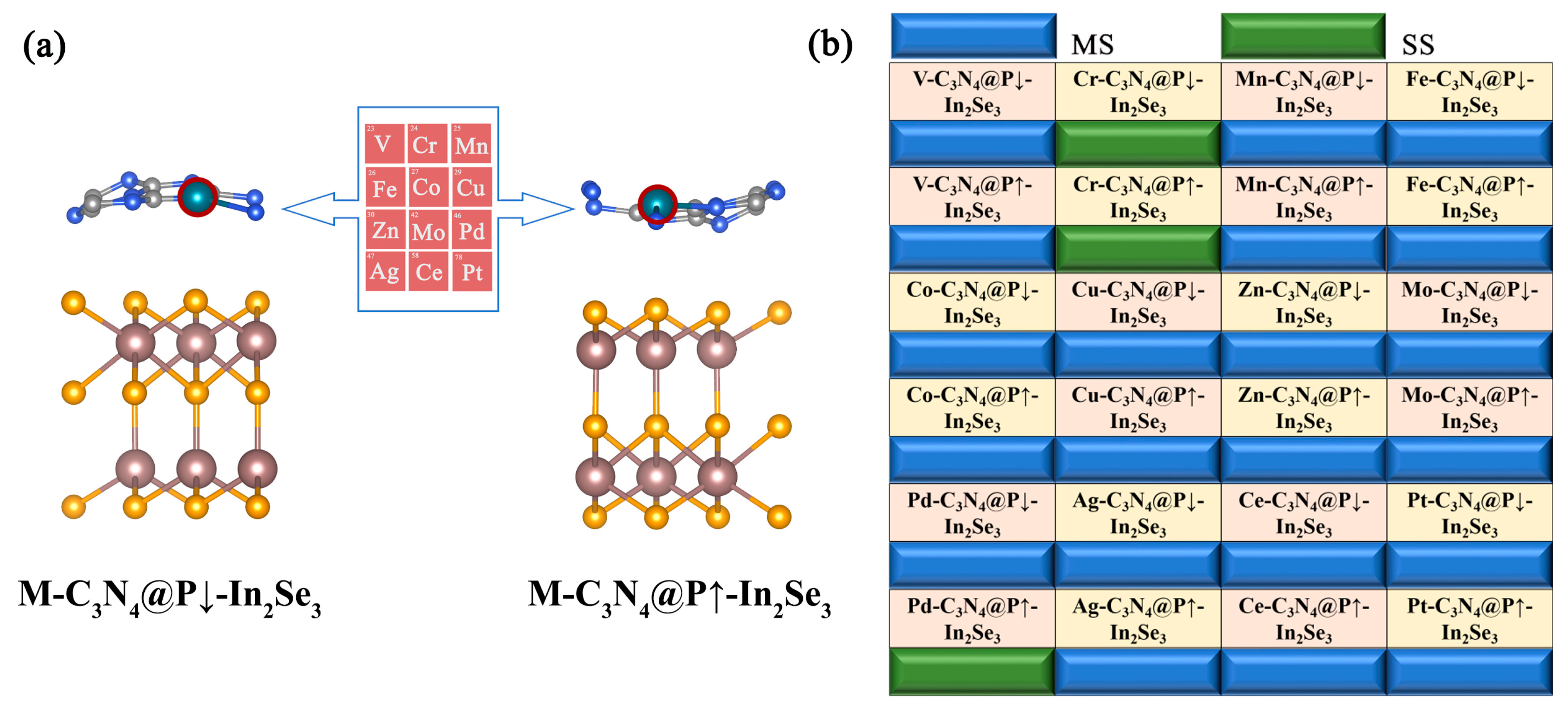
To enable a nonvolatile phase transition between semiconducting and metallic states during polarization reversal upon heterojunction formation with In2Se3, suitable metal dopants for g-C3N4 were systematically evaluated. The prior literature has established that transition metals such as Fe [38] and Co [39] effectively enhance oxygen evolution reaction (OER) activity and modulate electronic structures, while noble metals including Pd [40], Ag [41], and Pt [42] can be stably incorporated into the catalytic system to augment activity. Additionally, Mo doping has been shown to improve catalytic performance through the modulation of electronic structures and interfacial charge transfer [43]. Guided by these findings, twelve metal atoms, namely V, Cr, Mn, Fe, Co, Cu, Zn, Mo, Pd, Ag, Ce, and Pt, were preliminarily selected as doping candidates. These atoms were subsequently introduced into the C3N4 framework and combined with In2Se3 under P↓ and P↑ states to construct two heterostructural configurations, designated M-C3N4@P↓-In2Se3 and M-C3N4@P↑-In2Se3 (Figure 1a).
Based on the projected density of states (DOS) calculated via the Perdew–Burke–Ernzerhof (PBE) method for the M-C3N4@P↓-In2Se3 systems under both P↑ and P↓ polarization states (Figure 1b), a screening of suitable dopants was performed to identify those capable of inducing an electronic phase transition upon reversal of the In2Se3 polarization. The DOS plots reveal that doping with V, Mn, Fe, Co, Cu, Zn, Mo, Ag, Ce, and Pt atoms imparts metallic character to the M-C3N4@P↓-In2Se3 heterostructures in both spin channels (Figure S1a,c,d,f–h,j–l). In contrast, Cr doping results in semiconducting behavior in both spin channels (Figure S1b). Notably, Pd doping is found to enable an electronic phase transition in the heterostructure when the polarization orientation of In2Se3 is reversed. Specifically, as illustrated in Figure S1i, the Pd-C3N4@P↑-In2Se3 configuration exhibits semiconducting character, whereas the Pd-C3N4@P↓-In2Se3 configuration shows metallic behavior.

2.2. Structural and Electronic Properties of the Pd-C3N4@In2Se3 Heterojunction

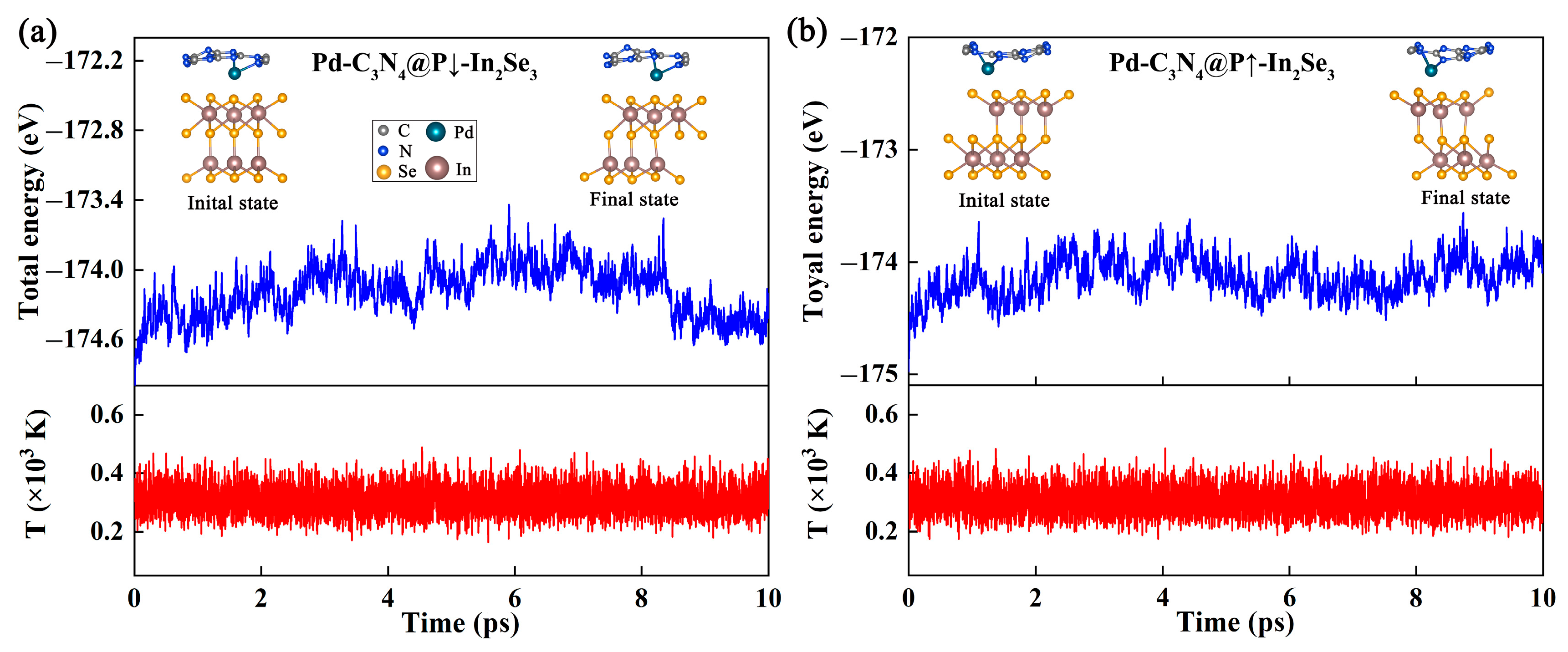
As shown in Figure S2, the interlayer distances of Pd-C3N4@P↑-In2Se3 and Pd-C3N4@P↓-In2Se3 are 3.41 Å and 3.39 Å, respectively, indicating that the heterojunction layers are primarily bonded by van der Waals forces. The formation energies of Pd-C3N4@P↑-In2Se3 and Pd-C3N4@P↓-In2Se3 were derived from Equation (1) as −0.044 eV/Å2 and −0.083 eV/Å2, respectively. These negative values confirm the energetic favorability of the ferroelectric heterojunction. In addition, the ab initio molecular dynamics (AIMD) simulations (Figure 2a,b) reveal that the structures remain intact and the total energy converges toward a stable plateau, further attesting to the excellent thermodynamic stability of the Pd-C3N4@In2Se3 heterojunction.
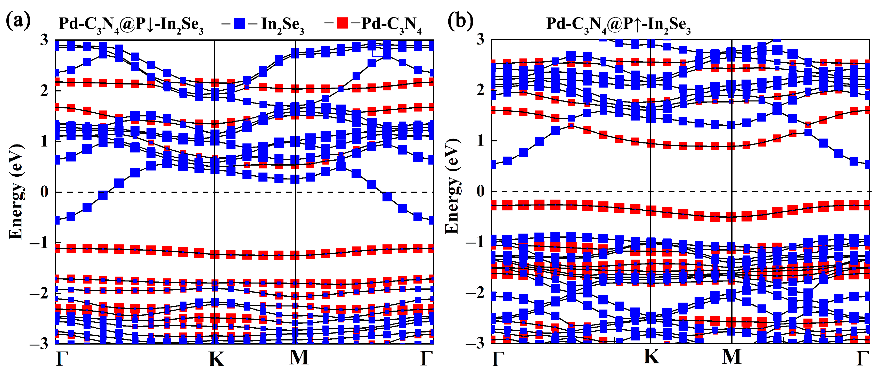
As mentioned before, the DOS results at PBE state that the Pd-C3N4@In2Se3 heterostructure undergoes an electronic phase transition upon the reversal of the polarization orientation of In2Se3. As displayed in Figure 3, the HSE06 results of the electronic band structures further confirm this point. When the polarization state of In2Se3 switches to the P↓ state, the heterojunction exhibits MS, with the conduction band of In2Se3 component crossing the Fermi level (Figure 3a). When the polarization state of In2Se3 switches to the P↑ state, the heterojunction becomes SS (Figure 3b). In this case, the CBM of In2Se3 component is lower than that of Pd-C3N4 component but higher than the VBM of Pd-C3N4 component, whereas the VBM of In2Se3 component is lower than that of Pd-C3N4 component, indicating that, the Pd-C3N4@P↑-In2Se3 heterojunction has a typical type-II band alignment structure. The band offsets for CBM and VBM are 0.37 eV and 0.64 eV, respectively.
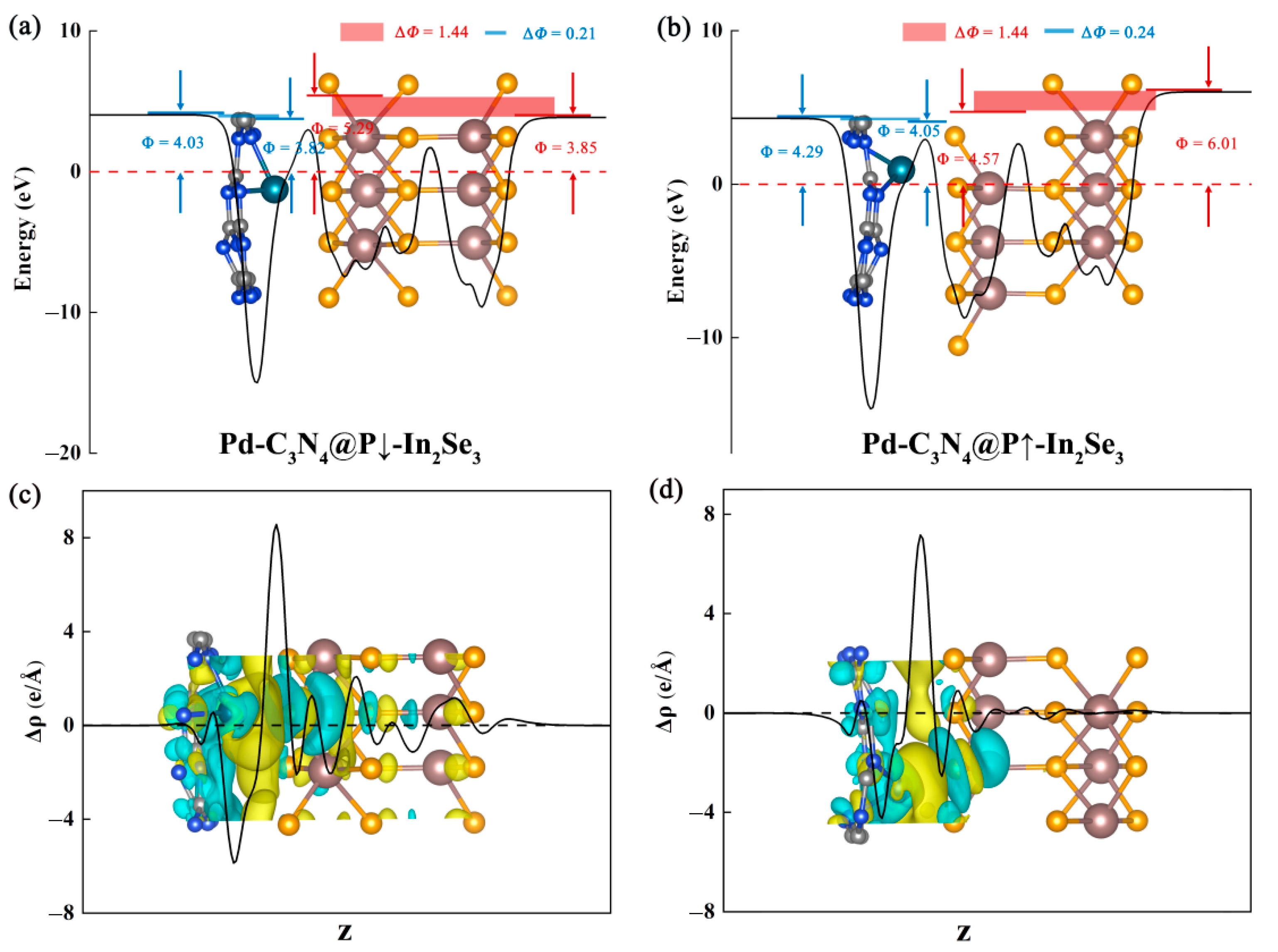
The physical origin of the MS-SS phase transition can be attributed to the reversal of the interfacial built-in electric field direction and the difference in the interfacial electron transfer, induced by the polarization reversal of the α-In2Se3 ferroelectric layer. The symmetry breaking in In2Se3 layer leads to differences in the in-plane averaged electrostatic potentials on the opposite sides. The work function of the top surface is 5.21 eV, while that of the bottom surface is 6.65 eV (Figure S3); therefore, the potential difference (∆Φ) for the In2Se3 layer is 1.44 eV. As to the case of Pd-C3N4 layer, as shown in Figure S4, due to its asymmetric structure, the work functions of its top and bottom surfaces are not equal. Given the configurational variation in Pd-C3N4 layer between the Pd-C3N4@P↓-In2Se3 and Pd-C3N4@P↑-In2Se3 heterostructures, the resulting potential differences are disparate. Therefore, when determining the potential difference at the interfaces of Pd-C3N4@P↓-In2Se3 and Pd-C3N4@P↑-In2Se3 heterostructures, the potential difference derived from the configuration of Pd-C3N4 layer in the relevant heterostructure was taken as the reference benchmark (Figure S4a,b).
As shown in Figures S3 and S4, before the formation of the Pd-C3N4@P↓-In2Se3 heterostructure, the work function on the Pd-C3N4 side (3.88 eV) is 2.77 eV lower than that on the In2Se3 side (6.65 eV). This work-function difference provides the driving force for electron transfer from the Pd-C3N4 side to the In2Se3 side during the mutual contact for the formation of the Pd-C3N4@P↓-In2Se3 heterostructure. For the case of the Pd-C3N4@P↑-In2Se3 heterostructure, the work function on the Pd-C3N4 side (3.99 eV) is also lower than that on the In2Se3 side (5.21 eV), but by only 1.22 eV. Since the work-function difference between the Pd-C3N4 side and the In2Se3 side in the Pd-C3N4@P↑-In2Se3 heterostructure is smaller than that in the Pd-C3N4@P↓-In2Se3 heterostructure, the driving effect for electron transfer from the Pd-C3N4 side to the In2Se3 side at the interface of the Pd-C3N4@P↓-In2Se3 heterostructure is greater than that at the interface of the Pd-C3N4@P↑-In2Se3 heterostructure. This is confirmed by charge density difference analysis, which shows more pronounced electron transfer at the Pd-C3N4@P↓-In2Se3 interface (as shown in Figure 4c,d). Moreover, the Bader charge analysis also states that the number of transferred electrons in Pd-C3N4@P↓-In2Se3 interface is larger than that in the Pd-C3N4@P↑-In2Se3 interface by 0.11 e.
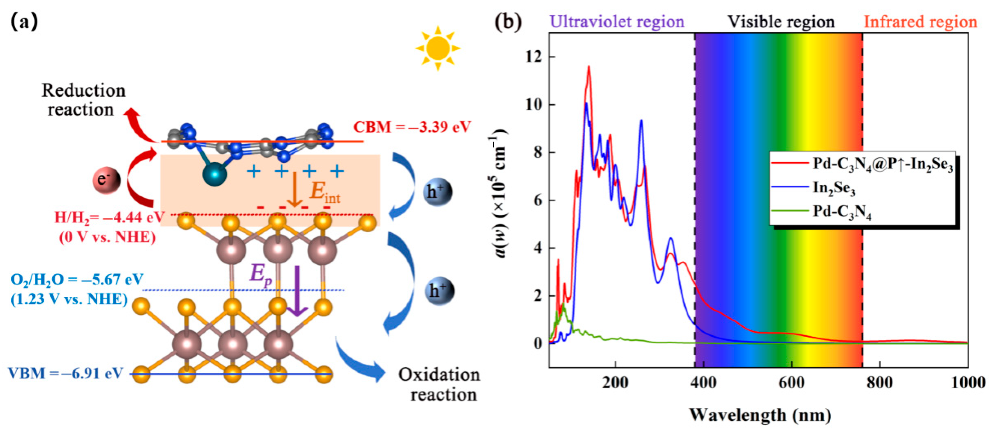
In the semiconducting phase of Pd-C3N4@P↑-In2Se3 heterostructure, a built-in electric field (Eint) oriented from Pd-C3N4 region to In2Se3 region is established at the interface, arising from the work-function-difference-driven charge transfer during the contact process. As shown in Figure 4b, upon formation of the Pd-C3N4@P↑-In2Se3 heterostructure, the work-function difference at the interface is reduced to 0.52 eV owing to the built-in electric field. The strength of the built-in electric field could be characterized by the change in the work-function difference at the interface (0.70 eV). Under light illumination, the flow of photogenerated carriers at the interface of the Pd-C3N4@P↑-In2Se3 heterostructure is simultaneously affected by both the band offset and the built-in electric field, and these two effects act in opposite directions. As shown in Figure 3b, the band offset causes photoelectrons and photogenerated holes to accumulate on the In2Se3 and the Pd-C3N4 sides, respectively. However, the built-in electric field at the interface drives photoelectrons and photogenerated holes to accumulate on the Pd-C3N4 and the In2Se3 sides, respectively. Since the driving voltage provided by the built-in electric field (0.7 V) is larger than that provided by the band offset (0.37 V for electrons and 0.64 V for holes), the migration trajectory of photogenerated carriers is dominated by the effect of the built-in electric field. As shown in Figure 5a, upon photoexcitation, the photogenerated electrons at the interface are driven toward the Pd-C3N4 layer, whereas the photogenerated holes are correspondingly driven toward In2Se3 layer, and arrive at its surface with the help of the intrinsic built-in electric field (Ep) in the In2Se3 regions. As a consequence, the Pd-C3N4 layer enriched with photogenerated electrons can serve as an active site for the HER, while the In2Se3 layer enriched with photogenerated holes acts as an active site for the OER. The band-edge potentials of Pd-C3N4@P↑-In2Se3 heterojunction were also evaluated to determine whether it exhibits adequate redox strength to enable overall water splitting. The band-edge potentials presented in Figure 5a reveal that the CBM of the Pd-C3N4 moiety lies at −3.39 eV (vs. vacuum), which is more positive than the H+/H2 reduction potential. In contrast, the VBM of the In2Se3 moiety lies at −6.91 eV (vs. vacuum), which is more negative than the H2O/O2 oxidation potential. On the basis of these thermodynamic criteria, the Pd-C3N4 component is identified as the HER-active photocatalyst with sufficient reduction capacity to transform H+ into H2, while the In2Se3 component functions as the OER-active counterpart meeting the energy requirement for efficient oxidation of water molecules to O2. Accordingly, the two sides of Pd-C3N4@P↑-In2Se3 heterostructure are favorable for the HER and OER, respectively, thereby providing a promising catalytic interface for achieving efficient overall water splitting.
As shown in Figure 5b, the Pd-C3N4@P↑-In2Se3 heterostructure exhibits a pronounced light absorption coefficient peak of 1.20 × 106 cm−1 at 140.26 nm, substantially higher than that of pristine In2Se3 (9.99 × 105 cm−1 at 131.03 nm, blue line) and Pd-C3N4 (1.65 × 105 cm−1 at 82.08 nm, green line) monolayers. Moreover, the initial optical absorption peak of Pd-C3N4@P↑-In2Se3 heterostructure redshifts significantly, relative to the ones from both component materials. The significant increase in both the maximum absorption peak intensity and the optical absorption spectral range, observed for Pd-C3N4@P↑-In2Se3 heterojunction compared with its constituent materials, indicates that the heterojunction configuration contributes to an enhanced light-harvesting capacity and improved photocatalytic performance.
In order to further verify this point, we calculate the light absorption efficiency (ηabs), carrier utilization efficiency (ηcu), STH efficiency (ηSTH), and the corrected solar-to-hydrogen efficiency (η′STH) of the Pd-C3N4 monolayer, In2Se3 monolayer, and Pd-C3N4@P↑-In2Se3 heterostructure with the previous method [44], using their band gaps, over-potential for hydrogen evolution reaction (χ(H2)) and oxygen evolution reaction (χ(O2)), and ΔΦ, which have been listed in Table S1. An enhancement in the light absorption efficiency ηabs is observed for the heterostructure design in Table S2, attributable to the reduced band gap, which aligns well with the foregoing absorption analyses. Specifically, the ηabs of Pd-C3N4@P↑-In2Se3 heterostructure is 13.68% higher than that of Pd-C3N4 component and 28.53% higher than that of In2Se3 component. Since Pd-C3N4 component does not possess sufficient oxidation ability to oxidize H2O into O2 (χ(O2) < 0, as listed Table S1), its ηcu and ηSTH are not considered here. Compared with the In2Se3 component, the heterostructure configuration further increases ηcu, as the substantial ΔΦ markedly boosts the reduction potential of the photogenerated electrons. Consequently, the ηSTH of the Pd-C3N4@P↑-In2Se3 heterostructure attains 65.46%, far surpassing that of the bare In2Se3 component (35.65%). After accounting for the ΔΦ effect, the η′STH of this heterostructure still reaches 34.18%, which exceeds the commercial viability threshold (>10%) [45].

2.3. Adsorption of Water Molecules

The strength of H2O adsorption is widely regarded as a critical descriptor for evaluating the catalytic activity of HER catalysts [46,47]. In this work, the semiconducting phase of material Pd-C3N4@In2Se3 (Pd-C3N4@P↑-In2Se3), which exhibits relatively poor electrical conductivity, was chosen to assess its hydrophilicity according to the adsorption energy (Eads) for water molecules.
We separately studied the adsorption behavior of H2O molecules at the surfaces of the Pd-C3N4 and In2Se3 components. The Eads was defined using the following equation:
E ads =   E total − E Pd- C 3 N 4 @ P ↑ - In 2 Se 3 −   E H 2 O
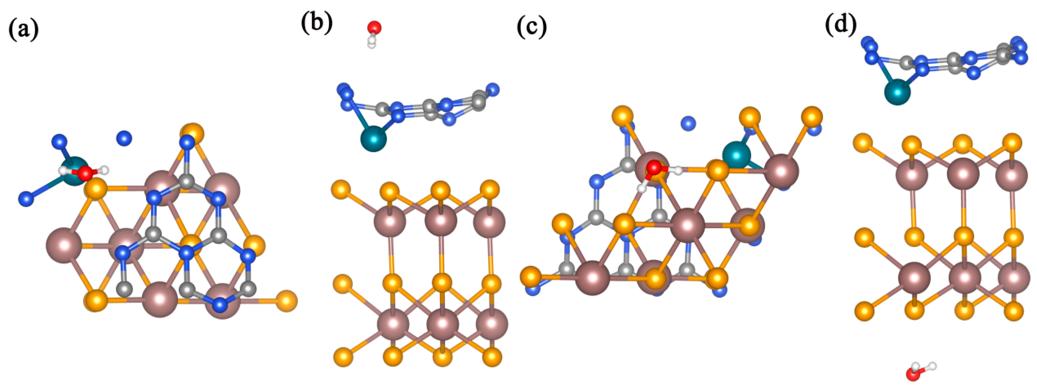
where Etotal is the total energy of the whole H2O adsorption system, E Pd- C 3 N 4 @ P ↑ - In 2 Se 3 is the energy of the pristine Pd-C3N4@P↑-In2Se3 heterostructure, and   E H 2 O is the energy of an isolated H2O molecule. For the Pd-C3N4 layer, the most energetically favorable configuration corresponds to the O atom of H2O binding to the N site adjacent to the Pd atom, yielding the Eads of −0.21 eV. For the surface of the ferroelectric In2Se3 layer, various possible adsorption sites were systematically evaluated via geometric optimization (Figure S5) to determine the most stable configuration. As listed in Table S3, the calculated Eads values for H2O on the In, Se1, and Se2 sites are −0.16, −0.19, and −0.11 eV, respectively, establishing Se1 as the most favorable adsorption site on the In2Se3 surface (Figure 6). Collectively, these results demonstrate that H2O molecules can be stably co-adsorbed on both the upper and lower surfaces of the Pd-C3N4@P↑-In2Se3 heterostructure. Such dual-surface adsorption behavior ensures an adequate supply of reactant molecules for the subsequent catalytic reactions.

2.4. The HER on Pd-C3N4@In2Se3

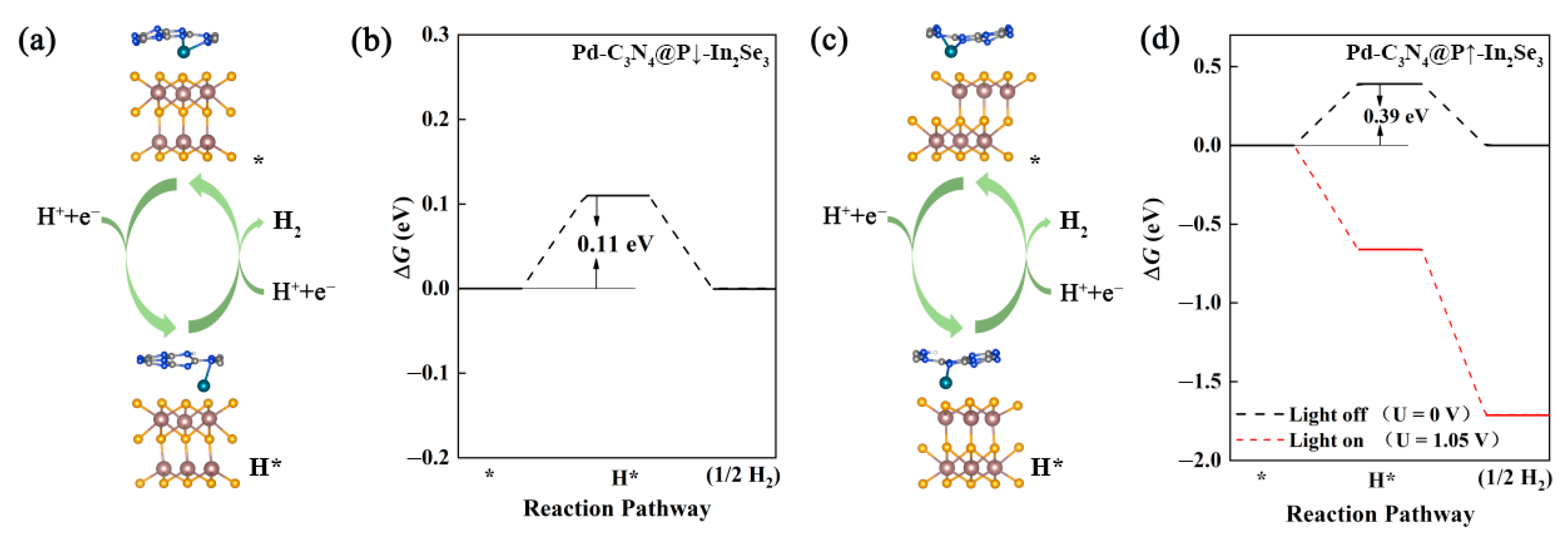
The metallic-state Pd-C3N4@P↓-In2Se3 can serve as an HER electrocatalyst (Figure 7a), where the N sites in Pd-C3N4 act as the active sites for HER (Figure S6), exhibiting a limiting potential of only −0.11 V (Figure 7b), and the formation of H* is the rate-determining step. We also examined H adsorption on the embedded single Pd atom site. Interestingly, upon full structural relaxation, the H atom initially placed on the Pd site spontaneously migrated to the adjacent N site in both the P↓ and P↑ polarization states, indicating that the N site is energetically more favorable for H* adsorption than the Pd site, regardless of the polarization direction. This confirms that the N sites, rather than the Pd atoms, serve as the primary active centers for HER in the metallic Pd-C3N4@P↓-In2Se3 state, while in the semiconducting P↑ state, the N sites remain the active sites for photocatalytic HER. Meanwhile, for the photocatalytic HER performance on the semiconducting Pd-C3N4@P↑-In2Se3, the ΔGH* is 0.39 eV according to the Gibbs free energy calculations at pH = 0 (Figure 7d). This is superior to many theoretically predicted HER photocatalysts, such as the Janus WSSe monolayer (ΔGH* = 0.41 eV) [46] and the PdSeO3 monolayer (ΔGH* = 0.57 eV) [48]. Under an external potential provided by photogenerated electrons of Ue = 1.05 V, both hydrogenation steps of the HER on the Pd-C3N4@P↑-In2Se3 heterojunction are downhill (Figure 7d). This indicates that the driving potential provided by the photogenerated electrons enables the complete reaction pathway of the HER to proceed spontaneously.
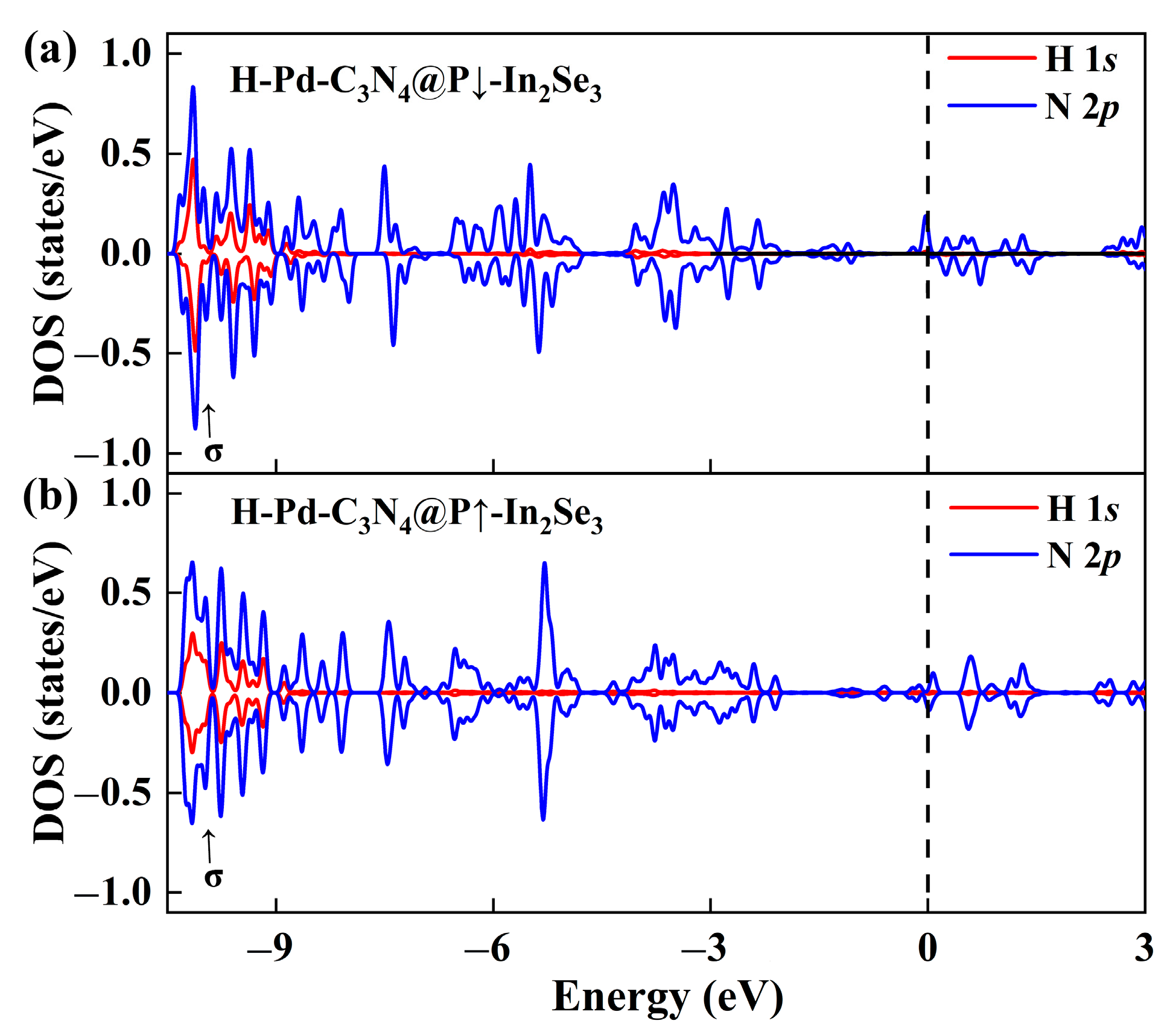
Our computational results reveal that the metallic Pd-C3N4@P↓-In2Se3 surface delivers a substantially lower HER limiting potential (−0.11 V) than its upward-polarized counterpart (Pd-C3N4@P↑-In2Se3). To elucidate the electronic origin of this performance difference, we systematically investigated the effect of polarization direction on H* adsorption. As shown in Figure 8a,b, the N 2p orbitals in the σ-bonding region of the downward-polarized configuration exhibit markedly enhanced delocalization relative to the upward-polarized case. This enhanced delocalization promotes more pronounced orbital overlap between the N 2p and H 1s states, which strengthens H* adsorption, leading to significant improvement in HER activity.

2.5. The Photocatalytic OER on Pd-C3N4@P↑-In2Se3

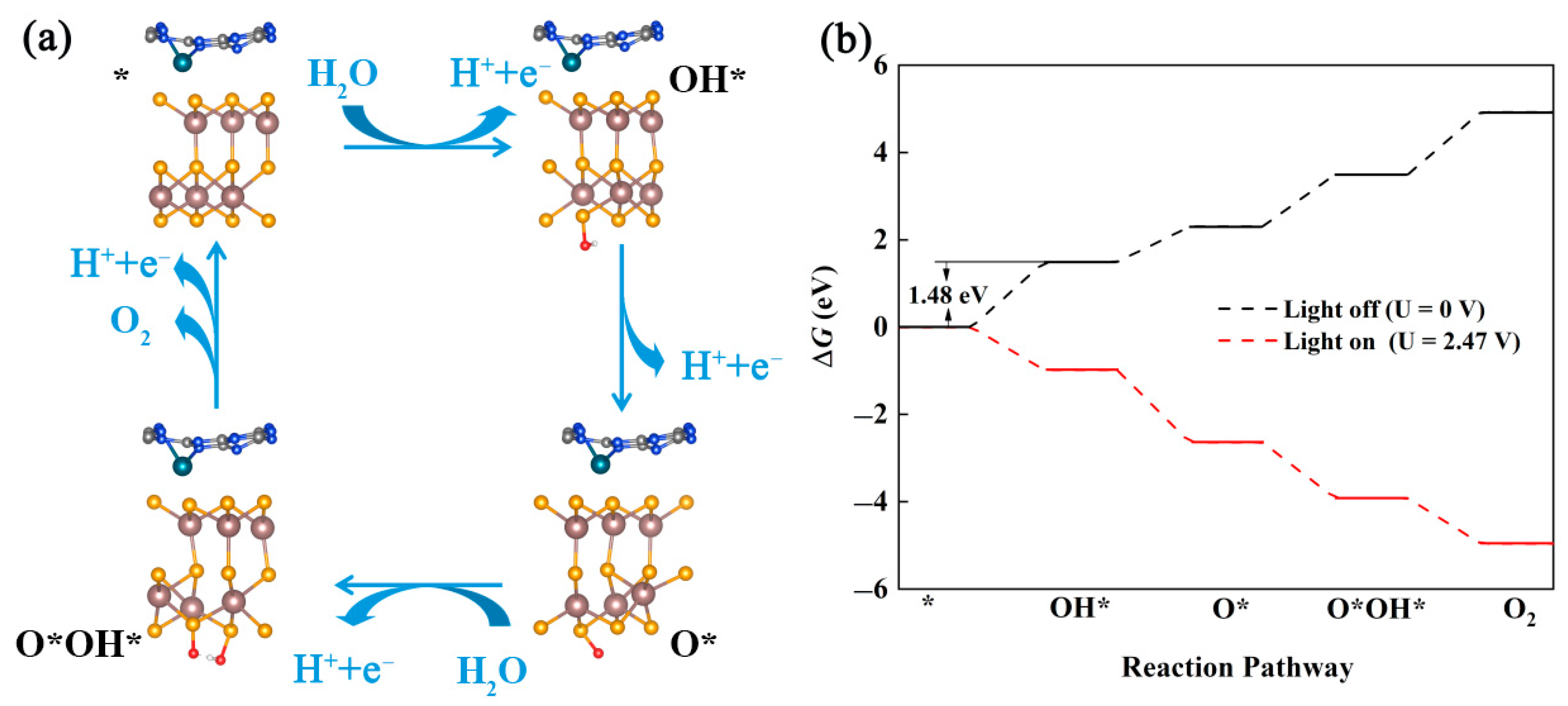
To consume accumulated photogenerated holes and produce H+ for the HER, this study further considers the OER on the bottom surface of the In2Se3 component in Pd-C3N4@P↑-In2Se3. Specifically, the OER at this site follows a classical four-electron pathway involving four proton-coupled electron transfer steps. As shown in Figure S7, based on the calculations of the free energies of the reaction intermediates, we screened out the optimal OER pathway from the two reaction pathways. The selected OER pathway could be expressed as: * + H2O → OH* + H+ + e−, OH* → O* + H+ + e−, O* + H2O → O*OH* + H+ + e−, O*OH* → * + O2(g) + H+ + e−, with OH, O, and O*OH* as intermediates (Figure 9a). Under dark conditions at pH = 0, the limiting potential corresponding to the maximum thermodynamic barrier that needs to be overcome to complete this OER is calculated to be 1.48 V (Figure 9b). And the first hydrogenation step (* + H2O → OH* + H+ + e−) is the rate-determining step. However, under illumination, when the external potential (Uh = 2.47 V) is provided by photogenerated holes, the rate-determining step becomes a downhill reaction (Figure 9b), indicating that this reaction can proceed spontaneously under illumination.

3. Computational Details

All calculations were carried out using spin-polarized density functional theory (DFT) simulations as implemented in the Vienna Ab initio Simulation Program (VASP) code [49,50]. Exchange-correlation effects were treated with the spin-polarized generalized gradient approximation (GGA) in the PBE parametrization, while electron–ion interactions were described via the frozen-core projector augmented wave (PAW) method [51,52,53]. Van der Waals (vdW) forces were accounted for through Grimme’s DFT-D3 dispersion correction scheme [54]. To construct the metal-doped C3N4 (M-C3N4) model, a single metal atom was placed at the center of the N-ring in a 1 × 1 C3N4 supercell. The Pd-C3N4@In2Se3 heterostructure was built by vertically stacking a 3 × 3 In2Se3 layer (lattice constants a = b = 7.05 Å) onto a 1 × 1 Pd-C3N4 layer (lattice constants a = b = 7.14 Å). Given that the polarization state of In2Se3 layer depends sensitively on the lattice constant [55], the lattice constant of In2Se3 layer is chosen for the construction of Pd-C3N4@In2Se3 heterostructure. Under this configuration, the lattice mismatch of Pd-C3N4 layer is merely 1.26% along both X and Y axes (Table S6). A vacuum spacing exceeding 30 Å was introduced along the out-of-plane direction to eliminate interactions between periodic images, and dipole corrections were applied to all asymmetric structures [56]. Brillouin-zone integration employed a 3 × 3 × 1 Monkhorst-Pack k-mesh for the two-dimensional system. Site-specific charge populations were derived from Bader analysis. To remedy the band-gap underestimation typical of PBE, the electronic structure was further evaluated with the Heyd–Scuseria–Ernzerhof (HSE06) hybrid functional [57]. The plane-wave cutoff energy was set to 500 eV, and convergence criteria for forces and total energy were 10−2 eV/Å and 10−5 eV, respectively. Gibbs free energies were obtained using the computational hydrogen electrode (CHE) model [58]. For the free-energy calculations of HER and OER, solvent effects were accounted for by the implicit solvation model implemented in the VASPsol software (version VASP 6.4.1) [47,59], with a relative dielectric constant of 80.0 for water. Additional simulation details can be found in the Supporting Information.
Formation energy (Ef) is a fundamental metric to assess the stability of materials, and it has been calculated as:
E f = ( E Pd- C 3 N 4 @ In 2 Se 3 − E Pd- C 3 N 4 − E In 2 Se 3 ) / S
where E Pd- C 3 N 4 @ In 2 Se 3 represents the total energy of the Pd-C3N4@In2Se3 heterostructure, E Pd- C 3 N 4 is the energy of Pd-C3N4 monolayer, E In 2 Se 3 is the energy of In2Se3 monolayer, and S denotes the interfacial area of the Pd-C3N4@In2Se3 heterostructures.
The charge density difference for the Pd-C3N4@In2Se3 ( ∆ ρ * ) is calculated by the following equation:
∆ ρ * = ρ Pd- C 3 N 4 @ In 2 Se 3 − ρ Pd- C 3 N 4 − ρ In 2 Se 3
where ρ Pd- C 3 N 4 @ In 2 Se 3 is the charge density of the Pd-C3N4@In2Se3 heterostructures. ρ Pd- C 3 N 4 and ρ In 2 Se 3 are the charge densities of the Pd-C3N4 and In2Se3 monolayers, respectively.
To extract the orbital-resolved components, we used the “splittos.dos” code to analyze the DOS output file. The average d-band center shifts in the surface metal atoms were computed from both the total and orbital-resolved d partial densities of states. The d-band center (Ed) was then evaluated using the following expression [60]:
E d = ∫ n d ( E ) Eds ∫ n d ( E ) ds
where E is the electronic energy of states, and n d ( E ) is the electronic density of states.
The light-harvesting capability was evaluated by the absorption coefficient α(ω), which was computed using the following formula [61]:
α ( ω ) = 2 ω c ( ε 1 ( ω ) 2 + ε 2 ( ω 2 ) − ε 1 ( ω ) ) 1 2
where the real and imaginary components of a frequency-dependent dielectric function are denoted by ε1 and ε2, respectively, while the vacuum speed of light is denoted by c.

4. Conclusions

Our work systematically investigates the ferroelectric heterojunction Pd-C3N4@In2Se3 using first-principles DFT calculations. The electronic structure, optical absorption, and catalytic performance are examined under two opposite polarization states, namely P↑ and P↓. Reversing the polarization direction of the α-In2Se3 ferroelectric layer induces a nonvolatile electronic phase transition. The P↓ configuration exhibits metallic behavior, while the P↑ configuration becomes semiconducting with a typical type-II band alignment. This transition originates from the polarization-dependent interfacial built-in electric field and the consequent difference in charge transfer magnitude, as confirmed by work-function analysis and Bader charge quantification. In the semiconducting P↑ state, the heterojunction functions as an efficient photocatalyst, and its band edges straddle the water-redox potentials. Electrons accumulate on the Pd-C3N4 side for HER, and holes migrate to the In2Se3 side for OER. The Pd-C3N4@P↑-In2Se3 heterostructure shows a significantly enhanced optical absorption coefficient of 1.20 × 106 cm−1 at approximately 140 nm and a broadened spectral response compared to its constituents, confirming superior light-harvesting capability. Gibbs free energy calculations reveal that under illumination, both the HER with ΔGH* of 0.39 eV at pH = 0 and the OER with a limiting potential of 1.48 V become thermodynamically spontaneous when driven by photogenerated electrons (Ue = 1.05 V) and holes (Uh = 2.47 V), respectively. In contrast, the metallic P↓ state serves as an excellent electrocatalyst for HER, with a limiting potential as low as −0.11 V. More importantly, the present work provides an in-depth investigation into the microscopic mechanism of HER, revealing at the orbital level the intrinsic correlation between the ferroelectric polarization direction and the N 2p–H 1s hybridization strength, thereby further enriching the ferroelectric heterojunction catalytic system. Collectively, these results establish a feasible strategy to achieve on-demand switching between photocatalytic and electrocatalytic functions within a single heterostructure by simply tuning the ferroelectric polarization. This polarization-driven electronic phase transition not only resolves the conflicting electronic requirements of the two catalytic modes but also offers a new paradigm for designing smart, dual-functional catalysts that can adapt to varying energy inputs, such as sunlight or electricity. This work provides valuable theoretical guidance for experimental realization of switchable catalysis and paves the way toward more flexible and sustainable energy-conversion systems.

Supplementary Materials

The following supporting information can be downloaded at: https://www.mdpi.com/article/10.3390/catal16090756/s1, Figure S1: The DOS of the M-C3N4@In2Se3 monolayer; Figure S2: The optimized heterojunction structures of Pd-C3N4@In2Se3; Figure S3: The xy-plane average electrostatic potential of isolated In2Se3 monolayer; Figure S4: The xy-plane average electrostatic potential of Pd-C3N4; Figure S5: The adsorption site for H2O; Figure S6: The adsorption site for H; Figure S7: Gibbs free energy diagrams of OER along path 1 (OOH* path) and path 2; Table S1: The χ(H2), χ(O2), Eg, and ΔΦ; Table S2: The ηabs, ηcu, ηSTH, and η′STH; Table S3: The adsorption sites, Eads, and Etotal of H2O*; Table S4: The EZPE, TS, and Etotal of adsorbates on Pd-C3N4@P↓-In2Se3; Table S5: The EZPE, TS, and Etotal of adsorbates on Pd-C3N4@P↑-In2Se3; Table S6: The lattice constants and the lattice mismatch.

Author Contributions

Conceptualization, L.J.; Software, Y.Z.; Formal analysis, M.B., S.L. and L.J.; Investigation, S.X., M.B., S.C. and S.L.; Data curation, S.X. and Y.Z.; Writing—original draft, S.X., Y.Z., M.B., S.C. and L.J.; Writing—review and editing, S.L.; Visualization, Y.Z. and S.C.; Supervision, S.L. and L.J.; Project administration, L.J.; Funding acquisition, S.C. and L.J. All authors have read and agreed to the published version of the manuscript.

Funding

This work is funded by the National Natural Science Foundation of China (Grant No. 22573002), the Program for Science & Technology Innovation Talents in Universities of Henan Province (Grant No. 24HASTIT013), and the College Students Innovation Fund of Anyang Normal University (Grant No. 202610479046).

Institutional Review Board Statement

Not applicable.

Informed Consent Statement

Not applicable.

Data Availability Statement

The original contributions presented in this study are included in the article/Supplementary Materials. Further inquiries can be directed to the corresponding authors.

Acknowledgments

We thank the Computational Laboratory for Energy Conversion and Storage for the support.

Conflicts of Interest

The authors declare no conflicts of interest.

References

  1. Cho, H.; Seo, S.E.; Kwon, O.S.; Kim, H.-I. Photonic crystal-assisted sub-bandgap photocatalysis via triplet-triplet annihilation upconversion for the degradation of environmental organic pollutants. J. Hazard. Mater. 2024, 477, 135208. [Google Scholar] [CrossRef] [Scilit] [PubMed]
  2. Ju, L.; Ma, Y.; Tan, X.; Kou, L. Controllable electrocatalytic to photocatalytic conversion in ferroelectric heterostructures. J. Am. Chem. Soc. 2023, 145, 26393–26402. [Google Scholar] [CrossRef] [Scilit] [PubMed]
  3. Jin, X.; Ye, L.; Xie, H.; Chen, G. Bismuth-rich bismuth oxyhalides for environmental and energy photocatalysis. Coord. Chem. Rev. 2017, 349, 84–101. [Google Scholar] [CrossRef] [Scilit]
  4. Guo, X.; Du, H.; Qu, F.; Li, J. Recent progress in electrocatalytic nitrogen reduction. J. Mater. Chem. A 2019, 7, 3531–3543. [Google Scholar] [CrossRef] [Scilit]
  5. Li, L.; Tang, C.; Xia, B.; Jin, H.; Zheng, Y.; Qiao, S.-Z. Two-Dimensional Mosaic Bismuth Nanosheets for Highly Selective Ambient Electrocatalytic Nitrogen Reduction. ACS Catal. 2019, 9, 2902–2908. [Google Scholar] [CrossRef] [Scilit]
  6. Liu, X.; Li, Y.; Zhang, J.; Lu, J. Ultrathin Ni/V-layered double hydroxide nanosheets for efficient visible-light-driven photocatalytic nitrogen reduction to ammonia. Nano Res. 2021, 14, 3372–3378. [Google Scholar] [CrossRef] [Scilit]
  7. Huang, H.; Wang, X.-S.; Philo, D.; Ichihara, F.; Song, H.; Li, Y.; Li, D.; Qiu, T.; Wang, S.; Ye, J. Toward visible-light-assisted photocatalytic nitrogen fixation: A titanium metal organic framework with functionalized ligands. Appl. Catal. B Environ. 2020, 267, 118686. [Google Scholar] [CrossRef] [Scilit]
  8. Zhu, X.; Zhou, E.; Tai, X.; Zong, H.; Yi, J.; Yuan, Z.; Zhao, X.; Huang, P.; Xu, H.; Jiang, Z. g-C3N4 S-Scheme Homojunction through Van der Waals Interface Regulation by Intrinsic Polymerization Tailoring for Enhanced Photocatalytic H2 Evolution and CO2 Reduction. Angew. Chem. Int. Ed. 2025, 64, e202425439. [Google Scholar] [CrossRef] [Scilit] [PubMed]
  9. Wang, K.; Zhou, T.; He, J.; Cao, Z.; Jiang, Z. Regulating the atomic ratio of Pt/Ru to enhance CO anti-poisoning of Pt based electrocatalysts toward methanol oxidation reaction. Mol. Catal. 2024, 556, 113927. [Google Scholar] [CrossRef] [Scilit]
  10. Huang, Z.; Rafiq, M.; Woldu, A.R.; Tong, Q.-X.; Astruc, D.; Hu, L. Recent progress in electrocatalytic nitrogen reduction to ammonia (NRR). Coord. Chem. Rev. 2023, 478, 214981. [Google Scholar] [CrossRef] [Scilit]
  11. Yao, C.; Wang, R.; Wang, Z.; Lei, H.; Dong, X.; He, C. Highly dispersive and stable Fe3+ active sites on 2D graphitic carbon nitride nanosheets for efficient visible-light photocatalytic nitrogen fixation. J. Mater. Chem. A 2019, 7, 27547–27559. [Google Scholar] [CrossRef] [Scilit]
  12. Ju, L.; Bie, M.; Zhang, X.; Chen, X.; Kou, L. Two-dimensional Janus van der Waals heterojunctions: A review of recent research progresses. Front. Phys. 2021, 16, 13201. [Google Scholar] [CrossRef] [Scilit]
  13. Liu, S.; Wei, W.; Zhao, D.; Zhang, X.; Tang, Z.; Ju, L.; Kou, L. Polarization-Driven Control of Dynamically Tunable Solar-to-Hydrogen Conversion and On-Demand Water Splitting in 2D Janus-Ferroelectric Heterojunctions. Inorg. Chem. 2025, 64, 11119–11129. [Google Scholar] [CrossRef] [Scilit] [PubMed]
  14. Zhao, Y.; Zhang, J.J.; Yuan, S.; Chen, Z. Nonvolatile Electrical Control and Heterointerface-Induced Half-Metallicity of 2D Ferromagnets. Adv. Funct. Mater. 2019, 29, 1901420. [Google Scholar] [CrossRef] [Scilit]
  15. Liu, A.Y.; Cohen, M.L. Prediction of new low compressibility solids. Science 1989, 245, 841–842. [Google Scholar] [CrossRef] [Scilit] [PubMed]
  16. Zhu, D.; Zhou, Q. Nitrogen doped g-C3N4 with the extremely narrow band gap for excellent photocatalytic activities under visible light. Appl. Catal. B Environ. 2021, 281, 119474. [Google Scholar] [CrossRef] [Scilit]
  17. Bhanderi, D.; Lakhani, P.; Modi, C.K. Graphitic carbon nitride (gC3N4) as an emerging photocatalyst for sustainable environmental applications: A comprehensive review. RSC Sustain. 2024, 2, 265–287. [Google Scholar] [CrossRef] [Scilit]
  18. Yan, S.; Li, Z.; Zou, Z. Photodegradation of rhodamine B and methyl orange over boron-doped g-C3N4 under visible light irradiation. Langmuir 2010, 26, 3894–3901. [Google Scholar] [CrossRef] [Scilit] [PubMed]
  19. Galakhov, V.R.; Poteryaev, A.I.; Kurmaev, E.Z.; Anisimov, V.I.; Bartkowski, S.; Neumann, M.; Lu, Z.W.; Klein, B.M.; Zhao, T.-R. Valence-band spectra and electronic structure of CuFeO2. Phys. Rev. B 1997, 56, 4584–4591. [Google Scholar] [CrossRef] [Scilit]
  20. Wang, Y.; Di, Y.; Antonietti, M.; Li, H.; Chen, X.; Wang, X. Excellent visible-light photocatalysis of fluorinated polymeric carbon nitride solids. Chem. Mater. 2010, 22, 5119–5121. [Google Scholar] [CrossRef] [Scilit]
  21. Wang, X.; Maeda, K.; Chen, X.; Takanabe, K.; Domen, K.; Hou, Y.; Fu, X.; Antonietti, M. Polymer Semiconductors for Artificial Photosynthesis: Hydrogen Evolution by Mesoporous Graphitic Carbon Nitride with Visible Light. J. Am. Chem. Soc. 2009, 131, 1680–1681. [Google Scholar] [CrossRef] [Scilit] [PubMed]
  22. Di, Y.; Wang, X.; Thomas, A.; Antonietti, M. Making Metal-Carbon Nitride Heterojunctions for Improved Photocatalytic Hydrogen Evolution with Visible Light. ChemCatChem 2010, 2, 834–838. [Google Scholar] [CrossRef] [Scilit]
  23. Yang, Y.; Guo, Y.; Liu, F.; Yuan, X.; Guo, Y.; Zhang, S.; Guo, W.; Huo, M. Preparation and enhanced visible-light photocatalytic activity of silver deposited graphitic carbon nitride plasmonic photocatalyst. Appl. Catal. B Environ. 2013, 142, 828–837. [Google Scholar] [CrossRef] [Scilit]
  24. Huang, L.; Xu, H.; Li, Y.; Li, H.; Cheng, X.; Xia, J.; Xu, Y.; Cai, G. Visible-light-induced WO3/gC3N4 composites with enhanced photocatalytic activity. Dalton Trans. 2013, 42, 8606–8616. [Google Scholar] [CrossRef] [Scilit] [PubMed]
  25. Zhou, X.; Jin, B.; Chen, R.; Peng, F.; Fang, Y. Synthesis of porous Fe3O4/g-C3N4 nanospheres as highly efficient and recyclable photocatalysts. Mater. Res. Bull. 2013, 48, 1447–1452. [Google Scholar] [CrossRef] [Scilit]
  26. Liu, B.; Bie, C.; Zhang, Y.; Wang, L.; Li, Y.; Yu, J. Hierarchically porous ZnO/g-C3N4 S-scheme heterojunction photocatalyst for efficient H2O2 production. Langmuir 2021, 37, 14114–14124. [Google Scholar] [CrossRef] [Scilit] [PubMed]
  27. Mehtab, A.; Mao, Y.; Alshehri, S.M.; Ahmad, T. Photo/electrocatalytic hydrogen evolution using Type-II Cu2O/g-C3N4 Heterostructure: Density functional theory addresses the improved charge transport efficiency. J. Colloid Interf. Sci. 2023, 652, 1467–1480. [Google Scholar] [CrossRef] [Scilit] [PubMed]
  28. Li, Q.; Zong, L.; Xing, Y.; Wang, X.; Yu, L.; Yang, J. Preparation of g-C3N4/TiO2 nanocomposites and investigation of their photocatalytic activity. Sci. Adv. Mater. 2013, 5, 1316–1322. [Google Scholar] [CrossRef] [Scilit]
  29. Li, Y.; Huang, L.; Xu, J.; Xu, H.; Xu, Y.; Xia, J.; Li, H. Visible-light-induced blue MoO3–C3N4 composite with enhanced photocatalytic activity. Mater. Res. Bull. 2015, 70, 500–505. [Google Scholar] [CrossRef] [Scilit]
  30. Liu, X.; Cheng, P.; Zhang, X.; Shen, T.; Liu, J.; Ren, J.-C.; Wang, H.; Li, S.; Liu, W. Enhanced solar-to-hydrogen efficiency for photocatalytic water splitting based on a polarized heterostructure: The role of intrinsic dipoles in heterostructures. J. Mater. Chem. A 2021, 9, 14515–14523. [Google Scholar] [CrossRef] [Scilit]
  31. Rahimi, K.; Moshfegh, A.Z. Interfacial control at Janus WSSe/Triazine g-C3N4 heterostructures in developing type-II and Z-scheme photocatalysts. J. Phys. Chem. C 2023, 127, 16792–16801. [Google Scholar] [CrossRef] [Scilit]
  32. Li, J.; Lin, Y.; Zhang, M.; Peng, Y.; Wei, X.; Wang, Z.; Jiang, Z.; Du, A. Ferroelectric polarization and interface engineering coupling of Z-scheme ZnIn2S4/α-In2Se3 heterostructure for efficient photocatalytic water splitting. J. Appl. Phys. 2023, 133, 105702. [Google Scholar] [CrossRef] [Scilit]
  33. Liu, X.; Wang, J.; Ling, F.; Shen, L. Mechanical control of photocatalysis in 2D ferroelectrics. Sol. RRL 2023, 7, 2300589. [Google Scholar] [CrossRef] [Scilit]
  34. Zhao, P.; Ma, Y.; Lv, X.; Li, M.; Huang, B.; Dai, Y. Two-dimensional III2-VI3 materials: Promising photocatalysts for overall water splitting under infrared light spectrum. Nano Energy 2018, 51, 533–538. [Google Scholar] [CrossRef] [Scilit]
  35. Zhou, Y.; Wu, D.; Zhu, Y.; Cho, Y.; He, Q.; Yang, X.; Herrera, K.; Chu, Z.; Han, Y.; Downer, M.C.; et al. Out-of-Plane Piezoelectricity and Ferroelectricity in Layered alpha-In2Se3 Nanoflakes. Nano Lett. 2017, 17, 5508–5513. [Google Scholar] [CrossRef] [Scilit] [PubMed]
  36. Cui, C.; Hu, W.J.; Yan, X.; Addiego, C.; Gao, W.; Wang, Y.; Wang, Z.; Li, L.; Cheng, Y.; Li, P.; et al. Intercorrelated In-Plane and Out-of-Plane Ferroelectricity in Ultrathin Two-Dimensional Layered Semiconductor In2Se3. Nano Lett. 2018, 18, 1253–1258. [Google Scholar] [CrossRef] [Scilit] [PubMed]
  37. Ju, L.; Tan, X.; Mao, X.; Gu, Y.; Smith, S.; Du, A.; Chen, Z.; Chen, C.; Kou, L. Controllable CO2 electrocatalytic reduction via ferroelectric switching on single atom anchored In2Se3 monolayer. Nat. Commun. 2021, 12, 5128. [Google Scholar] [CrossRef] [Scilit] [PubMed]
  38. Li, Z.; Xu, C.; Zhang, Z.; Xia, S.; Li, D.; Liu, L.; Chen, P.; Dong, X. Reversing the Interfacial Electric Field in Metal Phosphide Heterojunction by Fe-Doping for Large-Current Oxygen Evolution Reaction. Adv. Sci. 2024, 11, 2308477. [Google Scholar] [CrossRef] [Scilit] [PubMed]
  39. Chen, X.; Jin, W.; Zhong, X.; Lin, H.; Ding, J.; Liu, X.; Wang, H.; Chen, F.; Xiong, Y.; Ding, C. Optimized kinetic pathways of active hydrogen generation at Cu2O/Cu heterojunction interfaces to enhance nitrate electroreduction to ammonia. Chin. J. Catal. 2025, 79, 78–90. [Google Scholar] [CrossRef] [Scilit]
  40. Hu, W.-Y.; Li, Q.-Y.; Xu, D.; Gao, P.; Qiao, P.-Z.; Li, D.; Xia, S.-Y.; Lin, X.; Chen, J.-S.; Li, X.-H. Integrating Pd (I) atoms in schottky junctions for visible-light-driven urea production from ambient nitrogenous species and CO2. CCS Chem. 2024, 6, 3008–3017. [Google Scholar] [CrossRef] [Scilit]
  41. Wei, D.; Dong, H.; Ouyang, B.; Chen, P.; Zhang, T.; Wu, B.; He, Y.; Huang, L.; Wang, H. Constructing built-in electric field in Ag/Co7Fe3 heterostructures for improved electrochemical deionization performance. Chem. Eng. J. 2025, 516, 164154. [Google Scholar] [CrossRef] [Scilit]
  42. Sun, H.; Guo, Y.; Yu, X.; Tian, Y.; Gao, F.; Wang, B.; Tang, Y.; Assi, D.S.; Roy, V.A.L. Single-Atom Pt Anchoring on Self-Doped ZrO2@G-C3N4 Nanostructure Enables Efficient Photocatalytic Seawater Hydrogen Evolution. Adv. Sci. 2026, 13, e19332. [Google Scholar] [CrossRef] [Scilit] [PubMed]
  43. Zhang, R.; Qian, B.; Zhang, D.; Chen, C.; Luo, Y.; Xu, K.; Said, A.; Jiang, J.; Chen, K.; Komarneni, S. Mo-Doping Emergence in FeOOH/NiSx Heterostructure for Ultrastable Alkaline Overall Water Electrolysis. ACS Catal. 2026, 16, 4631–4645. [Google Scholar] [CrossRef] [Scilit]
  44. Fu, C.F.; Sun, J.; Luo, Q.; Li, X.; Hu, W.; Yang, J. Intrinsic Electric Fields in Two-dimensional Materials Boost the Solar-to-Hydrogen Efficiency for Photocatalytic Water Splitting. Nano Lett. 2018, 18, 6312–6317. [Google Scholar] [CrossRef] [Scilit] [PubMed]
  45. Cox, C.R.; Lee, J.Z.; Nocera, D.G.; Buonassisi, T. Ten-percent solar-to-fuel conversion with nonprecious materials. Proc. Natl. Acad. Sci. USA 2014, 111, 14057–14061. [Google Scholar] [CrossRef] [Scilit] [PubMed]
  46. Ju, L.; Bie, M.; Tang, X.; Shang, J.; Kou, L. Janus WSSe Monolayer: An Excellent Photocatalyst for Overall Water Splitting. ACS Appl. Mater. Interfaces 2020, 12, 29335–29343. [Google Scholar] [CrossRef] [Scilit] [PubMed]
  47. Ju, L.; Shang, J.; Tang, X.; Kou, L. Tunable Photocatalytic Water Splitting by the Ferroelectric Switch in a 2D AgBiP2Se6 Monolayer. J. Am. Chem. Soc. 2020, 142, 1492–1500. [Google Scholar] [CrossRef] [Scilit] [PubMed]
  48. Qiao, M.; Liu, J.; Wang, Y.; Li, Y.; Chen, Z. PdSeO3 monolayer: Promising inorganic 2D photocatalyst for direct overall water splitting without using sacrificial reagents and cocatalysts. J. Am. Chem. Soc. 2018, 140, 12256–12262. [Google Scholar] [CrossRef] [Scilit] [PubMed]
  49. Kresse, G.; Furthmüller, J. Efficient iterative schemes for ab initio total-energy calculations using a plane-wave basis set. Phys. Rev. B 1996, 54, 11169. [Google Scholar] [CrossRef] [Scilit] [PubMed]
  50. Kresse, G.; Furthmüller, J. Efficiency of ab-initio total energy calculations for metals and semiconductors using a plane-wave basis set. Comp. Mater. Sci. 1996, 6, 15–50. [Google Scholar] [CrossRef] [Scilit]
  51. Blöchl, P.E. Projector augmented-wave method. Phys. Rev. B 1994, 50, 17953–17979. [Google Scholar] [CrossRef] [Scilit] [PubMed]
  52. Kresse, G.; Joubert, D. From ultrasoft pseudopotentials to the projector augmented-wave method. Phys. Rev. B 1999, 59, 1758. [Google Scholar] [CrossRef] [Scilit]
  53. Perdew, J.P.; Burke, K.; Ernzerhof, M. Generalized gradient approximation made simple. Phys. Rev. Lett. 1996, 77, 3865. [Google Scholar] [CrossRef] [Scilit] [PubMed]
  54. Grimme, S. Semiempirical GGA-type density functional constructed with a long-range dispersion correction. J. Comput. Chem. 2006, 27, 1787–1799. [Google Scholar] [CrossRef] [Scilit] [PubMed]
  55. Ding, W.; Zhu, J.; Wang, Z.; Gao, Y.; Xiao, D.; Gu, Y.; Zhang, Z.; Zhu, W. Prediction of intrinsic two-dimensional ferroelectrics in In2Se3 and other III2-VI3 van der Waals materials. Nat. Commun. 2017, 8, 14956. [Google Scholar] [CrossRef] [Scilit] [PubMed]
  56. Zhang, J.; Tang, X.; Chen, M.; Ma, D.; Ju, L. Tunable Photocatalytic Water Splitting Performance of Armchair MoSSe Nanotubes Realized by Polarization Engineering. Inorg. Chem. 2022, 61, 17353–17361. [Google Scholar] [CrossRef] [Scilit] [PubMed]
  57. Heyd, J.; Scuseria, G.E.; Ernzerhof, M. Hybrid functionals based on a screened Coulomb potential. J. Chem. Phys. 2003, 118, 8207–8215. [Google Scholar] [CrossRef] [Scilit]
  58. Nørskov, J.K.; Rossmeisl, J.; Logadottir, A.; Lindqvist, L.; Kitchin, J.R.; Bligaard, T.; Jonsson, H. Origin of the overpotential for oxygen reduction at a fuel-cell cathode. J. Phys. Chem. B 2004, 108, 17886–17892. [Google Scholar] [CrossRef] [Scilit] [PubMed]
  59. Mao, X.; Kour, G.; Zhang, L.; He, T.; Wang, S.; Yan, C.; Zhu, Z.; Du, A. Silicon-doped graphene edges: An efficient metal-free catalyst for the reduction of CO2 into methanol and ethanol. Catal. Sci. Technol. 2019, 9, 6800–6807. [Google Scholar] [CrossRef] [Scilit]
  60. Nørskov, J.K.; Studt, F.; Abild-Pedersen, F.; Bligaard, T. Fundamental Concepts in Heterogeneous Catalysis; John Wiley & Sons: Hoboken, NJ, USA, 2014. [Google Scholar]
  61. Ju, L.; Liu, P.; Yang, Y.; Shi, L.; Yang, G.; Sun, L. Tuning the photocatalytic water-splitting performance with the adjustment of diameter in an armchair WSSe nanotube. J. Energy Chem. 2021, 61, 228–235. [Google Scholar] [CrossRef] [Scilit]
Figure 1. (a) Schematic diagram of M-doped C3N4 forming M-C3N4@P↓-In2Se3 and M-C3N4@P↑-In2Se3 heterostructures. (b) Electronic state classification of M-C3N4@P↓-In2Se3 and M-C3N4@P↑-In2Se3 heterostructures. Blue bars represent metallic states (MS), while green bars denote semiconducting states (SS). M = V, Mn, Co, Zn, Pd, Ce, Cr, Fe, Cu, Mo, Ag, and Pt.
Catalysts 16 00756 g001
Figure 2. AIMD results of (a) Pd-C3N4@P↓-In2Se3 and (b) Pd-C3N4@P↑-In2Se3 where the energy fluctuation is from the thermal disturbance induced by the temperature, with 1 fs per step for 10 ps at 300 K. The inserts offer snapshot views of the configuration for the initial phase and the final phase, respectively.
Catalysts 16 00756 g002
Figure 3. The calculated electronic band structures of (a) Pd-C3N4@P↓-In2Se3 and (b) Pd-C3N4@P↑-In2Se3 are presented with reference to the Fermi level (indicated by the black dashed line at 0 eV). The blue and red lines correspond to the projected band characters arising from the In2Se3 and Pd-C3N4 constituents, respectively.
Catalysts 16 00756 g003
Figure 4. The xy-plane averaged electrostatic potentials, obtained under vacuum conditions, are presented for (a) Pd-C3N4@P↓-In2Se3 and (b) Pd-C3N4@P↑-In2Se3 heterostructures, with Φ denoting the electrostatic potential in eV. The corresponding integrals of charge-density differences along the z-direction are shown in (c) Pd-C3N4@P↓-In2Se3 and (d) Pd-C3N4@P↑-In2Se3 for the two configurations. The insets display the differential charge redistribution patterns, where yellow and blue regions indicate electron accumulation and depletion, respectively. An isosurface value of 0.0005 e/Å3 was adopted.
Catalysts 16 00756 g004
Figure 5. (a) Schematic of the built-in electric field at the Pd-C3N4@P↑-In2Se3 heterojunction interface. Eint means the built-in electric field at the interface, while Ep stands for the built-in electric field in the In2Se3 regions. (b) Optical absorption spectra of the Pd-C3N4 monolayer, In2Se3 monolayer, and Pd-C3N4@P↑-In2Se3 heterostructure, obtained at the HSE06 level. The visible-light region (380–780 nm) is marked by an iridescent color scale.
Catalysts 16 00756 g005
Figure 6. (a) Top and (b) side views of the most stable adsorption structures of H2O on the surface of Pd-C3N4 layer in the Pd-C3N4@P↑-In2Se3 heterostructure. (c) Top and (d) side views of the most stable adsorption structures of H2O on the surface of In2Se3 layer in the Pd-C3N4@P↑-In2Se3 heterostructure.
Catalysts 16 00756 g006
Figure 7. (a) The HER pathway with the most stable intermediate (H*) on the surface of the Pd-C3N4@P↓-In2Se3 heterojunction. * stands for the adsorption site at the surface of catalyst. (b) Gibbs free energy diagram for the electrochemical HER at 0 V (vs. RHE) on Pd-C3N4@P↓-In2Se3 under pH = 0 conditions. (c) The HER pathway with the most stable intermediate (H*) on the surface of the Pd-C3N4@P↑-In2Se3 heterojunction. Gibbs free energy diagrams of the photocatalytic HER (d) on Pd-C3N4@P↑-In2Se3 at pH = 0 under different illumination conditions.
Catalysts 16 00756 g007
Figure 8. The 2p orbitals (marked in blue) of the N atom at the H adsorption site and the H 1s orbital (marked in red) for the (a) Pd-C3N4@P↓-In2Se3 and (b) Pd-C3N4@P↑-In2Se3 heterostructures, respectively. The Fermi level is indicated by the vertical dashed line.
Catalysts 16 00756 g008
Figure 9. (a) Proposed reaction pathways with the most energetically favorable reaction intermediates (OH*, O*, and O*OH*) of OER on Pd-C3N4@P↑-In2Se3. * stands for the adsorption site at the surface of catalyst. (b) Gibbs free energy diagrams of the photocatalytic OER on Pd-C3N4@P↑-In2Se3 under various lighting conditions at pH = 0.
Catalysts 16 00756 g009
Disclaimer/Publisher’s Note: The statements, opinions and data contained in all publications are solely those of the individual author(s) and contributor(s) and not of MDPI and/or the editor(s). MDPI and/or the editor(s) disclaim responsibility for any injury to people or property resulting from any ideas, methods, instructions or products referred to in the content.