Article

Effect of Copper Modification on Charge Carrier Transport and Defect Properties in Carbon-Doped TiO2 Nanotubes

by
Ekaterina V. Kytina
1,2,*,
Elizaveta A. Konstantinova
1,
Mikhail N. Martyshov
1,
Timofey P. Savchuk
3,
Vladimir B. Zaitsev
1,4,*,
Alexander I. Kokorin
2,5,
Alexander S. Ilin
1 and
German V. Trusov
6
1
Physics Department, M.V. Lomonosov Moscow State University, Leninskie Gory 1/2, 119991 Moscow, Russia
2
Department of Dynamics of Chemical and Biological Processes, N.N. Semenov Federal Research Center for Chemical Physics, Russian Academy of Sciences, Kosygin Str. 4, 119991 Moscow, Russia
3
Institute of Advanced Materials and Technologies, National Research University of Electronic Technology—MIET, Shokina 1, 125993 Moscow, Russia
4
Chemical Department, Shenzhen MSU-BIT University, International University Park Road 1, Shenzhen 518172, China
5
Department of Chemistry, Plekhanov Russian University of Economics, Stremyannyi per. 36, 115093 Moscow, Russia
6
Center of Functional Nano-Ceramics, National University of Science and Technology “MISIS”, Lenin av. 4, 119049 Moscow, Russia
*
Authors to whom correspondence should be addressed.
Catalysts 2025, 15(6), 572; https://doi.org/10.3390/catal15060572
Submission received: 14 November 2024 / Revised: 10 January 2025 / Accepted: 2 June 2025 / Published: 9 June 2025
(This article belongs to the Special Issue Catalysts and Photocatalysts Based on Mixed Metal Oxides)

Abstract

:
For the efficient operation of various TiO2-based devices, it is important to understand the patterns of electric charge transport. In the present paper TiO2-C-Cu nanocomposites were synthesized by the electrochemical method. The band gap energy Eg of all systems was found to be approximately the same, 3.2 eV. Both copper ions replacing titanium ions and copper ions within the CuO phase were detected. The modification of TiO2-C nanotubes by copper led to a significant increase in conductivity and photocurrent, which may be associated with the formation of new donor states (Ti3+ centers) creating levels in the band gap of TiO2-C-Cu. The characteristics of charge carrier transport (including photocurrent) in TiO2-C-Cu materials were revealed for the first time. The conductivity at DC and at low frequencies of AC is due to the movement of electrons along the conduction zone, whereas at high frequencies there is a hopping mechanism of conduction. The acquired original results testify to the potential usage of TiO2-C-Cu nanocomposites in the field of catalysis and photoelectrochemistry.

1. Introduction

Currently, nanocrystalline titanium dioxide is widely used in various fields of science and technology. The most significant areas of its application are solar energy conversion, photoelectrochemistry, nanosensors, and photocatalysis [1,2,3,4,5]. To solve the problem of the strong pollution of our planet’s atmosphere and oceans, in recent years, the world scientific community has been actively developing various photocatalysts based on titania to purify air and water from toxic impurities [1,6,7]. Among the various photocatalysts, TiO2 is considered to be a promising candidate and has attracted much attention. However, TiO2 can only be activated in the ultraviolet range of the spectrum owing to wide bandgap energies (~3.1–3.4 eV depending on the method of sample synthesis [8,9]), which will hinder its photocatalytic performance. To extend the working spectral range, titania is doped with various impurities [10], or heterostructures are formed on its basis, to provide contact between titania and other metal oxides (with a smaller band gap) during synthesis [9,11,12,13]. It was shown that carbon doping makes it possible to expand the absorption spectrum of titanium oxide to the visible range due to the formation of energy levels in the band gap of semiconductors [14,15]. In addition, doping with various impurities, such as Mg, Ni, Cu, Sn, etc., leads to a significant increase in the electrical conductivity of TiO2 [16,17], which can enhance its photoelectrochemical activity [18,19]. Thus, doping is proven to be a promising method for obtaining highly conductive titanium dioxide with improved photocatalytic properties capable of operating under visible light illumination.
Among the great variety of morphological forms of titanium oxide obtained during synthesis, arrays of anodic nanotubes made of titania are very attractive, since photoexcited holes and electrons, due to their low recombination rate, manage to reach the surface and participate in redox reactions that ensure the degradation of toxic impurities on the surface of titania [20,21,22,23,24].
During the formation of anodic titanium oxide nanotubes in ethylene glycol-based electrolyte, self-doping of the material with carbon occurs [25,26,27]. In an earlier study, we showed that carbon is retained in the form of broken carbon bonds, even after annealing, in the presence of oxygen, which affects the catalytic properties of the surface [28]. Composites based on titanium oxide and various carbon allotropes and their modifications have been attracting attention for different applications for more than 10 years [15]. For example, TiO2 nanofibers modified with porous carbon as well as nitrogen-modified porous carbon were obtained for lithium-ion batteries by electrospinning [29]. Catalytic substrates for the electrocatalytic oxidation of methanol based on titanium oxide-modified graphitized carbon doped with nitrogen and platinum nanoparticles were also prepared. In this case, TiO2 provided surface hydrophilicity and OH-groups for the oxidation reaction, and the nitrogen in the carbon created additional electron density to accelerate the reaction [30]. Carbon-doped titania showed a significant increase in the degradation of organic molecules under sunlight and bacterial inactivation, which was attributed to the action of carbon as an electron trap that provides efficient charge separation, which increases the efficiency of photocatalysis [31]. Thus, carbon is often employed to enhance the photoactivity of titanium oxide in the visible light region in the photoinduced decomposition processes of organic molecules [31,32,33]. In turn, arrays of anodic titanium oxide nanotubes self-doped with carbon offer several advantages for the described applications of TiO2-C composites. TiO2 NT arrays are formed directly on a conductive substrate with a high adhesion and good electrical contact, which is essential for applications in lithium-ion batteries and photoelectrocatalysis.
In addition, the surface of titania nanotubes can be covered with metal or nonmetal nanoparticles, creating a nanocomposite material with new physical–chemical properties compared to the original nanotube arrays [23,34]. In particular, metal nanoparticles on the surface of titania are plasmonic centers [35] and enhance the absorption of visible light, with subsequent generation of highly active oxygen radicals (OH* and O2) [35,36]. Also, copper and copper oxide nanoparticles are known as adsorption centers for CO2 molecules for the photocatalytic conversion of carbon dioxide in the presence of water vapor [37]. Therefore, the aim of this report was to develop nanocomposites consisting of carbon-doped titania nanotubes, the surface of which is modified with copper, and to perform a comparative analysis of their structural and optical properties, defect states, and charge carrier transport.

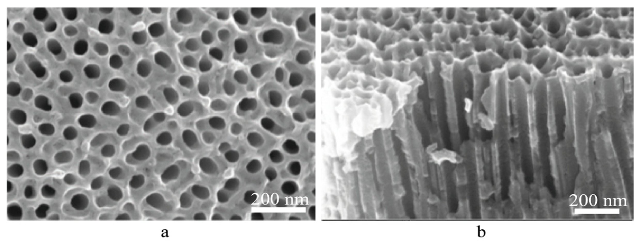
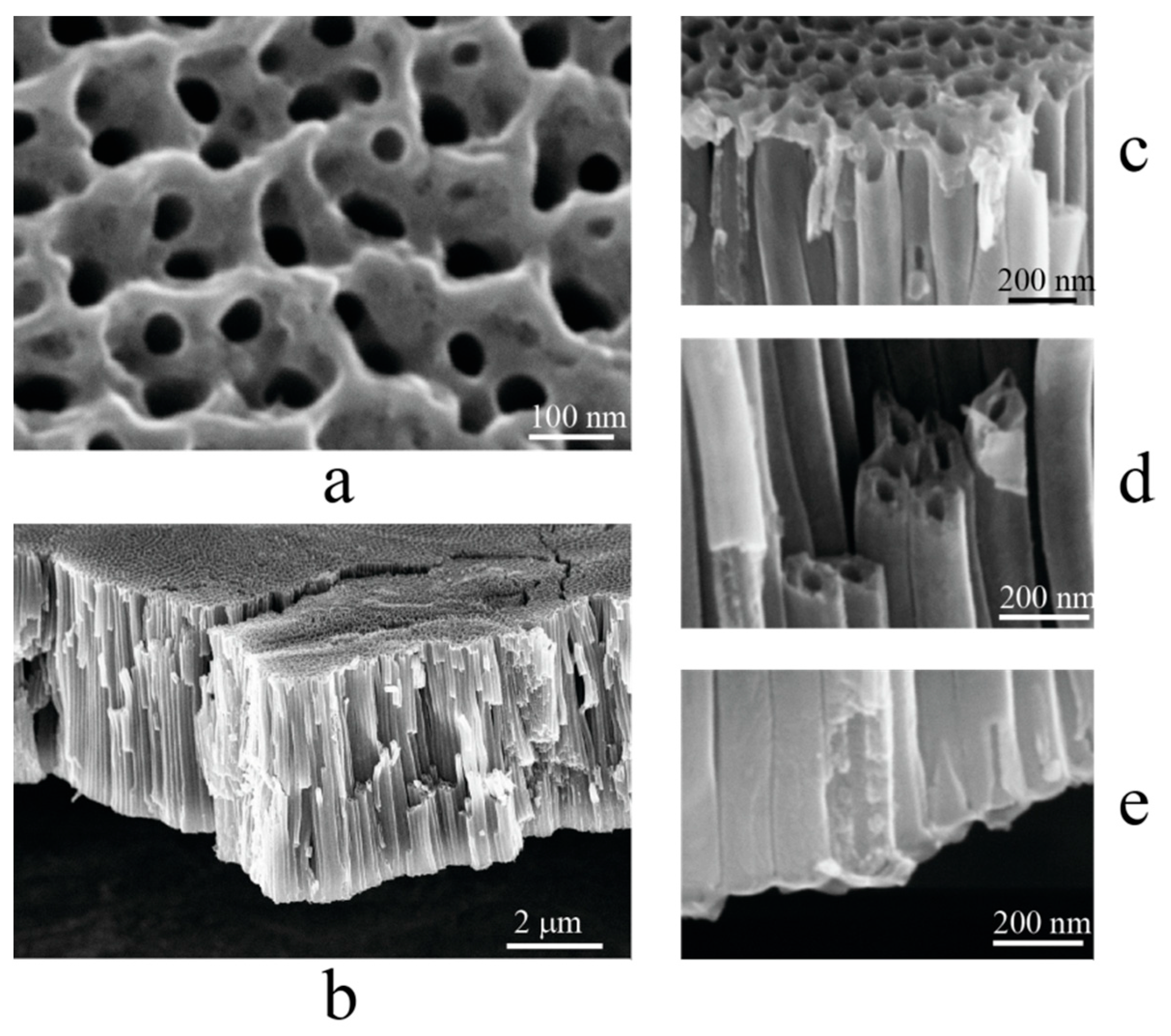
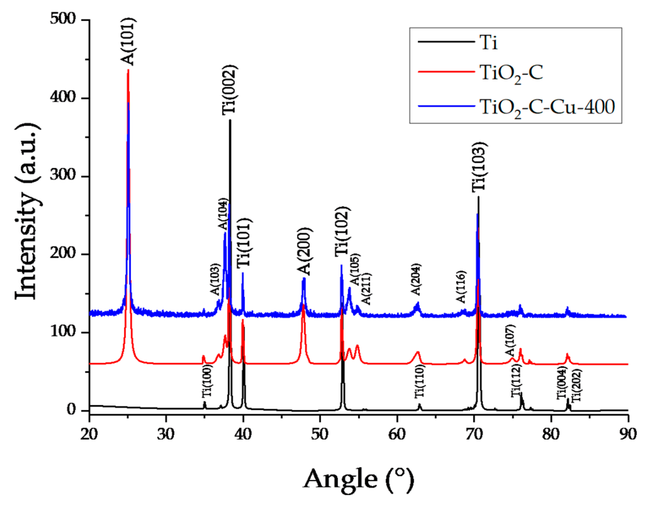
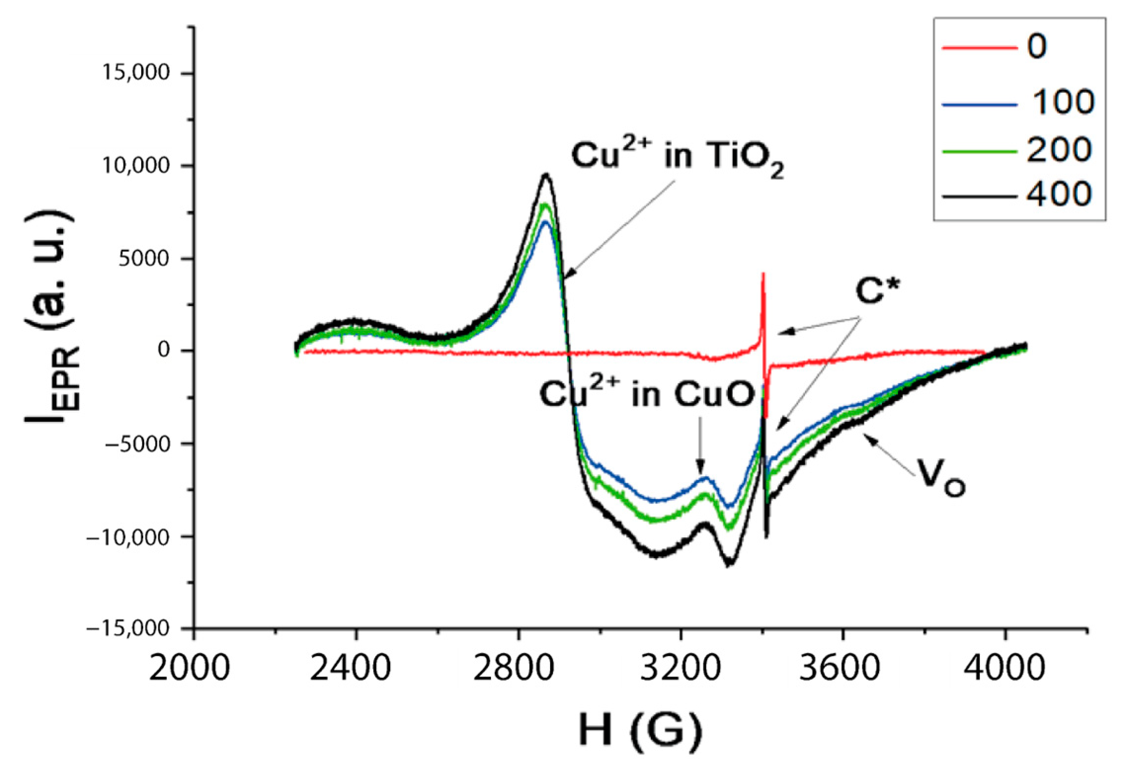
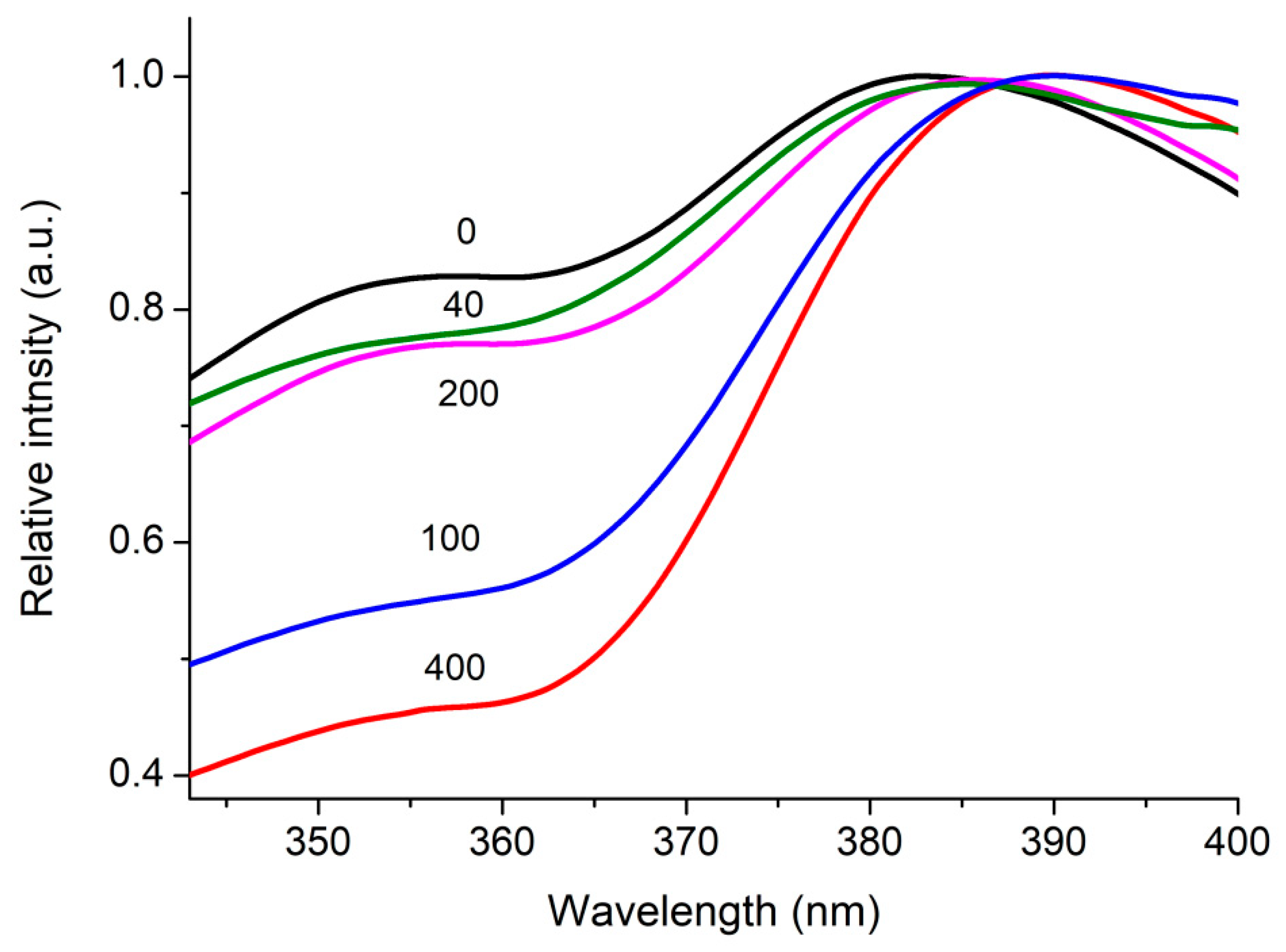
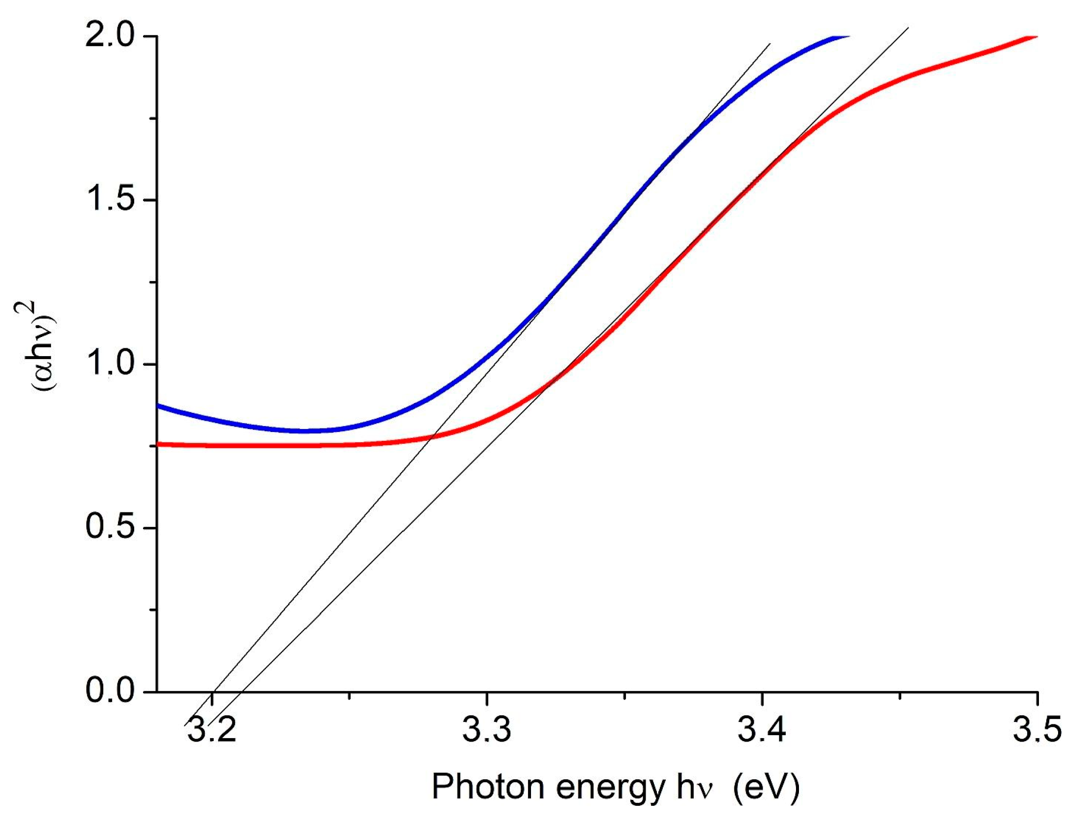
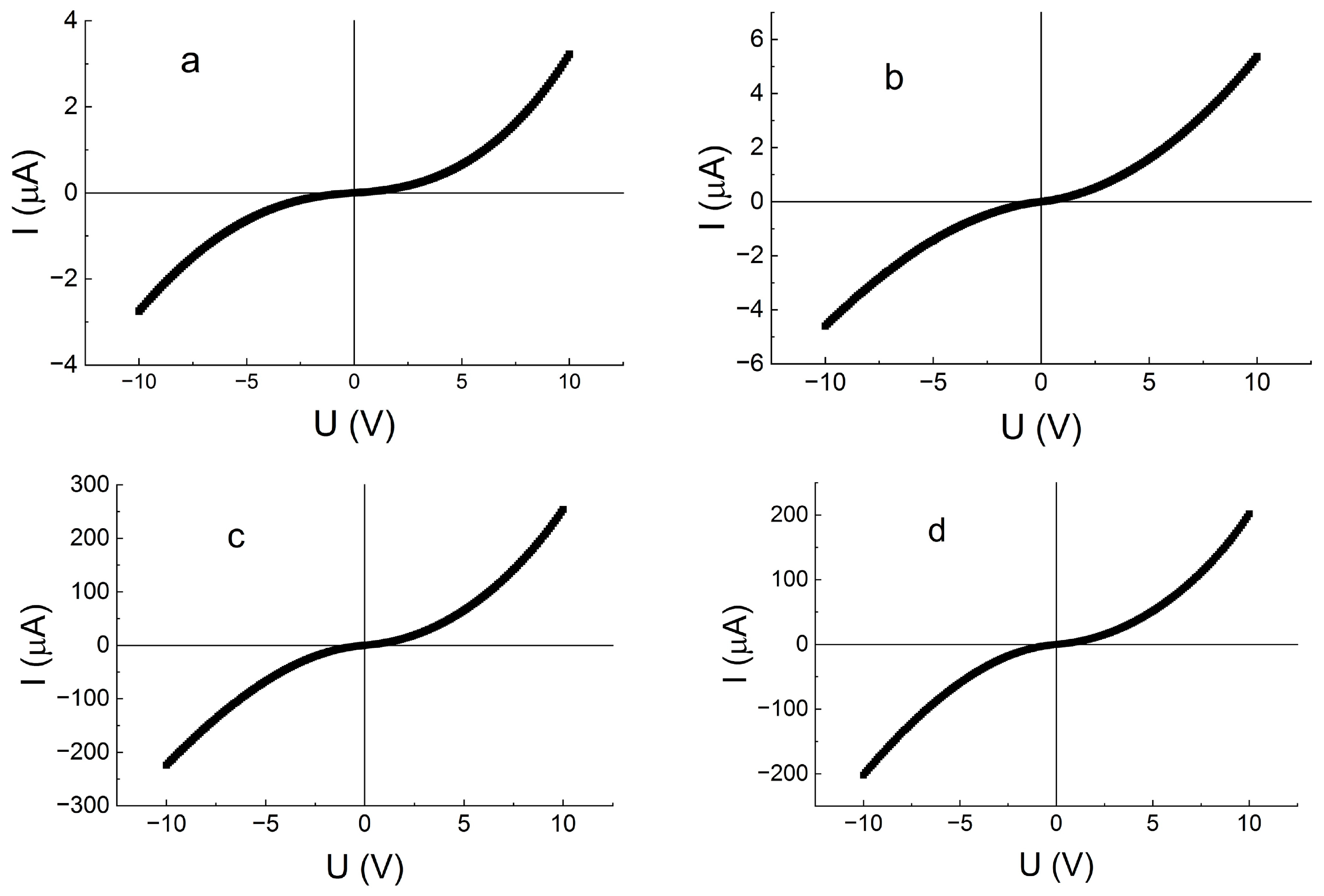
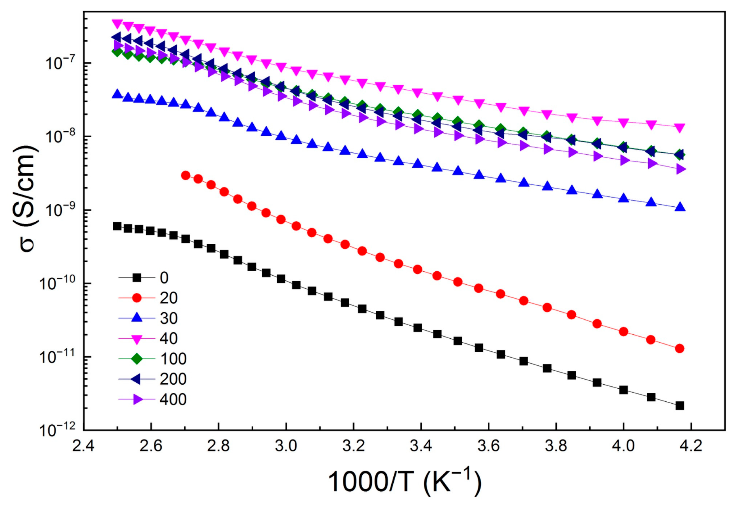
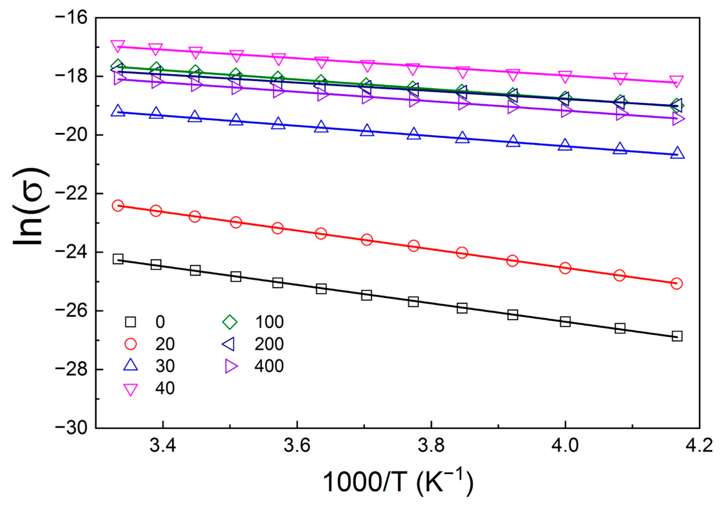
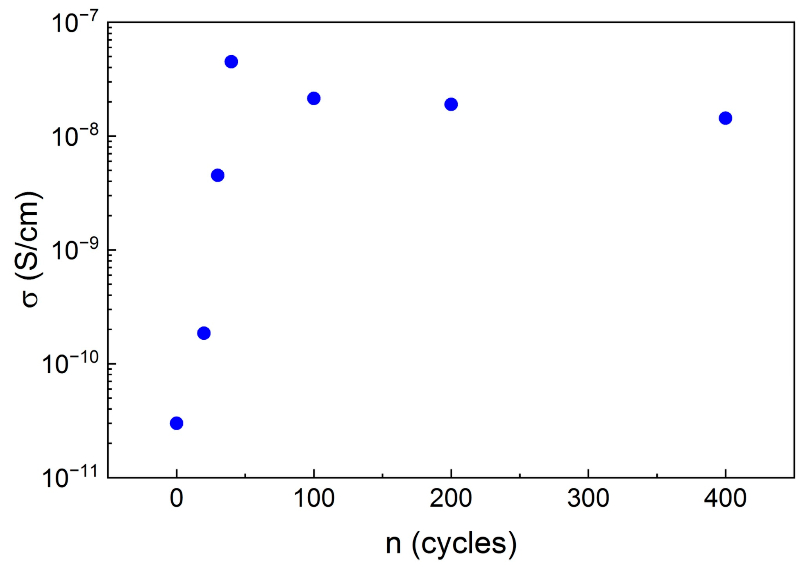
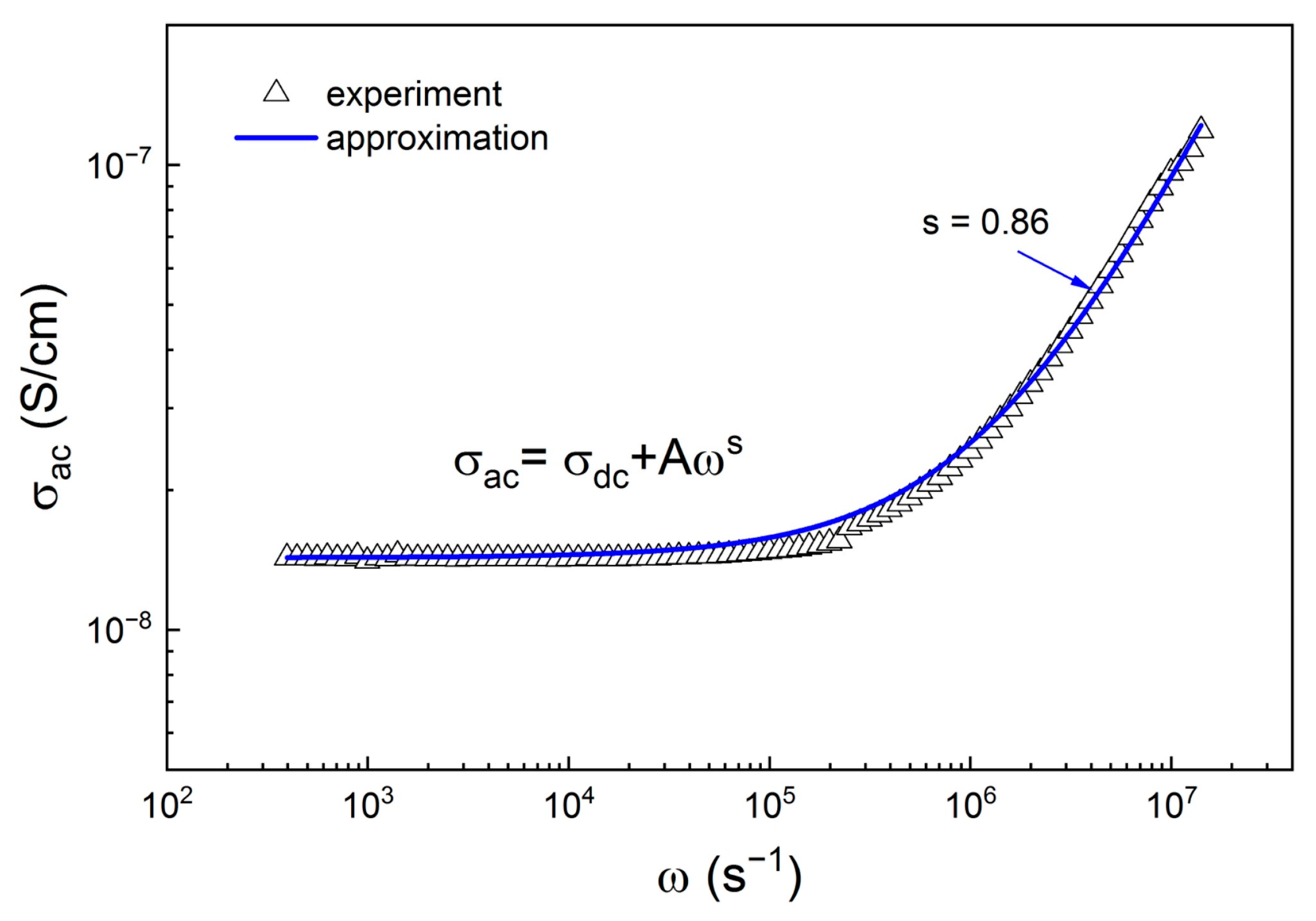
2. Results and Discussion

Figure 1, Figure 2 and Figure 3 show the SEM images of the original samples and prepared samples with numbers of Cu deposition cycles of 40 and 400 as an example.
The average value of the inner diameters of the nanotubes is ~70 nm. As follows from the presented micrographs, for all modified samples under these experimental conditions, no visible copper nanoparticles on the nanotube surfaces are observed. The morphology of the nanotube arrays itself does not undergo significant changes.
When the accelerating voltage is increased up to 30 kV, copper agglomerated into large micron-sized particles is detected on the surface of the samples (Figure 4).
As follows from Figure 4, copper is distributed unevenly over the surface of the samples, and it can form micron-sized agglomerates. The energy-dispersive X-ray spectroscopy technique was used to analyze the chemical composition of the samples (accelerating voltage—30 kV; scanning depth—5.2 µm). The TiO2-C-Cu-400 samples have the following elemental composition (in at.%): C—6.02; Ti—25.92; O—62.08; Cu—3.92.
Time-of-flight secondary ion mass spectrometry (TOF-SIMS) was used for cooper detection. TOF-SIMS is a highly sensitive method which allows you to register elements with concentrations up to 10 ppb (2016 EAG, Inc. M-006916 Houston, TX, USA). To confirm the presence of copper, the 0 and 400 cycle samples were analyzed by TOF-SIMS. Fragments of integrated mass spectra are presented in Figure 5a,b.
From the presented results of TOF SIMS it can be seen that the intensity of the copper signal of TiO2-C-Cu with 400 copper deposition cycles is about 4·102. Despite the qualitative nature of the TOF SIMS results, from experimental experience, we know that a Cu+ intensity value of less than 103 corresponds to concentrations of the element on the surface of the material of less than 1 at.%.
Figure 6 shows the phase composition of the prepared samples according to the X-ray diffraction (XRD) analysis. As can be seen, the main peaks of the crystalline phase of anatase are observed for both TiO2-C and TiO2-C-Cu-400 samples, while rutile is not registered (Figure 6).
Electron paramagnetic resonance is a powerful tool to determine the types of states with an unpaired electron, which play a key role in all physical and chemical processes, such as the valence states of doping elements and their local environment in the host matrices, e.g., [38,39,40,41,42]. The advantage of the EPR method is its high sensitivity compared to Raman, XRD, XPS, and other methods. Therefore, we used EPR for the detection of copper ions. The EPR spectra of TiO2-C-Cu samples consist of several EPR lines (Figure 7). The EasySpin function package 6.0.6 [43] was applied to correctly determine the main parameters of the EPR signals.
Let us discuss the data presented in Figure 7. First, a strong EPR signal from copper ions Cu2+ embedded in the structure of titania (g = 2.3212 ± 0.0005, line width ∆H = 330 G) [40,42,44] is registered in the magnetic field range of 2600–3100 G. Various defects (e.g., oxygen and titanium vacancies), are present on the surface of nanostructured titanium oxide, which have been identified by EPR [38,39,40,41,42,44]. Since the ionic radii of titanium and copper are close, copper can be embedded in titanium vacancies on the surface, and Cu2+ ions are formed on the surface of titania in substitution positions [40,42].
In the magnetic field range of 3000–3300 G, an EPR signal is observed with g = 2.1635 ± 0.0005, line width ∆H = 320 G from Cu2+, and copper ions in the CuO phase [42]. The latter indicates partial oxidation of metallic copper deposited on the surface. It is noted that such a large width of EPR lines from copper ions may be due to unresolved hyperfine splitting (the spin of the copper nucleus is 3/2) as well as dipole–dipole and/or exchange interactions. Therefore, a correct calculation of the concentration of copper ions in the samples is impossible.
In addition, in the right part of the EPR spectrum (interval H = 3406 G), there is a narrow line from dangling carbon bonds (g = 2.0027 ± 0.0005, ∆H = 7 G), which is also observed in the original samples (not modified by copper) (Figure 7) [28]. The source of carbon in our samples is ethylene glycol, which is a part of the electrolyte. During the anodization process, the decomposition products of ethylene glycol (carboxylic acids, ethylene glycol complexes) are retained in the volume of the inner layer of the nanotubes [26]. The resulting oxide is amorphous, and a thermal treatment is necessary for its crystallization. During thermal treatment in air, organic compounds are oxidized, and some of these oxidation products are retained in titania nanotubes. Time-of-flight mass spectrometry detected ionic fragments, the most common of which was TiC2O, indicating the presence of Ti-C bonds in our samples [26] as well as pointing to the substitution of oxygen by carbon in the titania lattice. Using the highly sensitive EPR method, we obtained additional important information about other carbon states in the investigated samples. Considering that the EPR line from carbon defects (dangling carbon bonds) observed in the EPR spectrum is isotropic (Figure 5), it can be assumed that these defects are in a disordered carbon phase located in the surface or near-surface region. Similar results reporting the presence of defects and disordered carbon sites were obtained, for example, in [29]. We calculated the concentration of dangling carbon bonds, which amounted to 1.3∙1015 g−1 and coincided for all samples of this series and the initial samples, indicating that there was no interaction between copper ions embedded in titanium dioxide nanotubes and internal defects in the form of dangling carbon bonds. Due to the low concentration of carbon defects and, consequently, the small amount of disordered carbon phase, it is not possible to detect them using other methods. Finally, in the field region of H = 3630 G, a shoulder corresponding to Ti3+ centers (g = 1.9712) is observed in the spectrum (Figure 5) [38]. We assume that Ti3+ centers are also localized in the near-surface disordered layer.
The spectra of light diffusely reflected from samples with different numbers of copper deposition cycles were studied to determine the band gap energy of the samples. The spectra in Figure 8 show the different absorption of light by the samples in the wavelength region near the absorption threshold related to the band gap Eg of the material. The diffuse reflectance spectra show that there is an enhancement in optical absorption in the UV region. It is known that CuO can absorb UV radiation [45]. The results of EPR spectroscopy show the presence of CuO phase. Thus, the enhancement in optical absorption in the UV region can be explained by the oxidation of copper.
The Eg values can be obtained from these spectra using the Kubelka–Munk theory [46]. For this purpose, it is necessary to determine the reflection coefficient R for each sample. R = RD/R, where RD is the reflection coefficient of the sample under consideration, and R is the diffuse reflection of an “absolutely white body” (in practice, such bodies can be those whose surface is covered with a thin layer of barium sulfate, carbonate or magnesium oxide).
The point is that in diffuse reflectance spectroscopy, as in absorption and emission spectroscopy, it is necessary to eliminate the wavelength dependence of the instrument response. These spectral features of the equipment, as well as the absorption, are taken into account in the measurement of the diffuse reflection of a “perfectly white body”. The Kubelka–Munk function is then constructed for each sample.
αF(R) = /S = (1 − R)2/2 R,
where α is equal to the absorption coefficient divided by the scattering coefficient S (R is described earlier in this paper). Further, in the calculations, instead of the absorption coefficient, the Kubelka–Munk function is used, assuming that in the considered narrow wavelength range, the value S can be considered to be equal to a constant [47].
To determine the band gap for the interband direct transitions, the experimental data are presented in the form of the following dependence:
α(ћω)2 ≈ (F(Rћω)2 = A2(ћω − Eg),
which must be linear within certain limits. In this equation, ћω is the photon energy, Eg is the bandgap of the material, and A is a constant. The Eg value is determined by extrapolating a straight line to the intersection with the x-axis. Figure 9 shows, as an example, a scheme to determine the optical band gap for the initial TiO2-C samples and for the TiO2-C-Cu with 400 copper deposition cycles using the Kubelka–Munk function.
It can be seen from Figure 9 that the band gap is 3.20 eV for TiO2-C. The Eg values for the TiO2-C-Cu samples were determined in a similar way. All samples show similar Eg values (Table 1).
The accuracy of determining Eg from the plots is not worse than 0.01 eV. However, taking into account the possible error introduced into the final result by the dependence of the light scattering function S on the wavelength, we believe that the final error in determining Eg is ±0.05 eV. More detailed information can be found in the Supplementary Materials. Thus, it can be stated that the band gap of the studied samples practically coincides with the accuracy of the measurement error. This means that the introduction of Cu ions by the electrochemical technique into TiO2-C nanotubes basically did not affect the band gap of the samples. The introduction of Cu also changes the light absorption of the material in the visible region. The additional light absorption was calculated from the change in the diffuse light reflectance spectra and is shown in Figure 10. As can be seen, a significant increase in absorption in the visible region is observed after the introduction of copper ions. This indicates that we have overcome the disadvantage associated with the large band gap of titanium dioxide. This is consistent with the detection of defects in TiO2—copper ions Cu2+ according to EPR data, which create energy levels in the band gap and contribute to the absorption of impurities. Figure 8 shows that in the region of short wavelengths, the slope of the graph/plot differs for samples with different copper content. This fact can also be related to the differences in the structure of the band gap (different spectra of local states in the band gap), which may be associated with the introduction of copper ions into the crystal lattice of titania. This result is in agreement with the EPR spectroscopy data presented above. In addition, metal particles on the surface of titanium oxide are plasmonic centers and can also enhance the absorption of visible light, which is important for practical applications [35].
We shall now discuss the features of charge carrier transport in the acquired nanocomposites. Using the method of measuring the sign of thermal EMF, it was found that all samples possess n-type conductivity. Figure 11 shows as an example of the the current–voltage characteristics of TiO2-C structures and TiO2-C-Cu structures with numbers of processing cycles of 20, 40, and 400, measured at room temperature after annealing of the samples. Similar characteristics were obtained for the other samples.
As can be seen from Figure 11, modification by copper does not lead to a noticeable change in the shape of the current–voltage characteristic, which for all samples have a symmetric and nonlinear character. The nonlinearity of the current–voltage characteristics of these structures, as mentioned earlier, is explained by the formation of a Schottky barrier at the interface of the samples with the upper and lower titanium electrodes.
Figure 12 shows the temperature dependences of TiO2-C and TiO2-C-Cu. As can be seen, these dependences have an activation character and can be described by the following dependence:
σ = σ 0 e E A k T
where σ 0 is a pre-exponential factor weakly dependent on temperature, k is the Boltzmann coefficient, and EA is the activation energy.
The temperature dependences of the conductivity measured for all studied structures are best described by the activation dependence in the temperature range below room temperature (240–300 K). These dependencies are shown in Figure 13 in ln σ (1000/T) coordinates.
The experimental data were approximated by the above law, as a result of which the conduction activation energies for all samples were calculated. The obtained values of conduction activation energy, as well as the values of conductivity at room temperature (300 K), are given in Table 2.
The activation energy of conductivity in n-type semiconductors, to which titanium dioxide belongs, is determined by the position of donor levels in the band gap. In the simplest case, when there is only one donor level with energy Ed and no compensating acceptor impurities, the activation energy EA = (Ec − Ed)/2, where Ec is the energy of the bottom of the conduction band. As can be seen from Table 2, the modification with copper leads to a change in the activation energy of conductivity. The activation energy is (0.27 ± 0.01) eV for TiO2-C and TiO2-C-Cu samples at a number of treatment cycles equal to 20. With further increasing the number of copper processing cycles, a sharp change in the activation energy is observed, which, for all other samples, takes close values in the range of 0.12–0.15 eV. This change in activation energy indicates a change in the band structure of TiO2-C samples as a result of modification by copper. In addition, it is clearly seen from Table 2, as well as from Figure 13, that modification with copper by the electrochemical method leads to an increase in conductivity. The dependence of conductivity at a temperature of 300 K on the number of copper treatment cycles is shown in Figure 14.
As seen from Figure 14, the modification by copper shows a sharp increase in conductivity by 3 orders of magnitude with an increase in the number of processing cycles from 0 to 40. After that, with a further increase in the number of cycles up to 400, the conductivity remains practically unchanged. The result obtained is fundamentally different from what was obtained earlier on samples modified with copper oxide by the SILAR method. It was previously shown that modification by copper oxide leads, on the contrary, to a decrease in conductivity [48]. We proposed a model explaining the decrease in electrical conductivity by the formation of TiO2/CuO heterojunctions. Nevertheless, the previously developed model is not suitable for explaining the increase in conductivity in this case. This increase, as well as a significant change in the activation energy, may indicate the formation of new donor levels in the band gap of titania, which arise as a result of the introduction of copper ions into the TiO2 structure. This donor level may correspond to various structural defects, such as Ti3+ centers, e.g., [49,50]. Using the EPR technique, it is shown that Ti3+ centers are present in copper-modified samples. These defects can be attributed to shallow donors [51] whose states are located in the band gap of titanium dioxide near the bottom of the conduction band. The significant decrease in the activation energy indicates that the donor level in the copper-modified samples is located closer to the bottom of the conduction band than the donor levels in the initial TiO2-C samples. The closer the donor level is to the bottom of the conduction band, the less energy is required for the thermal activation of electrons in the conduction band. This, in turn, leads to an increase in the concentration of free charge carriers in the band and, hence, an increase in conductivity.
To reveal the specific features of charge transfer processes in TiO2-C-Cu structures, the samples were studied at alternating currents by impedance spectroscopy. This method is less sensitive than DC conductivity measurement, which prevents it from being used for SILAR-modified samples due to their extremely low conductivity. Figure 15 shows the impedance hodographs, i.e., the dependences of the imaginary part of the impedance (-Im Z) on the real part (Re Z) for copper-modified samples, with numbers of processing cycles of 40 and 400. For the other samples, the dependencies are similar. As can be seen, the hodographs look like semicircles. This type of hodograph is described by a simple equivalent circuit consisting of a resistor (Rs) and a capacitor (Cs) connected in parallel (inset to Figure 15).
As an example, Figure 16 shows the dependence of AC conductivity σac on AC frequency ω obtained for TiO2-C-Cu samples with a number of processing cycles equal to 40. Similar results were obtained for the other copper-modified samples. It can be seen (Figure 16) that up to frequencies ~105 s−1, the conductivity is independent of the AC frequency, while at frequencies of 105–107 s−1, the conductivity increases with frequency according to a power law. AC conductivity can be described by Jonscher’s power law [52]:
σ a c = σ d c + A ω s
where σ a c is DC conductivity, A is a constant, and s is an exponent degree. The frequency dependence of conductivity was approximated by the above equation, and the results of the approximation are also shown in the plot. The value s = 0.86 was obtained for the exponent degree. The power law dependence of electrical conductivity on frequency indicates a hopping mechanism of conductivity. An exponent degree close to 0.8 is typical for conductivity due to electron tunneling between defective states located near the Fermi level, which is described by the quantum mechanical tunneling (QMT) model [53,54]. The fact that at low frequencies the conductivity is frequency-independent indicates that the charge transfer occurs along the delocalized states of the conduction band. Consequently, at DC and frequencies ω < 105 s−1, in the studied samples it exceeds the usual band conduction due to the thermal transfer of electrons from impurity levels into the conduction band and their delocalization. At higher frequencies, electron jumps from one impurity to another begin to dominate without the participation of the band of delocalized states.
In order to analyze the prospects of using the obtained TiO2-C-Cu samples in the fields of photoelectrochemistry and photocatalysis, we investigated the effect of copper treatment cycles on the magnitude of photocurrent when the samples were illuminated in different spectral ranges. The results obtained are presented in Figure 17.
The photocurrent values for illumination with UV light (λ > 250 nm) and in the visible region (λ > 430 nm) differ by two orders of magnitude. This difference is due to the fact that when irradiated with light with a wavelength of 250 nm (4.96 eV), the energy of the incident photons is sufficient to transfer photogenerated electrons from the valence band to the conduction band directly (Eg~3 eV). When irradiated with light with wavelengths of 430 nm (2.88 eV), the energy of the incident photons is not enough for such electron transfer. In this regard, when illuminating samples with visible light (wavelength of approximately 430 nm), the photocurrent value is determined by the ionization of impurity levels in the conduction band and the subsequent transfer of electrons through the level–band transition. The number of electrons available for ionization in this case is much smaller, which leads to such a colossal difference in photocurrents when illuminated by UV and visible light.
It is evident that under illumination in both ranges—broad-band UV-Vis (λ > 250 nm) (Figure 17a) and visible light (λ > 430 nm) (Figure 17b)—the dependence of the photocurrent value on the number of copper processing cycles correlates with the similar dependence of conductivity value (Figure 14 and Figure 17). Thus, it can be assumed that the initial growth in conductivity and photocurrent with an increasing number of copper treatment cycles is due to the growth of donor centers such as Ti3+ centers, while a further slight decrease in conductivity and photocurrent can be explained by the capturing of charge carriers caused by Cu2+-type defects, the intensity of the EPR signal from which increases with an increasing number of copper treatment cycles (Figure 7).

3. Materials and Methods

3.1. Formation of Carbon-Doped Titania Nanotubes

The synthesis of titanium oxide nanotubes doped with carbon (TiO2-C) was carried out by the two-stage electrochemical oxidation of Ti-foil. The anodic oxidation was carried out in an ethylene glycol-based electrolyte (0.3 wt. % NH4F and 2% deionized water) at 20 °C using a thermostated base. Ethylene glycol served as a carbon source to dope the samples with carbon. A platinum grid was used as a counter-electrode. The preliminary preparation consisted of etching the Ti-foil in a solution of HF:HNO3:H2O (3:2:15). At the first stage of forming TiO2-C arrays, the pre-prepared Ti-foil was anodized in potentiostatic mode at constant voltage of 60 V for 30 min. This was followed by cathodic polarization in a 5% H2SO4 solution to separate the formed titania layer from the substrate. The first stage is necessary to achieve a more uniform thickness of the nanotube layer. Then, the second stage of the anodization process was carried out at 60 V for 60 min, resulting in the formation of arrays of carbon-doped TiO2 nanotubes with a length of 5–6 μm long, located on the foil perpendicular to the substrate. After anodic oxidation, all samples were rinsed with ethanol. To crystallize the amorphous structure of nanotubes, the samples were annealed at 450 °C in a muffle furnace for 60 min.

3.2. Synthesis of TiO2-C-Cu Nanocomposite by Electrochemical Deposition of Copper Nanoparticles

The copper precipitation solution was prepared as follows: 0.4 M copper sulfate (CuSO4) was added to 3 M of lactic acid aqueous solution and stirred. The pH was then adjusted to 3–4 with 5 M aqueous NaOH solution (~20 mL of aqueous NaOH solution per 200 mL solution). Copper was then deposited on the TiO2-C surface at a temperature of 20 °C and a potential of −1.5 V relative to Ag/AgCl (3 M). A platinum plate served as a counter-electrode. The deposition was conducted in pulse mode, when the pulse and no-pulse time were 10 ms and 1 s, respectively (1 deposition cycle). After the deposition process, the samples were rinsed with deionized water and dried in an air stream. Two series of TiO2-C-Cu samples were prepared with different numbers of deposition cycles: 10, 20, 30 and 40, 100, 200, 400.
The stability of the investigated materials was determined by applying well-established synthesis technologies in their preparation. Such technologies allow us to obtain samples with physical–chemical properties that are stable over time, which is confirmed by a large number of repeated experiments on reproducibility depending on the time of sample storage.

3.3. Microscopy, EDX, XRD

Morphological characterization and chemical composition analysis were performed by a Helios G4CX scanning electron microscope (Thermo Fisher Scientific, Waltham, MA, USA) equipped with an EDS (EDAX Octane Elite Super) attachment. The modes were accelerating voltages of 10 and 30 kV, and imaging was performed at angles of 0 and 70 degrees. A Rigaku MiniFlex X-ray diffractometer (Rigaku, Tokyo, Japan) (Cu Ka radiation at 1.54 Å) was used to analyze the obtained samples.

3.4. Secondary Ion Mass Spectrometry

The images were studied by secondary ion mass spectrometry using a ToF.SIMS 5 time-of-flight mass spectrometer from the German company ION-TOF (Münster, Germany). The energy of the Bi+ analytical beam was 30 keV. The number of accumulations was 5 scans. The measurements were carried out in sputtering modes with O2+ ions with an energy of 500 eV while we analyzed the positive secondary ions. The spray area was 300 × 300 microns.

3.5. Optical Measurement

The diffuse light reflectance spectra were obtained using a Perkin Elmer LS-55 spectrometer (Waltham, MA, USA), which can record diffuse light scattering in the range of 200 to 800 nm with spectral slit widths from 2.5 to 20 nm.

3.6. EPR Spectroscopy

Electron paramagnetic resonance (EPR) spectra were recorded with a Bruker ELEXSYS E500 EPR spectrometer (Bruker, Berlin, Germany) (X-band). All EPR measurements were performed using the facilities of the Center for Collective Use of the Faculty of Physics, Moscow State University.

3.7. Conductivity Measurement

The electrical properties of the investigated samples were measured using a Keithley 6487 picoammeter (Keithley, Solon, OH, USA). The volt-ampere characteristics and temperature dependences of conductivity were obtained on a sandwich-type structure. The lower electrode was a titanium substrate, on which the nanotubes were directly formed. The upper metal electrode, with a size of 3 × 4 mm2, was also made of the substrate material and pressed onto the surface of titanium dioxide nanotubes. The thickness of the TiO2 nanotube layer, which was used to calculate the specific conductivity, was 5 μm. The temperature was controlled by an ARS DE-204SE helium cryostat. To stabilize the electrical properties, the samples were annealed at T = 400 K in a vacuum for 1.5 h before measurements. Conductivity measurements were performed at a pressure of p = 10 mbar within a temperature range of 240 to 400 K. The constant voltage applied to the sample was 10 V. The AC conductivity of the structures was studied by an HP4192A impedance analyzer in the frequency range of 5 Hz to 13 MHz at room temperature with an AC signal amplitude of 0.5 V.

3.8. Photocurrent Measurement

The photoactivity of the acquired samples was studied using a Zolix photoelectrochemical measurement system (Zolix, Beijing, China) in 0.1 M Na2SO4 with a platinum counter-electrode and a silver chloride reference electrode (3 M KCl). A xenon lamp (total power of 500 W) was used as a light source with a power of light incident on the sample of ~100 mW/cm2. For measurements in the visible light range, an optical filter was used to cut off radiation with a wavelength of less than 430 nm. Photocurrent measurements were carried out at a constant potential relative to the silver chloride electrode by alternately switching the light on and off.

4. Conclusions

TiO2-C-Cu nanocomposites were prepared by the electrochemical method. According to the SEM study, the average value of the inner diameter of the nanotubes was about 70 nm. The copper species on the surface of the titania nanotubes agglomerated into large micron-sized particles. The band gap Eg of the investigated samples was estimated using the diffuse light reflection technique and estimated to be 3.2 eV. The optical Eg was found to be independent of the number of Cu deposition cycles. An important result is that the samples with copper showed an increase in absorption in the visible region.
In TiO2-C-Cu samples, copper ions replacing titanium ions in the titanium dioxide lattice and Cu ions in the CuO phase were detected by the EPR method, indicating partial oxidation of the deposited copper particles. Dangling carbon bonds found in the original TiO2-C nanotubes were also present in the modified samples.
The study of the electrophysical properties of TiO2-C-Cu nanocomposites showed that the modification with copper led to a significant increase in conductivity. This growth was probably due to the incorporation of copper ions into the TiO2 structure, which led to the formation of new Ti3+ donor states that create levels in the band gap of TiO2-C-Cu. It was also shown that at DC and at low AC frequencies, conductivity is related to the movement of electrons along the conduction band, while at high frequencies the hopping mechanism of conductivity prevails.
Thus, we conducted a detailed study of the electronic properties of TiO2-C-Cu nanocomposites for the first time and found a sharp increase in the values of both conductivity and photocurrent, as well as a change in the conductivity mechanism depending on the frequency of current. The results obtained open new possibilities for the use of TiO2-C-Cu nanocomposites in the field of photoelectrochemistry.

Supplementary Materials

The following supporting information can be downloaded at: https://www.mdpi.com/article/10.3390/catal15060572/s1, Figure S1: Graphical construction to determine the band gap for the TiO2-C (blue curve) and for the TiO2-C-Cu-400 samples (red curve).

Author Contributions

Conceptualization, E.A.K. and M.N.M.; methodology, E.A.K. and A.I.K.; software, E.V.K. and T.P.S.; validation, V.B.Z., A.S.I. and E.A.K.; formal analysis, A.S.I. and G.V.T.; investigation, M.N.M., E.V.K., V.B.Z., T.P.S., E.A.K. and G.V.T.; data curation, E.A.K.; writing—original draft preparation, E.A.K., M.N.M. and E.V.K.; writing—review and editing, E.A.K. and A.I.K.; visualization, M.N.M. and A.I.K.; supervision, E.A.K. All authors have read and agreed to the published version of the manuscript.

Funding

The formation of TiO2-C-Cu samples, along with photoelectrochemical, XRD, SEM, and EDX studies, was performed in the research laboratory ‘Photon Sensorics and Plasmonic Materials’ as part of the state task FSMR-2024-0012 under Supplementary Agreement No. 075-03-2024-061/3, dated 15.04.2024. The EPR investigation was performed as a part of the Program of Fundamental Research of the Russian Federation (No. 125012200595-8). Conductivity measurements were supported by the Russian Science Foundation grant No. 24-19-00402, https://rscf.ru/en/project/24-19-00402/, accessed on 1 June 2025. German V. Trusov is grateful for the financial support the Priority-2030 Program of NUST “MISiS” (grant No. K2-2022-022).

Institutional Review Board Statement

Not applicable.

Informed Consent Statement

Not applicable.

Data Availability Statement

The data presented in this study are available on request.

Acknowledgments

The EPR measurements were performed using the facilities of the Collective Use Center at the Moscow State University.

Conflicts of Interest

The authors declare no conflicts of interest.

References

  1. Chen, D.; Cheng, Y.; Zhou, N.; Chen, P.; Wang, Y.; Li, K.; Huo, S.; Cheng, P.; Peng, P.; Zhang, R.; et al. Photocatalytic Degradation of Organic Pollutants Using TiO2-Based Photocatalysts: A Review. J. Clean. Prod. 2020, 268, 121725. [Google Scholar] [CrossRef]
  2. Ochiai, T.; Fujishima, A. Photoelectrochemical Properties of TiO2 Photocatalyst and Its Applications for Environmental Purification. J. Photochem. Photobiol. C Photochem. Rev. 2012, 13, 247–262. [Google Scholar] [CrossRef]
  3. Arifin, K.; Yunus, R.M.; Minggu, L.J.; Kassim, M.B. Improvement of TiO2 Nanotubes for Photoelectrochemical Water Splitting: Review. Int. J. Hydrogen Energy 2021, 46, 4998–5024. [Google Scholar] [CrossRef]
  4. Woan, K.; Pyrgiotakis, G.; Sigmund, W. Photocatalytic Carbon-Nanotube–TiO2 Composites. Adv. Mater. 2009, 21, 2233–2239. [Google Scholar] [CrossRef]
  5. Zubair, M.; Kim, H.; Razzaq, A.; Grimes, C.A.; In, S.-I. Solar Spectrum Photocatalytic Conversion of CO2 to CH4 Utilizing TiO2 Nanotube Arrays Embedded with Graphene Quantum Dots. J. CO2 Util. 2018, 26, 70–79. [Google Scholar] [CrossRef]
  6. Muiva, C.M.; Maabong, K.; Moditswe, C. CuO Nanostructured Thin Films Synthesised by Chemical Bath Deposition on Seed Layers Deposited by Successive Ionic Layer Adsorption and Reaction and Chemical Spray Pyrolysis Techniques. Thin Solid Films 2016, 616, 48–54. [Google Scholar] [CrossRef]
  7. Tang, X.; Ren, L.; Sun, L.; Tian, W.; Cao, M.; Hu, C. A Solvothermal Route to Cu2O Nanocubes and Cu Nanoparticles1. Chem. Res. Chin. Univ. 2006, 22, 547–551. [Google Scholar] [CrossRef]
  8. Rawool, S.A.; Yadav, K.K.; Polshettiwar, V. Defective TiO2 for Photocatalytic CO2 Conversion to Fuels and Chemicals. Chem. Sci. 2021, 12, 4267–4299. [Google Scholar] [CrossRef]
  9. Sviridova, T.V.; Sadovskaуa, L.Y.; Konstantinova, E.A.; Belyasova, N.A.; Kokorin, A.I.; Sviridov, D.V. Photoaccumulating TiO2-MoO3, TiO2-V2O5, and TiO2-WO3 Heterostructures for Self-Sterilizing Systems with the Prolonged Bactericidal Activity. Catal. Lett. 2019, 149, 1147–1153. [Google Scholar] [CrossRef]
  10. Kong, L.; Wang, C.; Zheng, H.; Zhang, X.; Liu, Y. Defect-Induced Yellow Color in Nb-Doped TiO2 and Its Impact on Visible-Light Photocatalysis. J. Phys. Chem. C 2015, 119, 16623–16632. [Google Scholar] [CrossRef]
  11. Wei, Y.; Huang, Y.; Fang, Y.; Zhao, Y.; Luo, D.; Guo, Q.; Fan, L.; Wu, J. Hollow Mesoporous TiO2/WO3 Sphere Heterojunction with High Visible-Light-Driven Photocatalytic Activity. Mater. Res. Bull. 2019, 119, 110571. [Google Scholar] [CrossRef]
  12. Liu, J.; Luo, Z.; Mao, X.; Dong, Y.; Peng, L.; Sun-Waterhouse, D.; Kennedy, J.V.; Waterhouse, G.I.N. Recent Advances in Self-Supported Semiconductor Heterojunction Nanoarrays as Efficient Photoanodes for Photoelectrochemical Water Splitting. Small 2022, 18, 2204553. [Google Scholar] [CrossRef]
  13. Faisal, M.; Harraz, F.A.; Ismail, A.A.; El-Toni, A.M.; Al-Sayari, S.A.; Al-Hajry, A.; Al-Assiri, M.S. Novel Mesoporous NiO/TiO2 Nanocomposites with Enhanced Photocatalytic Activity under Visible Light Illumination. Ceram. Int. 2018, 44, 7047–7056. [Google Scholar] [CrossRef]
  14. Matos, J.; García, A.; Zhao, L.; Titirici, M.M. Solvothermal Carbon-Doped TiO2 Photocatalyst for the Enhanced Methylene Blue Degradation under Visible Light. Appl. Catal. A Gen. 2010, 390, 175–182. [Google Scholar] [CrossRef]
  15. Hua, L.; Yin, Z.; Cao, S. Recent Advances in Synthesis and Applications of Carbon-Doped TiO2 Nanomaterials. Catalysts 2020, 10, 1431. [Google Scholar] [CrossRef]
  16. Kacica, C.T.; Biswas, P. Improved Conductivity and Ionic Mobility in Nanostructured Thin Films via Aliovalent Doping for Ultra-High Rate Energy Storage. Nanoscale Adv. 2020, 2, 2160–2169. [Google Scholar] [CrossRef]
  17. Ahmad, A.A.; Alakhras, L.A.; Al-Bataineh, Q.M.; Telfah, A. Impact of Metal Doping on the Physical Characteristics of Anatase Titanium Dioxide (TiO2) Films. J. Mater. Sci. Mater. Electron. 2023, 34, 1552. [Google Scholar] [CrossRef]
  18. Mohajernia, S.; Hejazi, S.; Andryskova, P.; Zoppellaro, G.; Tomanec, O.; Zboril, R.; Schmuki, P. Conductive Cu-Doped TiO2 Nanotubes for Enhanced Photoelectrochemical Methanol Oxidation and Concomitant Hydrogen Generation. ChemElectroChem 2019, 6, 1244–1249. [Google Scholar] [CrossRef]
  19. Su, J.; Li, Z.; Zhang, Y.; Wei, Y.; Wang, X. N-Doped and Cu-Doped TiO2-B Nanowires with Enhanced Photoelectrochemical Activity. RSC Adv. 2016, 6, 16177–16182. [Google Scholar] [CrossRef]
  20. Hua, Z.; Dai, Z.; Bai, X.; Ye, Z.; Wang, P.; Gu, H.; Huang, X. Copper Nanoparticles Sensitized TiO2 Nanotube Arrays Electrode with Enhanced Photoelectrocatalytic Activity for Diclofenac Degradation. Chem. Eng. J. 2016, 283, 514–523. [Google Scholar] [CrossRef]
  21. Miyauchi, M.; Sunada, K.; Hashimoto, K. Antiviral Effect of Visible Light-Sensitive CuxO/TiO2 Photocatalyst. Catalysts 2020, 10, 1093. [Google Scholar] [CrossRef]
  22. Motola, M.; Hromadko, L.; Prikryl, J.; Sopha, H.; Krbal, M.; Macak, J.M. Intrinsic Properties of High-Aspect Ratio Single- and Double-Wall Anodic TiO2 Nanotube Layers Annealed at Different Temperatures. Electrochim. Acta 2020, 352, 136479. [Google Scholar] [CrossRef]
  23. Low, J.; Qiu, S.; Xu, D.; Jiang, C.; Cheng, B. Direct Evidence and Enhancement of Surface Plasmon Resonance Effect on Ag-Loaded TiO2 Nanotube Arrays for Photocatalytic CO2 Reduction. Appl. Surf. Sci. 2018, 434, 423–432. [Google Scholar] [CrossRef]
  24. Nischk, M.; Mazierski, P.; Gazda, M.; Zaleska, A. Ordered TiO2 Nanotubes: The Effect of Preparation Parameters on the Photocatalytic Activity in Air Purification Process. Appl. Catal. B 2014, 144, 674–685. [Google Scholar] [CrossRef]
  25. Dronov, A.; Gavrilin, I.; Kirilenko, E.; Dronova, D.; Gavrilov, S. Investigation of Anodic TiO2 Nanotube Composition with High Spatial Resolution AES and ToF SIMS. Appl. Surf. Sci. 2018, 434, 148–154. [Google Scholar] [CrossRef]
  26. Gavrilin, I.; Dronov, A.; Volkov, R.; Savchuk, T.; Dronova, D.; Borgardt, N.; Pavlikov, A.; Gavrilov, S.; Gromov, D. Differences in the Local Structure and Composition of Anodic TiO2 Nanotubes Annealed in Vacuum and Air. Appl. Surf. Sci. 2020, 516, 146120. [Google Scholar] [CrossRef]
  27. Yuferov, Y.V.; Popov, I.D.; Zykov, F.M.; Suntsov, A.Y.; Baklanova, I.V.; Chukin, A.V.; Kukharenko, A.I.; Cholakh, S.O.; Zhidkov, I.S. Study of the Influence of Anodizing Parameters on the Photocatalytic Activity of Preferred Oriented TiO2 Nanotubes Self-Doped by Carbon. Appl. Surf. Sci. 2022, 573, 151366. [Google Scholar] [CrossRef]
  28. Savchuk, T.; Gavrilin, I.; Konstantinova, E.; Dronov, A.; Volkov, R.; Borgardt, N.; Maniecki, T.; Gavrilov, S.; Zaitsev, V. Anodic TiO2 Nanotube Arrays for Photocatalytic CO2 Conversion: Comparative Photocatalysis and EPR Study. Nanotechnology 2022, 33, 055706. [Google Scholar] [CrossRef]
  29. Ryu, M.-H.; Jung, K.-N.; Shin, K.-H.; Han, K.-S.; Yoon, S. High Performance N-Doped Mesoporous Carbon Decorated TiO2 Nanofibers as Anode Materials for Lithium-Ion Batteries. J. Phys. Chem. C 2013, 117, 8092–8098. [Google Scholar] [CrossRef]
  30. Zhu, J.; Zhao, X.; Xiao, M.; Liang, L.; Liu, C.; Liao, J.; Xing, W. The Construction of Nitrogen-Doped Graphitized Carbon–TiO2 Composite to Improve the Electrocatalyst for Methanol Oxidation. Carbon 2014, 72, 114–124. [Google Scholar] [CrossRef]
  31. Ghumro, S.S.; Lal, B.; Pirzada, T. Visible-Light-Driven Carbon-Doped TiO2-Based Nanocatalysts for Enhanced Activity toward Microbes and Removal of Dye. ACS Omega 2022, 7, 4333–4341. [Google Scholar] [CrossRef] [PubMed]
  32. Negi, C.; Kandwal, P.; Rawat, J.; Sharma, M.; Sharma, H.; Dalapati, G.; Dwivedi, C. Carbon-Doped Titanium Dioxide Nanoparticles for Visible Light Driven Photocatalytic Activity. Appl. Surf. Sci. 2021, 554, 149553. [Google Scholar] [CrossRef]
  33. Yang, Y.; Ni, D.; Yao, Y.; Zhong, Y.; Ma, Y.; Yao, J. High Photocatalytic Activity of Carbon Doped TiO2 Prepared by Fast Combustion of Organic Capping Ligands. RSC Adv. 2015, 5, 93635–93643. [Google Scholar] [CrossRef]
  34. Nogueira, M.V.; Lustosa, G.M.M.M.; Kobayakawa, Y.; Kogler, W.; Ruiz, M.; Monteiro Filho, E.S.; Zaghete, M.A.; Perazolli, L.A. Nb-Doped TiO2 Photocatalysts Used to Reduction of CO2 to Methanol. Adv. Mater. Sci. Eng. 2018, 2018, 7326240. [Google Scholar] [CrossRef]
  35. Kumar, A.; Choudhary, P.; Kumar, A.; Camargo, P.H.C.; Krishnan, V. Recent Advances in Plasmonic Photocatalysis Based on TiO2 and Noble Metal Nanoparticles for Energy Conversion, Environmental Remediation, and Organic Synthesis. Small 2022, 18, 2101638. [Google Scholar] [CrossRef]
  36. Li, Q.; Li, F. Recent Advances in Molecular Oxygen Activation via Photocatalysis and Its Application in Oxidation Reactions. Chem. Eng. J. 2021, 421, 129915. [Google Scholar] [CrossRef]
  37. Zhu, S.; Liang, S.; Tong, Y.; An, X.; Long, J.; Fu, X.; Wang, X. Photocatalytic Reduction of CO2 with H2O to CH4 on Cu(i) Supported TiO2 Nanosheets with Defective {001} Facets. Phys. Chem. Chem. Phys. 2015, 17, 9761–9770. [Google Scholar] [CrossRef]
  38. Kokorin, A.I.; Bahnemann, D. Chemical Physics of Nanostructured Semiconductors; CRC Press: Boca Raton, FL, USA, 2003; ISBN 9781498708630. [Google Scholar]
  39. Bhattacharyya, K.; Mane, G.P.; Rane, V.; Tripathi, A.K.; Tyagi, A.K. Selective CO2 Photoreduction with Cu-Doped TiO2 Photocatalyst: Delineating the Crucial Role of Cu-Oxidation State and Oxygen Vacancies. J. Phys. Chem. C 2021, 125, 1793–1810. [Google Scholar] [CrossRef]
  40. Vargas Hernández, J.; Coste, S.; García Murillo, A.; Carrillo Romo, F.; Kassiba, A. Effects of Metal Doping (Cu, Ag, Eu) on the Electronic and Optical Behavior of Nanostructured TiO2. J. Alloys Compd. 2017, 710, 355–363. [Google Scholar] [CrossRef]
  41. Choudhury, B.; Choudhury, A.; Borah, D. Interplay of Dopants and Defects in Making Cu Doped TiO2 Nanoparticle a Ferromagnetic Semiconductor. J. Alloys Compd. 2015, 646, 692–698. [Google Scholar] [CrossRef]
  42. Li, G.; Dimitrijevic, N.M.; Chen, L.; Rajh, T.; Gray, K.A. Role of Surface/Interfacial Cu 2+ Sites in the Photocatalytic Activity of Coupled CuO-TiO2 Nanocomposites. J. Phys. Chem. C 2008, 112, 19040–19044. [Google Scholar] [CrossRef]
  43. Stoll, S.; Schweiger, A. EasySpin, a Comprehensive Software Package for Spectral Simulation and Analysis in EPR. J. Magn. Reson. 2006, 178, 42–55. [Google Scholar] [CrossRef] [PubMed]
  44. Martín-Gómez, J.; Hidalgo-Carrillo, J.; Montes, V.; Estévez-Toledano, R.C.; Escamilla, J.C.; Marinas, A.; Urbano, F.J. EPR and CV Studies Cast Further Light on the Origin of the Enhanced Hydrogen Production through Glycerol Photoreforming on CuO:TiO2 Physical Mixtures. J. Environ. Chem. Eng. 2021, 9, 105336. [Google Scholar] [CrossRef]
  45. Lim, Y.-F.; Choi, J.J.; Hanrath, T. Facile Synthesis of Colloidal CuO Nanocrystals for Light-Harvesting Applications. J. Nanomater. 2012, 2012, 393160. [Google Scholar] [CrossRef]
  46. Wendlandt, W.; Hecht, H.G. Reflectance Spectroscopy; Interscience Publishers: New York, NY, USA, 1966. [Google Scholar]
  47. Kim, B.-H.; Park, M.; Kim, G.; Hermansson, K.; Broqvist, P.; Choi, H.-J.; Lee, K.-R. Indirect-to-Direct Band Gap Transition of Si Nanosheets: Effect of Biaxial Strain. J. Phys. Chem. C 2018, 122, 15297–15303. [Google Scholar] [CrossRef]
  48. Martyshov, M.N.; Pavlikov, A.V.; Kytina, E.V.; Pinchuk, O.V.; Savchuk, T.P.; Konstantinova, E.A.; Zaitsev, V.B.; Kashkarov, P.K. Influence of Synthesis Conditions on the Structural, Optical, and Electrophysical Properties of TiO2/CuxO Nanocomposites. Tech. Phys. 2023, 68, 234. [Google Scholar] [CrossRef]
  49. Zhang, H.; Wang, M.; Xu, F. Generating Oxygen Vacancies in Cu 2+ -doped TiO2 Hollow Spheres for Enhanced Photocatalytic Activity and Antimicrobial Activity. Micro Nano Lett. 2020, 15, 535–539. [Google Scholar] [CrossRef]
  50. Bharti, B.; Kumar, S.; Lee, H.-N.; Kumar, R. Formation of Oxygen Vacancies and Ti3+ State in TiO2 Thin Film and Enhanced Optical Properties by Air Plasma Treatment. Sci. Rep. 2016, 6, 32355. [Google Scholar] [CrossRef]
  51. Khan, J.; Han, L. Oxygen Vacancy in TiO2: Production Methods and Properties. In Updates on Titanium Dioxide; IntechOpen: Rijeka, Croatia, 2023. [Google Scholar]
  52. Jonscher, A.K. A New Understanding of the Dielectric Relaxation of Solids. J. Mater. Sci. 1981, 16, 2037–2060. [Google Scholar] [CrossRef]
  53. Dhiman, S.; Meena, R.; Manyani, N.; Tripathi, S.K. Investigating the Temperature and Frequency Dependence of Dielectric Response Using AC Impedance Spectroscopy on SnO2. Surf. Interfaces 2023, 42, 103362. [Google Scholar] [CrossRef]
  54. Benali, A.; Melo, B.M.G.; Prezas, P.R.; Bejar, M.; Dhahri, E.; Valente, M.A.; Graça, M.P.F.; Nogueira, B.A.; Costa, B.F.O. Structural, Morphological, Raman and Ac Electrical Properties of the Multiferroic Sol-Gel Made Bi0.8Er0.1Ba0.1Fe0.96Cr0.02Co0.02O3 Material. J. Alloys Compd. 2019, 775, 304–315. [Google Scholar] [CrossRef]
Figure 1. SEM images of unmodified TiO2-C arrays: surface morphology (a) and sample cleavage (b). The accelerating voltage is equal to 10 kV.
Catalysts 15 00572 g001
Figure 2. SEM images of a sample with 40 copper deposition cycles: (a) surface morphology, (b) sample cleavage, (c) upper region of the array, (d) central region of the array, (e) lower region of the array. The accelerating voltage is equal to 10 kV.
Catalysts 15 00572 g002
Figure 3. SEM images of samples with 400 copper deposition cycles: (a) surface morphology, (b) sample cleavage, (c) upper region of the array, (d) central region of the array, (e) lower region of the array. The accelerating voltage is equal to 10 kV.
Catalysts 15 00572 g003
Figure 4. SEM images of copper agglomerate on the surface of a nanotube array.
Catalysts 15 00572 g004
Figure 5. Fragments of the integrated mass spectrum in the neighborhood of a mass of 63 a.u.m. for TiO2-C-Cu with 0 cycles (initial) (a) and 400 copper deposition cycles (b).
Catalysts 15 00572 g005
Figure 6. X-ray diffraction patterns of titanium foil (Ti), TiO2-C samples, and TiO2-C-Cu with 400 copper deposition cycles.
Catalysts 15 00572 g006
Figure 7. The EPR spectra of the TiO2-C (0 copper deposition cycles) and TiO2-C-Cu samples—100, 200, and 400 copper deposition cycles.
Catalysts 15 00572 g007
Figure 8. Diffuse reflectance spectra of the samples with different numbers of copper deposition cycles (0 (initial), 40, 100, 200, and 400 deposition cycles).
Catalysts 15 00572 g008
Figure 9. Graphical construction to determine the band gap for the TiO2-C (blue curve) and TiO2-C-Cu-400 samples (red curve).
Catalysts 15 00572 g009
Figure 10. Additional light absorption spectrum of the samples after copper introduction (200 deposition cycles).
Catalysts 15 00572 g010
Figure 11. Current–voltage characteristics of the structures of the TiO2-C structures (a) and TiO2-C-Cu structures with numbers of processing cycles of 20 (b), 40 (c), and 400 (d).
Catalysts 15 00572 g011
Figure 12. Temperature dependences of TiO2-C structures and TiO2-C-Cu structures with different numbers of deposition cycles.
Catalysts 15 00572 g012
Figure 13. Temperature dependencies of the conductivity of the TiO2-C structures and TiO2-C-Cu structures in the temperature range of 240–300 K, plotted in the coordinates lnσ (1000/T), and the results of approximation by the activation dependence.
Catalysts 15 00572 g013
Figure 14. Dependence of the conductivity of the samples on the number of copper treatment cycles at a temperature of 300 K.
Catalysts 15 00572 g014
Figure 15. Impedance hodographs for TiO2-C-Cu samples with numbers of processing cycles of 40 and 400.
Catalysts 15 00572 g015
Figure 16. Frequency dependence of the conductivity of the TiO2-C-Cu samples (40 cycles). The solid line shows the results of data approximation according to Jonscher’s law.
Catalysts 15 00572 g016
Figure 17. Dependence of the photocurrent of the samples on the number of copper treatment cycles. The illumination of the samples was in the ranges of λ > 250 nm (a) and λ > 430 nm (b).
Catalysts 15 00572 g017
Table 1. Values of Eg of samples with different numbers of copper deposition cycles (0 (initial), 40, 100, 200, and 400 deposition cycles).
Number of Copper Deposition Cycles040 100 200 400
Eg, eV3.203.193.213.203.21
Table 2. Values of conductivity and activation energy for TiO2-C and TiO2-C-Cu samples.
Number of Copper Treatment Cyclesσ, S/cm (T = 300 K)EA, eV
103.0 × 10−110.27 ± 0.01
2201.8 × 10−100.27 ± 0.01
3304.5 × 10−90.15 ± 0.01
4404.5 × 10−80.13 ± 0.01
51002.1 × 10−80.14 ± 0.01
62001.9 × 10−80.12 ± 0.01
74001.4 × 10−80.14 ± 0.01
Disclaimer/Publisher’s Note: The statements, opinions and data contained in all publications are solely those of the individual author(s) and contributor(s) and not of MDPI and/or the editor(s). MDPI and/or the editor(s) disclaim responsibility for any injury to people or property resulting from any ideas, methods, instructions or products referred to in the content.

