Article

Opto-Electronic Characterization of Photocatalysts Based on p,n-Junction Ternary and Quaternary Mixed Oxides Semiconductors (Cu2O-In2O3 and Cu2O-In2O3-TiO2)

by
Davide Michele Stefano Marcolongo
1,2,
Francesco Nocito
1,2,
Nicoletta Ditaranto
1,
Roberto Comparelli
3,
Michele Aresta
2,4 and
Angela Dibenedetto
1,2,4,*
1
Dipartimento di Chimica, Università degli Studi di Bari Aldo Moro, Via Orabona 4, 70125 Bari, Italy
2
CIRCC-Interuniversity Consortium on Chemical Reactivity and Catalysis, Via Celso Ulpiani 27, 70126 Bari, Italy
3
CNR-IPCF, Istituto per i Processi Chimico-Fisici, S.S. Bari, c/o Dipartimento di Chimica, Via Orabona 4, 70126 Bari, Italy
4
Innovative Catalysis for Carbon Recycling-IC2R Ltd., Tecnopolis, 70010 Valenzano, Italy
*
Author to whom correspondence should be addressed.
Catalysts 2022, 12(2), 153; https://doi.org/10.3390/catal12020153
Submission received: 20 December 2021 / Revised: 15 January 2022 / Accepted: 22 January 2022 / Published: 26 January 2022
(This article belongs to the Special Issue Recent Advances in Photocatalysis Technology in Europe and Asia)

Abstract

:
Semiconductor materials are the basis of electronic devices employed in the communication and media industry. In the present work, we report the synthesis and characterization of mixed metal oxides (MOs) as p,n-junction photocatalysts, and demonstrate the correlation between the preparation technique and the properties of the materials. Solid-state UV-visible diffuse reflectance spectroscopy (UV-VIS DRS) allowed for the determination of the light absorption properties and the optical energy gap. X-ray photoelectron spectroscopy (XPS) allowed for the determination of the surface speciation and composition and for the determination of the valence band edge. The opto-electronic behavior was evaluated measuring the photocurrent generated after absorption of chopped visible light in a 3-electrode cell. Scanning electron microscopy (SEM) measurements allowed for auxiliary characterization of size and morphology, showing the formation of composites for the ternary Cu2O-In2O3 p,n-mixed oxide, and even more for the quaternary Cu2O-In2O3-TiO2 MO. Light absorption spectra and photocurrent-time curves mainly depend upon the composition of MOs, while the optical energy gap and defective absorption tail are closely related to the preparation methodology, time and thermal treatment. Qualitative electronic band structures of semiconductors are also presented.

1. Introduction

Semiconductor materials are the basis of the electronic devices employed in the communication and media industry, deeply influencing relations and culture in the modern era. Silicon plays a key role among plenty of other species. Additionally, semiconductors absorb and emit radiations, matching them with electronic conductivity, that is the basis for energy generation by photovoltaic devices, thus answering the request for cleaner energy [1]. Such properties stem from the electronic energy band structure, i.e., the combination of energy levels allowed for their electrons and the ways by which they can be excited to higher energy levels [1,2,3]. In the last century, scientific research in such fields has largely advanced, giving rise to modern solid-state physics and materials science and chemistry, boosting characterization techniques, which are essential for micro- and nano-technology development. This is particularly true in the field of photocatalysis [4,5]. To initiate and carry out a specific chemical reaction upon only radiations’ absorption, is a very fascinating feature. It is the answer to the request for lower process costs coming from industry, and for more environmentally sustainable production systems, coming from the urgent need to limit climate changes. In fact, in the moment that photocatalytic processes can be fully exploited with a high yield, selectivity and efficiency, the sole energy input required in the process would be solar radiation, which is naturally occurring, ubiquitous, free, and abundant, even if it is at a low density [1].
In the present work, we report the synthesis and characterization of mixed metal oxides as potential photocatalysts and discuss the correlation between the preparation technique and properties. Semiconducting metal oxides are widely applied in the semiconductor industry, gas-sensing devices, photovoltaics, and photocatalysis. They are intriguing because they can be cheap, are not toxic and feature properties that are tunable with particles’ preparation technique, size, and shape [5]. Metal oxides studied in this work are also amenable to forming p,n-junctions by a combination of copper(I)oxide, Cu2O, and indium(III)oxide, In2O3, eventually coupled to TiO2.
Cu2O is a cheap nontoxic p-type semiconductor applied in the electronics industry (diodes) and as active photoelectrodes in photovoltaics, whose direct band gap falls between 1.8 and 2.2 eV [6,7,8]; however, In2O3 is an n-type semiconductor employed in the fabrication of transparent conducting electrodes when doped, and as an insulating semiconductor in the electronics industry. It is commonly recognized as a wide band gap material, over 2.6 eV, with a band gap and band structure but it is still questioned whether it is direct or indirect [9,10,11]. Both materials have been tested for photocatalytic purposes in different subfields, but to the best of our knowledge, have been rarely combined [12,13,14,15].
Here, we experimented on the preparation of particles of both materials and their combination. In2O3 particles were prepared by a microwave assisted hydrothermal (MWA-HT) procedure, testing different preparation conditions (heating ramp duration and calcination temperature), while the Cu2O was prepared by an in-situ chemical reduction of a stabilized laboratory-made Cu(OH)2 precursor. The combination of the two materials was performed by the preparation of Cu2O particles in the presence of preformed In2O3 particles, with the aim of exploring the effect of different compositions of the designed photo-material, expressed as an oxides’ molar ratio, and of different preparation conditions (for the n-type component).
Particles’ characterization mainly concerned their opto-electronic properties. Solid-state UV-visible diffuse reflectance spectroscopy (UV-VIS DRS), aided with proper data analysis, and allowed for the determination of the light absorption properties and the optical energy gap. X-ray photoelectron spectroscopy (XPS) allowed for the determination of the surface speciation and composition and for the determination of the valence band edge (VBE), thanks to a data analysis procedure. The combination of these two techniques merged into a qualitative description of the electronic energy-band structure schemes. The opto-electronic behavior of the most interesting samples was evaluated measuring the photocurrent generated after the absorption of chopped visible light in a 3-electrode cell. Scanning electron microscopy (SEM) measurements allowed for the auxiliary characterization of size and morphology.
Summarizing, we have observed that the light absorption and photocurrent of ternary mixed oxides (Cu-In-O) vary with the composition, the amount of Cu2O driving a red-shift and moving from an n-type to a p-type photocurrent. SEM images show that the components are aggregated. Using TiO2 as a third oxide component playing the host role for the Cu2O and In2O3, which somehow played the dopant role, resulted in a UV-shifted absorption spectrum, and consequent generation of very low intensity photocurrents.
As a matter of fact, the mindful correlation of characterization results with the experimental preparation protocols constitutes the guideline for valuable development in the field of functional materials.

2. Results and Discussion

Powder samples of the binary and ternary (mixed) oxides were fabricated by protocols reported in the Materials and Methods Section. Samples are classified into three Series and accordingly labelled, as categorized below.
  • Series 1: MWA-HT-In2O3 prepared by application of a 5, 10 or 15 min heating ramp to reach 120 °C (process final temperature), calcined at 300 or 500 °C for 2 h. Considering the progression in the heating ramp duration, samples in this series were labelled as 1-A (5 min, 300 °C), 1-B (10 min, 300 °C), 1-C (15 min, 300 °C), 1-D (5 min, 500 °C), 1-E (10 min, 500 °C), and 1-F (15 min, 500 °C).
  • Series 2: Composites of Cu2O with MWA-HT-In2O3 samples (different heating ramp duration) calcined at 300 °C, designed for a 1/1 molar ratio between the component oxides added with a 10% molar excess of Cu2O. Samples in this series were labelled as 2-A (5 min, 300 °C), 2-B (10 min, 300 °C) and 2-C (15 min, 300 °C).
  • Series 3: Composites of Cu2O with MWA-HT-In2O3 sample (10 min heating ramp duration, calcined at 300 °C, varying Cu2O/In2O3 molar ratio in the progression 1/1, 1/1 + 10%, 1/1 + 50%, and 2/1. The samples were labelled as 3-A (10 min, 300 °C-1/1), 3-B (10 min, 300 °C-1/1 + 10%), 3-C (10 min, 300 °C-1/1 + 50%), and 3-D (10 min, 300 °C-2/1).
The samples were characterized by different techniques, focusing on their opto-electronic properties and on their mutual correlation.

2.1. Characterization by UV-Visible Spectroscopy

One of the main properties of semiconductors is related to their ability to absorb radiations whose energy matches that required to make electrons for moving between levels in the band structure and causing reactions to occur [5,16,17]. Therefore, we start with a discussion of the solid-state UV-visible (200–800 nm) diffuse reflectance spectroscopy (DRS) spectra of the materials.
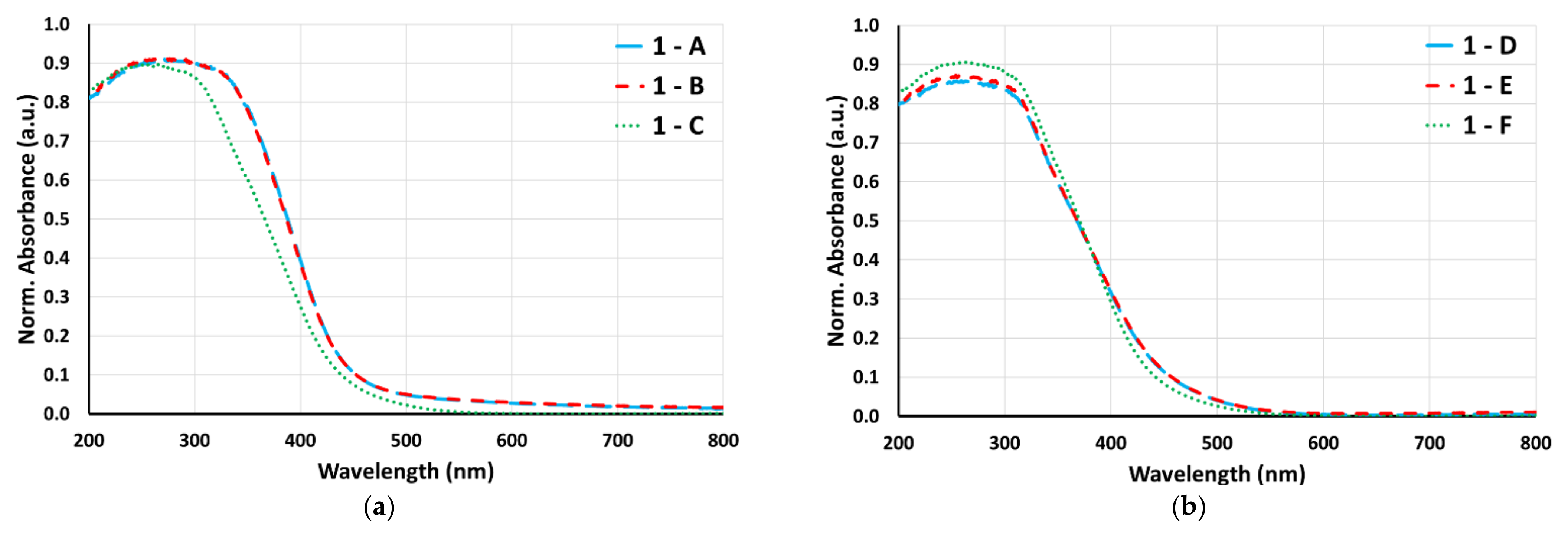
Figure 1 shows the solid-state DRS spectra of all the samples in Series 1 (MWA-HT-In2O3) calcined at 300 °C (Figure 1a), and 500 °C (Figure 1b). All the samples showed a preponderant light absorption in the near-UV range as expected for the In2O3. Of note is that samples 1A and 1B (prepared with 5 and 10 min heating ramp) showed overlapping spectra and differed from the spectrum of sample 1C (prepared with the 15 min heating ramp) (Figure 1a). The latter was narrower and showed a shift toward the blue, most likely due to the formation of defective and less crystalline particles induced by the prolonged nucleation time. The above features suggest that the preparation conditions (heating ramp duration and calcination temperature) affected the particle structure. Interestingly, the spectrum of the sample prepared at 300 °C with a longer heating ramp was more similar to those of the samples calcined at 500 °C.
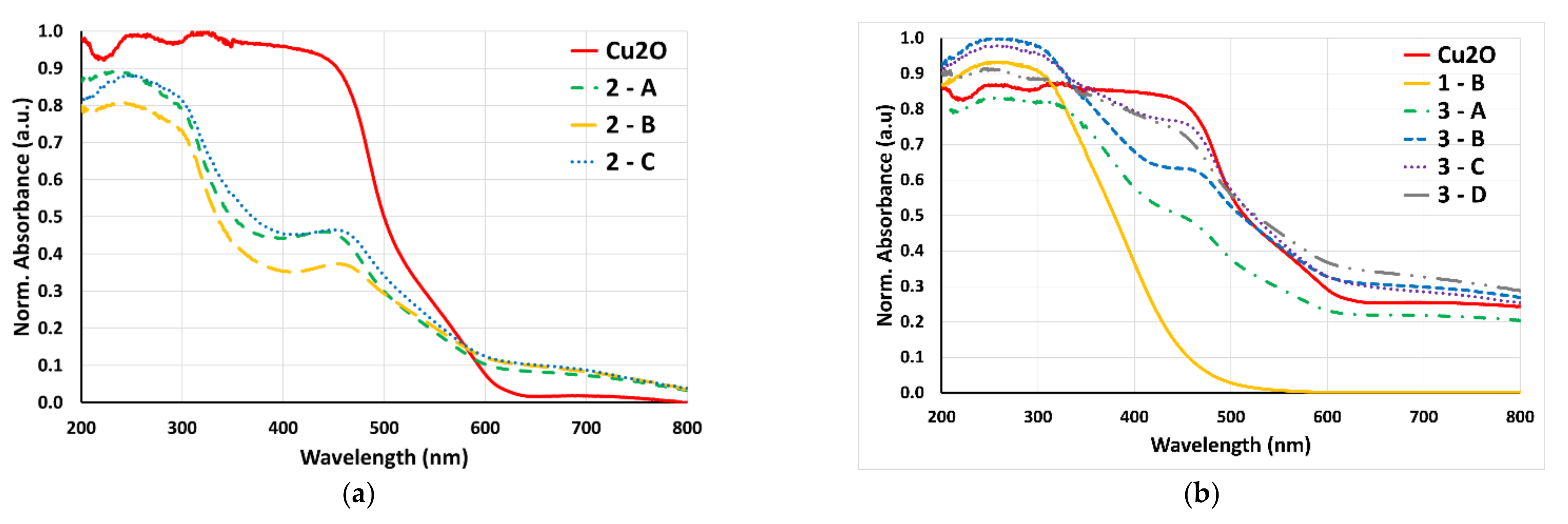
Figure 2 shows the UV-VIS solid state spectra for the samples of Series 2 (Cu2O-MWA-HT-In2O3), with variation in the MWA-HT treatment (Figure 2a), and those of Series 3 with a different Cu2O/In2O3 molar ratio (Figure 2b). Figure 2a shows that samples with similar composition and prepared in the same way showed the same spectral features, especially in the regions where peculiar fundamental absorption onsets emerged, as for the eminency of the binary oxide character. Particularly, the spectra largely differed from the bare Cu2O trace, thus, the very different contribution that the two partners offer to the absorption spectra of the composites are revealed; however, these arguments cannot be clearly assumed to unambiguously assign specific absorptions or optical energy gaps, because of the solid-state samples’ nature. Such differences are even more clearly observed in Figure 2b, where the change in materials’ composition, increasing the Cu2O/In2O3 molar ratio, resulted in a shift towards the visible region, with a spectrum shape that moved towards the bare Cu2O (red). The presence of absorption tails extending over 600 nm and with a higher intensity than for the Cu2O is considered indicative of larger particles and aggregates formation, mainly composed of Cu2O particles not interacting with the indium component and nucleating within the same species.
In both Series 2 and 3, the contribution of the Cu2O component revealed a shift from near-UV up to 600 nm [16]. Moreover, the spectra shown in Figure 2 qualitatively indicate that the two binary oxides were combined as the absorption onset was deeply modified with respect to the pure samples. Meanwhile, being out of a doping concentration regime, the single components continued to absorb radiation independently from each other. (Figure 2b)

2.1.1. Band-Gap Evaluation by UV-Visible Spectroscopy

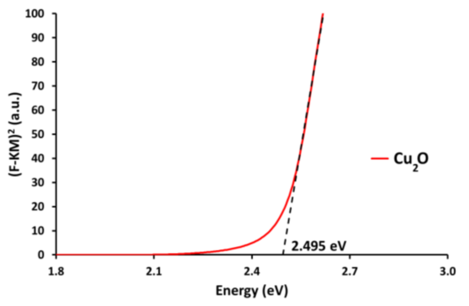
According to solid-state physics and semiconductor materials properties, the interaction with the radiation energy promotes one electron from the valence band to the conduction band, leaving behind a hole [18]. Generally, the first energy value matching with an electronic transition is known as an optical energy gap, Egopt, which can also differ from the lowest possible distance between the main VB and CB, i.e., the real electronic energy gap [19]. The Egopt is thus a fundamental property for these materials, especially when intended for applications in photocatalysis and photovoltaics [20,21]. It can be calculated from UV-visible spectroscopic data by using the Tauc Plot (TP) method [22]. In spite of its reliability, correctness, and appropriateness from both theoretical and experimental point of views that are under debate also for improvements and unification, TP is widely and commonly employed [23,24,25,26,27]. In the present work, the TP method was used to determine the Egopt based on the Kubelka–Munk function F(R), calculated from experimental reflectance spectra, and related to a form of linear absorption coefficient α, to the photon energy hν, and to the Egopt by means of a power law, the Tauc Equation:
F(R) · (hν) = A · (hν − Egopt)n,
where the exponent n describes the electronic transition type and the plot of F(R)·(hν) to the n−1 vs. hν shows a linear rise in the region of fundamental absorption. This part of the graph was fitted by a linear least square operation and the Egopt was extrapolated as the intersection of the fitted straight line with the energy axis [18,26,28]. This is reported in Figure 3 for the Cu2O component as a first example.
Unfortunately, such a procedure produces reliable results only when pure or slightly doped semiconductors are considered, where fundamental absorption edges are discernible and not for composites like those prepared in this work [18,26,28]. In order to gather some information, the TP was applied to the spectral features of single metal oxides in the composites, whose interaction was then quantified on the basis of experimental data (UV-Vis DRS and electrochemical properties). The linear regression fittings were optimized by maximizing the R2 correlation coefficient and requiring a minimum of 40 data points for statistical validation. Strictly following these criteria, extrapolation produced results with an error of the order of 1 meV, as listed in Table 1 together with an indication of the corresponding wavelength.
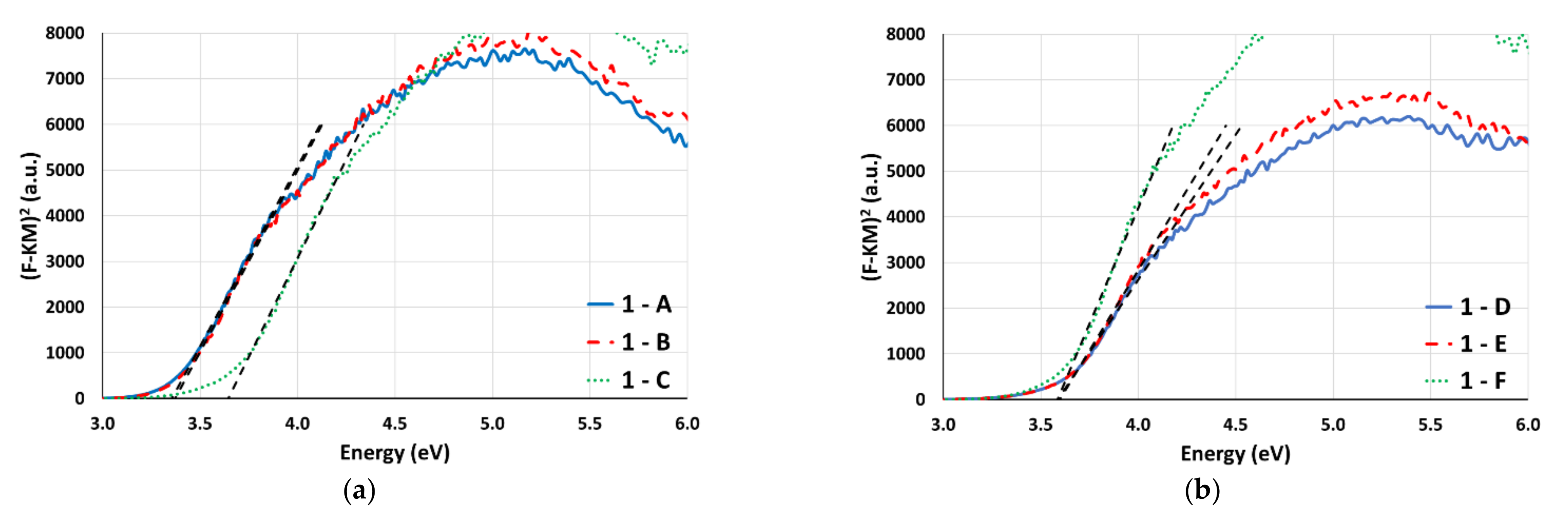
Data listed in Table 1 are extracted from plots in Figure 3 and Figure 4 where similarities between traces are evident and an extended linearity over which best fitting operation was executed. Some preliminary conclusions can be drawn from Figure 4 and Table 1. For both the Cu2O model and In2O3 samples, values were extracted considering that a direct allowed electronic transition occurs, thus n equals 0.5. It should be noted that this is correctly recognized for Cu2O, where the usual values are in the 1.8–2.2 eV range, but higher gaps can be observed for very small particles following a quantum confinement size effect, thus comprising the just determined value [8,29]. On the other hand, the same direct allowed electronic transition for the In2O3 can be justified only by considering recent studies among the plethora of studies about the controversial nature of the band structure and of the fundamental band gap, ranging from 2.6 to 2.9 eV [10,11,30]. This is clearly different from the measured values, but an effect due to preparation induced defects and vacancies can be invoked. Moreover, the optical gap should be considered as being derived from excitation of the first available electrons which are deeper in VB also at room temperature, a common feature for n-type conductive oxides such as In2O3 [11]. In the prepared samples, the higher (500 °C) calcination temperature resulted in a quite close but higher energy gap, and this was most likely due to the formation of equally defective particles. Conversely, when a lower (300 °C) calcination temperature was used, a lower optical gap value was observed for the samples prepared using the 5 and 10 min heating ramp, that were very similar, while the sample prepared using a 15 min heating ramp showed a higher value of the gap, closer to those observed for the samples calcined at a higher temperature, confirming what was found in the UV-Vis spectra (see §2.2). Such a difference was most likely due to the formation of less crystalline and more defective particles.

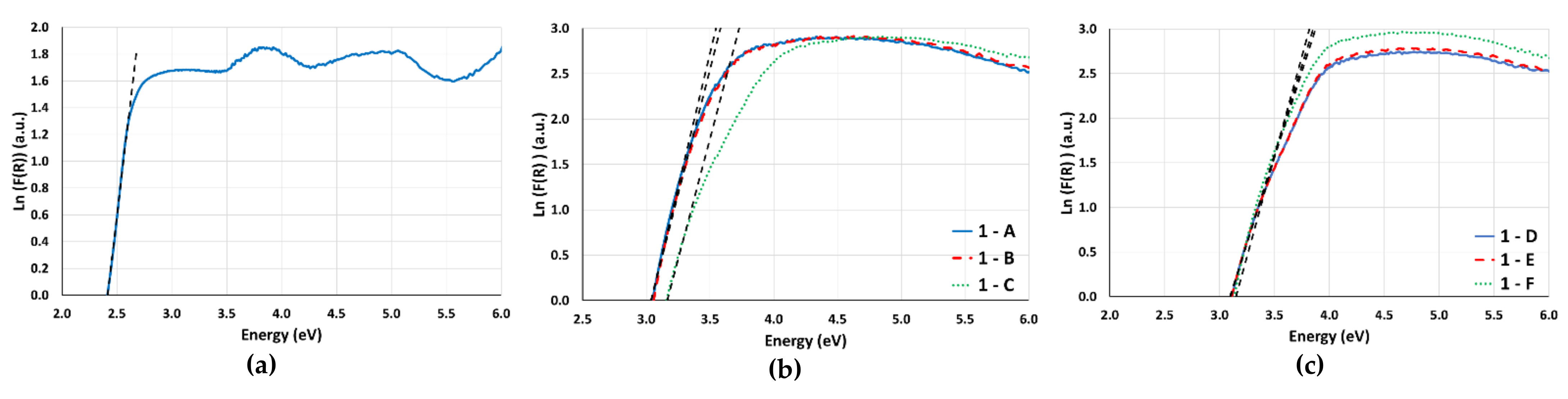
2.1.2. Urbach Tail by UV-Visible Spectroscopy

The graphs depicted in Figure 4 provide an indication about the optical energy gap of the ternary metal oxides, but the traces onset was not sharply rising in a defined point as happens in a pure metal oxide, which sometimes can be experimentally approximated by carefully deposed thin films. This mild absorption onset is somehow discernible also in the spectra in Figure 1 and it is called an Urbach Tail, related to particles’ size and size distribution, defects, crystallinity and presence of the amorphous phase [31]. The extension of these states in the energy spectrum can be modelled by Urbach energy, Eu [31,32], a scarcely reported parameter that we have determined here. The Eu determination requires linearization of the interested curved absorption tail, which is modelled with an exponential relation between the absorption coefficient α and the energy hν, as reported in Equation (2). The resulting linear region was fitted by linear least squares regression, whose slope is the reciprocal of the Eu parameter, and substituting to α the F(R) function:
ln F(R) = ln F(R)0 · (1/Eu) · hν,
For the determination of Eu, the fitting was performed maximizing the R2 correlation coefficient and with a computation over a minimum of 40 data points. Relative results, obtained after the graphs in Figure 5, are listed in Table 2, with the determination error ranges around less than 1.5% for all samples.
The fitting produced the lowest energy dispersion value in the Cu2O sample, and this represents a further confirmation of the adoption of a proper preparation method for this semiconductor, attaining a low size dispersion and high homogeneity of particles. In the case of the In2O3 samples, the application of different conditions during the hydrothermal treatment and calcination phase was reflected in two different series of results. In the samples of Series 1 with calcination at 300 °C, the Urbach energy was below 0.2 eV and linearly rose with the heating ramp duration (5 and 10 min), while in the samples of the same series calcined at 500 °C, the Urbach energy assumed higher values and lowered with the heating ramp duration. This suggests that an effective relation exists between the heating ramp duration, calcination temperature and their effects on semiconductor particles’ size and crystallinity, and thus the energetics. A higher calcination temperature produces more defective particles. Moreover, a longer heating ramp duration resulted in higher Eu, i.e., more defects. All the described features demonstrate that the preparation technique plays a crucial role in determining the opto-electronic properties of the photo-materials.

2.2. XPS Analysis

All binary metal oxides samples (Cu2O and MWA-HT-In2O3) and selected composites samples were measured by X-ray photoelectron spectroscopy (XPS) to determine the elemental composition and oxidation state with specificity in the samples’ surface, fundamental information for materials, and especially for semiconductors whatever the aimed application. This required a careful study of photoelectrons emission from specific core levels and Auger transitions in high resolution spectra. In particular, copper speciation was studied referring to high-resolution spectra of the Cu 2p3/2 core level (binding energy: 925–950 eV) and to Cu LMM Auger transition (BE: 555–600 eV), with consideration of the peak shape and result of the curve fitting operations [13,33,34,35]. Indium speciation involved the analysis of high-resolution spectra of the In 3d core level doublet (BE: 440–460 eV) and the InMNN Auger transition (BE: 1060–1090 eV) [13,35,36]. From the combined information derived by XP peaks and Auger transitions the following results were obtained: the presence of shake up features, albeit of low intensity, suggested that traces of Cu(II) were present; the main peak component was instead attributed to the Cu(I) state, thanks to BE and modified Auger parameter information. The Cu(I)/Cu(II) ratio was determined to be greater than 90/10, thanks to Cu 2p3/2 and O 1s core level curve fitting (Figure S1).
Similar arguments were adopted to study the indium speciation: the absence of plasmon loss feature, typical of metallic indium, led to conclude that the In(III)-oxide was the exclusive form found on the surface of every measured sample, as expected (Figure S2).
XPS analyses were also used to determine the surface elemental composition of the composites samples, i.e., ternary metal oxides in Series 2 and 3, and the results are listed in Table 3. The first set of samples in Table 3 refers to the composites described in Series 2 (Cu2O prepared in the presence of In2O3 with different MWA-HT conditions). Here, very similar Cu/In ratios were observed, as expected, demonstrating once again the reliability of the preparation method.
In the case of the Series 3, a not statistically relevant difference was observed in the composition among samples with a 1/1 molar ratio (3-A) and with a 10% (3-B) or 50% (3-C) excess. Moreover, there was not even a marked difference in composition of the lastly cited samples with the samples of Series 2, which were designed for analogous composition. Thus, the excess of the Cu2O component resulted in almost no effect on the surface composition, in agreement with the SEM images where a real coverage effect was not observed. On the other hand, the fourth sample of Series 3 showed a larger Cu/In ratio, thus following the expected rise in composition and demonstrating the effective enrichment in the p-component, despite that no structured composites were observed, i.e., defined particles’ surface functionalization.
As regards the copper and indium oxidation state, no marked variation was observed due to the procedure used to prepare the composites (Figures S3 and S4).

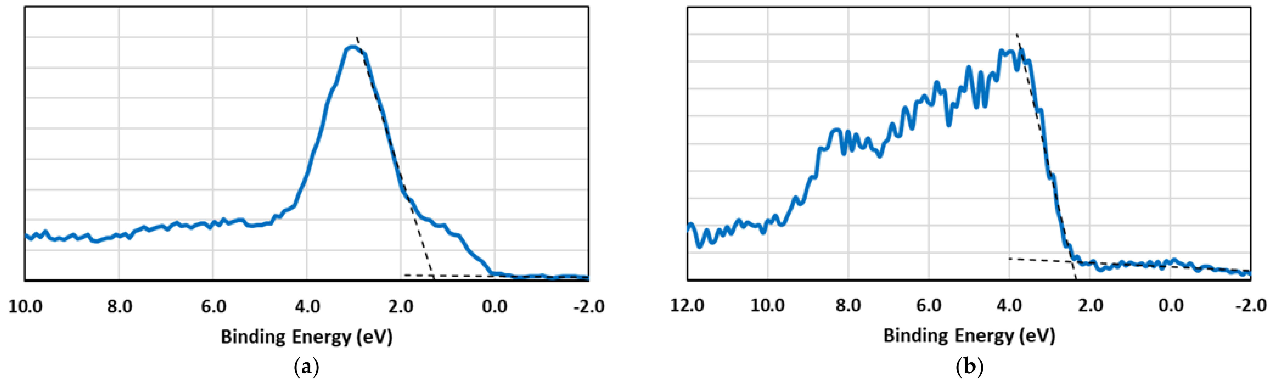
Valence Band Maximum Evaluation by XPS

Especially when a photocatalysis application is aimed, a fundamental step in semiconductive photo-materials characterization is the determination of electronic levels from which electrons, holes and radicals are transferred as reactive equivalents. Determination of these levels can be performed by adopting different experimental techniques and here we employed XPS. Because XP spectra are indicative of the density of bound states and of their electron population, the acquisition of the spectra in a narrow range around the Fermi energy of the system (BE 0) allows the determination of the populated valence band edge, usually corresponding to the valence band maximum or closely related. The measured BE range was −3–12 eV. Such an evaluation is based on a well-established, but not so common procedure, explained in detail elsewhere for covalent and not covalent materials [12,37,38,39]. It was here performed on the binary oxides samples [13]. Least square linear fittings were applied to the XP spectrum in the low BE region, producing a first straight-line accounting for spectrum background over the Fermi level. A second straight-line accounted for the leading edge, indicative of electron population. The intersection point of the two lines corresponded to the calculated VBM. In the present work, the least square fittings were optimized by maximization of both the R2 correlation coefficient and the included data points in the rising edge and considering all the available data points in the spectrum background region [13]. Figure 6 reports spectra for selected samples as examples of the described determination method. Table 4 accounts for the VBM extracted values for all the binary oxides samples for which the determination was performed. Every result was determined by measuring three spots of the same sample, and the error values were determined from the regression method extrapolation.
Figure 6a refers to the spectrum of the Cu2O, featuring a typical defined peaking signal, with a shoulder degrading to BE 0, which can be attributed to the interplay between the lowest energy electronic states and photoelectrons, also considering the easily changing copper oxidation state. Moreover, Figure 6b shows the spectrum for the second sample of Series 1 (10 min, 300 °C calc.), where a defined signal was observed, with no shoulders, and an extracted value falling at over 2.5 eV. Samples of the same series were analogously analyzed, and the relative spectra are reported in Figure S5, with the main difference in the plotted curves, which then were reflected in the extrapolated VBM values, being in the tailing effects in the rising edge portion of the graph.
XP spectra and valence band edge values for the In2O3 samples, differed with the preparation conditions and applied thermal treatment, confirming that the preparation procedure influences the photo-material properties. Particles’ size, size distribution, defects, and crystallinity, affect the opto-electronic properties and a rigorous protocol in the preparation of samples is necessary. Here, the sample with a longer heating ramp resulted in a higher VB value, suggesting the relevance of defects and crystallinity to a higher energy level (closer to 0 BE), or to a larger number of available electrons in the valence band.

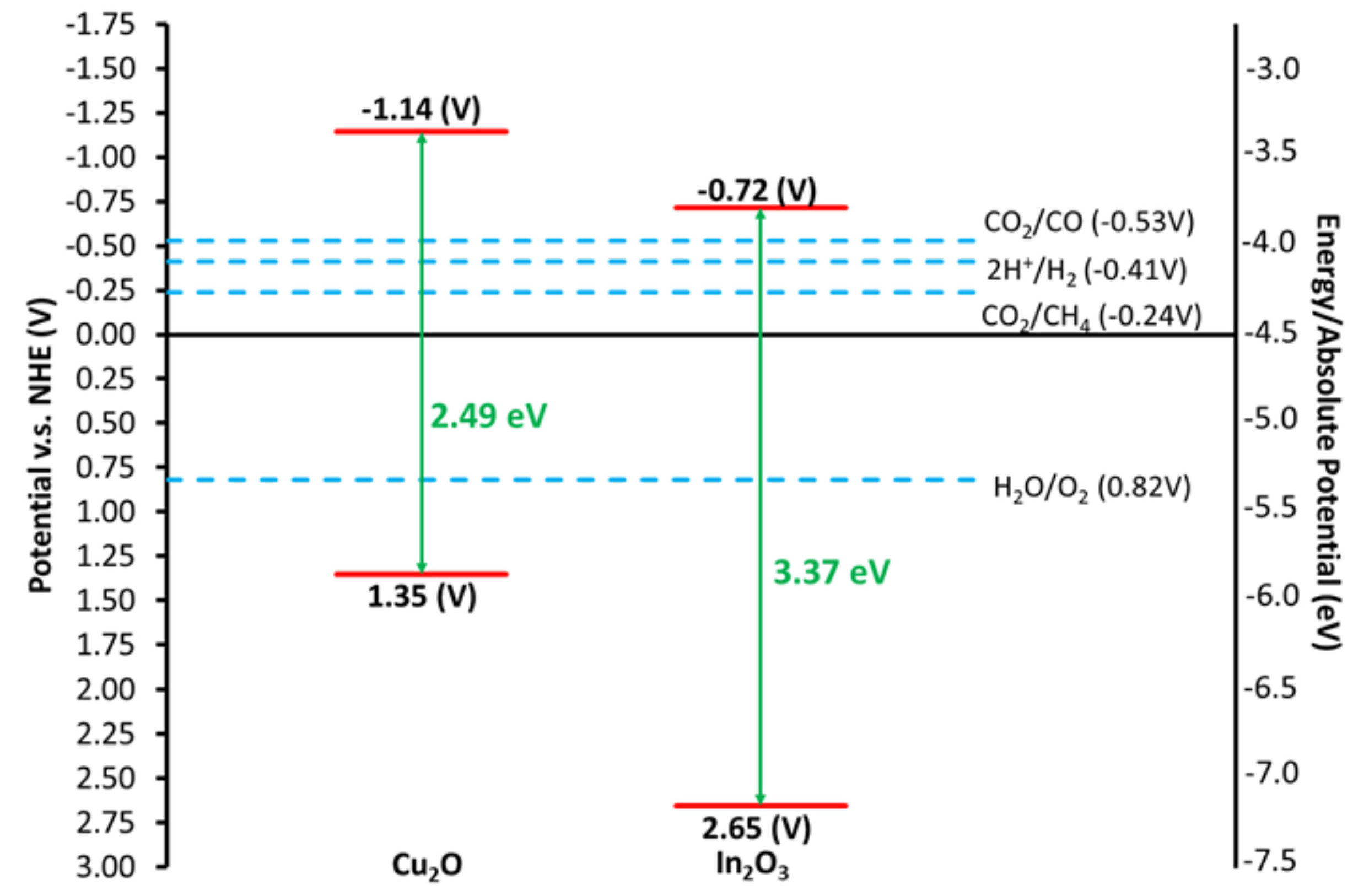
2.3. Band Structure Evaluation

Once the values for the optical energy gap and the valence band maximum were determined by the UV-visible DRS and XPS techniques, respectively, the extracted data were combined. This resulted in qualitative energy diagrams which correlated to the electronic band structures of the binary oxides. The same diagrams were directly composed for ternary oxides because it was not possible to accurately determine the nature and extent of the partners interaction in a direct experimental way [13]. Moreover, such a determination in the ternary oxides’ samples would lack sense because the comparable composition range and the intrinsic nature of the photomaterials’ composites caused the partners to absorb radiation independently, as previously shown, and to hide a clearly assigned VBM in the XPS determination.
It should be noted that this kind of scheme is commonly found in the literature to illustrate the photocatalytic reactions’ mechanism. Indeed, their determination by experimental/theoretical arguments always results in a difficult task, and even results in misleading conclusions [2,3,13]. An example of a diagram scheme determined in the present work is depicted in Figure 7. The structures for the Cu2O and the MWA-HT In2O3, prepared with a 10 min heating ramp and 300 °C calcination, are drawn next to each other.
In Figure 7, the determination is limited to a qualitative visualization and the possible partners interaction is not graphically highlighted because it was not clearly determined; however, the involved parent semiconductors are a p-type, Cu2O, and an n-type, In2O3 and an interaction coming from the formation of p,n-heterojunctions is highly sought after, after an energy level alignment. This would contribute to lowering the recombination rate of the charge carriers and to enhancing the possibilities of charge-transfer in photoreactions [12,13,15,40,41,42,43,44].
Figure 7 shows the levels involved in proton-coupled-electron-transfer (PCET) processes needed for CO2 reduction by coprocessing with H2O in a pure photocatalytic system. This is a difficult but, at the same time, very valuable process to be deployed to control CO2 emissions into the atmosphere by converting them into new fuels. Performing such a process using only solar light energy at ambient temperature is one of the target applications of such materials [1,2,3,13,45].
From the same Figure 7, it can be concluded that visible and UV radiation absorption can induce electrons to be promoted from VB to CB of both the partners, leaving behind electronic holes. Once photogenerated, these charge carriers could recombine on the same semiconductor where they have been generated or transferred from surface states to the reactant molecules. Conversely, the plausible interaction of energy levels between the two partners is a very valuable added feature, being able to prolong the charge carriers’ lifetime and raise possibilities for their effective use in some specific applications [2,3,13,46]. To some extent, such a positive effect could also occur in the case depicted in Figure 7. Here electrons from the CB of the Cu2O can move to the CB of the In2O3, and holes from the VB of the In2O3 can move to the VB of the Cu2O, but experimental proof of this can be attained only by a direct test of the photo-materials’ opto-electronic properties.

2.4. Photoinduced Transient Current

After qualitative determination of the electronic band structure levels, the final step in the characterization of the semiconductor photo-materials was the determination of their opto-electronic behavior. Electrochemical measurements in the potentiostatic regime in a three-electrode glass cell confirmed the insurgence or not of photogenerated charge carriers (electrons and holes), eventually stabilized by a partners’ interaction, and ready to be used [47,48,49]. The current between the ITO/glass photoelectrode covered with the photo-material under evaluation (working electrode) and a Pt foil counter electrode (with respect to a reference electrode) was measured, after the open-circuit-potential was applied to the cell. The photoinduced current was measured after the absorption of radiation from a white LED lamp in a sequence of on/off cycles.
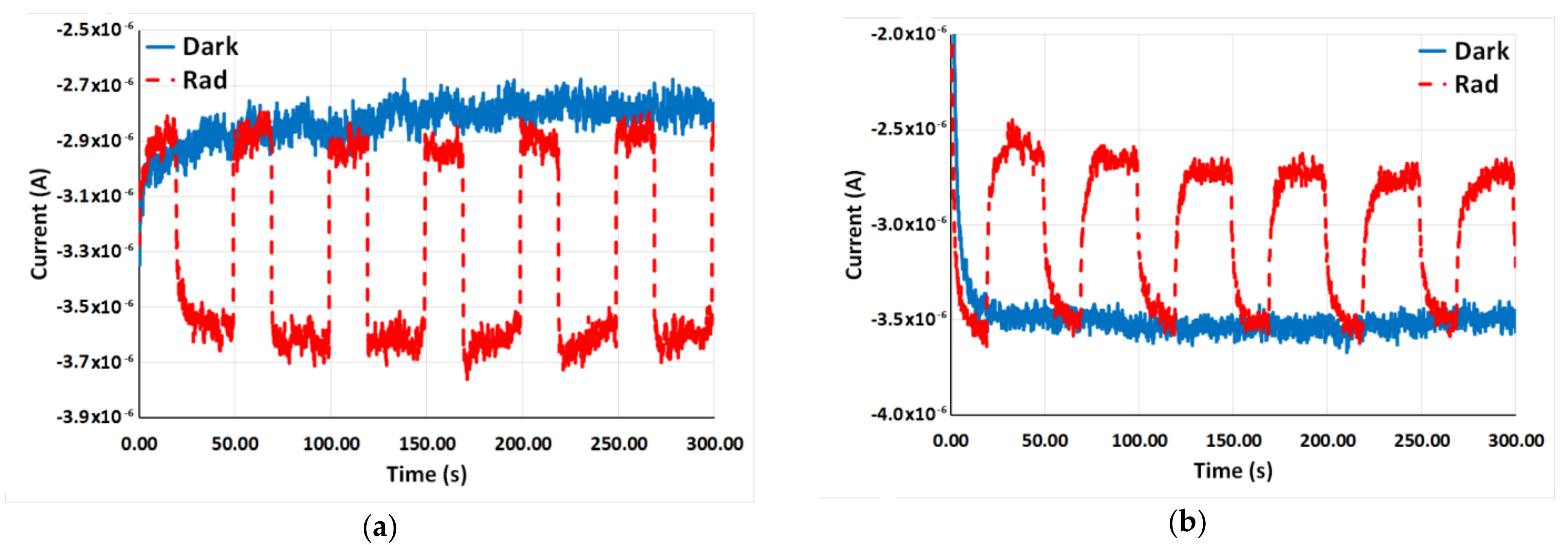
Parent oxides of the Cu2O and In2O3 were measured first, where the latter was prepared by MWA-HT procedure with a 10 min heating ramp duration and 300 °C calcination. Current vs. time curves under cyclic irradiation are depicted in Figure 8.
The blue solid trace refers to a dark condition, which resulted in a quite flat constant curve. The dashed red trace refers to the irradiation condition, which resulted in square-like peaks. Such notation is the same for all the other analogous graphs. The contribution of the semiconductor photo-material deposition on the measured currents is clear. In both samples the current strictly followed the on/off cycling of the irradiation and the induced current was in the μA range, two magnitudes larger than the 10−8 A observed in the bare not functionalized ITO/Glass photoelectrode, and in the typical magnitude observed for this kind of photoelectrode. This observation led to the conclusion that the parent photo-materials were able to generate charge carriers after radiation absorption and that these were available to be transferred in photocatalytic processes where they played the reactant/initiators role. Noteworthy, thanks to the potentiostat settings for the current sign, was that it was possible to discern whether the induced current was anodic (upward peak) or cathodic (downward peak), thus, determining the semiconductor type of the photo-material. Therefore, while the Cu2O sample produced downward peaks, correctly corresponding to the expected p-type character, the In2O3 sample produced upward peaks, correctly corresponding to the expected n-type character. Such a feature result was useful to also evaluate the semiconductor type in the composites samples depending on the concentration contribution.
The composites of Series 2 were employed to fabricate relative photoelectrodes which were measured as above. The resulting current vs. time curves in cycled irradiation conditions are reported in Figure 9. Anodic photocurrents of tens μA were observed for the samples containing In2O3 prepared with a 5 or 10 min heating ramp, Figure 9a,b respectively. The curve relevant to the composite containing the In2O3 prepared with a 15 min heating ramp showed currents lower than 10 μA. (Figure 9c) Such a trend is associated with the observed different optical energy gap, confirming the strict relation between the preparation protocol and the properties of the materials. On the other hand, the latter sample showed a less marked decay during the irradiation peak compared to the two other samples of the series. This was ascribed to the charge carriers’ stabilization and to a somehow enhanced interaction between the partners.
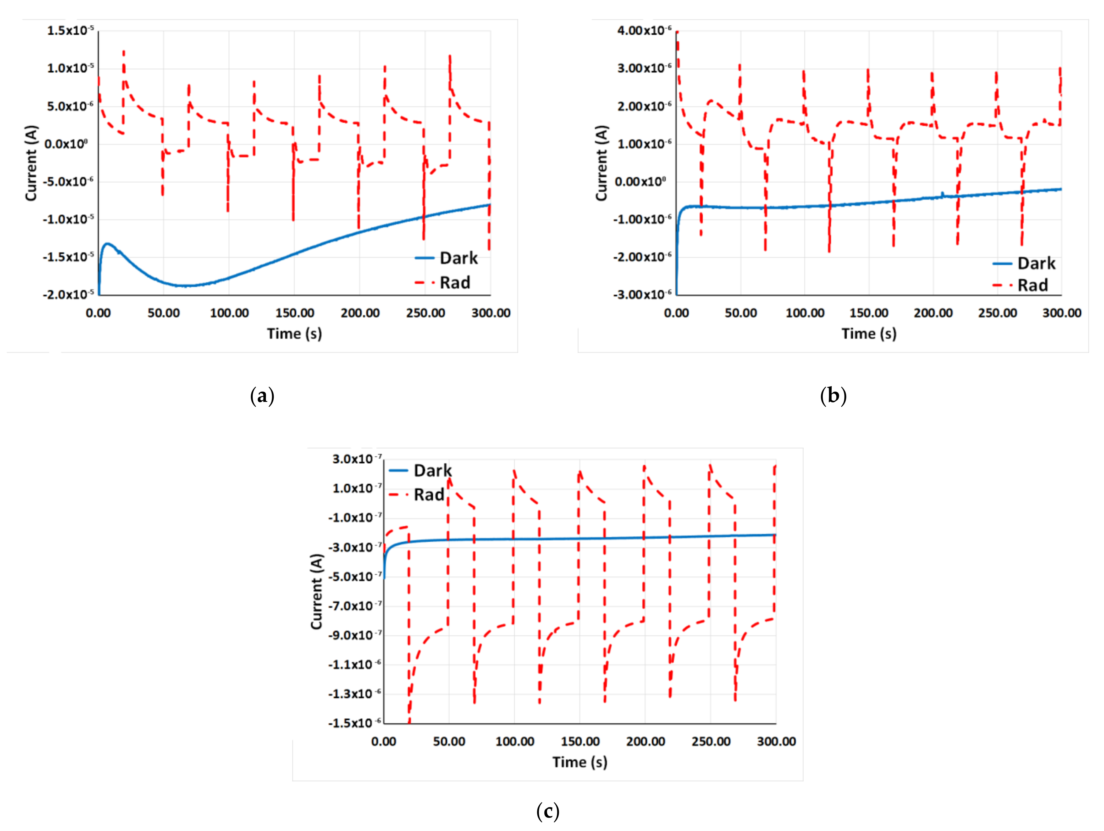
Finally, Figure 10 reports the current vs. time curves for composites described in Series 3, with a progression in the Cu2O/In2O3 molar ratio. The 10% Cu2O-excess (3-B) (with respect to a 1:1 molar ratio) in Figure 10a resulted in currents on the half μA range, with pronounced peaks featuring when the light pulse started and ended, typically observed in the composites containing Cu2O. This can be considered specific of such material, and due to its characteristic high charge recombination rate, which was also discernible in the quick decay during the absorption pulse. This contribution was even more evident in Figure 10b, referring to the 50% excess in composition. Currents were in the μA range and denoted a higher recombination rate and lower conduction. The peaking part when the irradiation pulse started and ended was more evident and had the direction of a p-type semiconductor (downwards). The current level results somehow stabilized with a lower decay during the irradiation pulse.
Finally, in the Cu2O/In2O3 sample with a molar ratio 2/1, (Figure 10c) the cathodic-type current, due to the large amount of Cu2O, was in the μA range and the peaking behavior at start and end of the light pulse was again quite marked. A higher stabilization was observed, as shown by the reduced decay during the light pulse.

2.5. Comparison of Cu2O@In2O3 vs. Cu2O-In2O3@TiO2

Copper oxides are widely recognized as very interesting p-type semiconductors because of their enhanced light absorption in the visible range, but their high charge recombination rate represents a major drawback for their utilization as photo-materials in various application fields [7,8]. This is the reason why, whatever the intended use, the formation of p,n-heterojunction systems is considered a smart strategy to improve copper oxides’ properties and taking the best from them and from their combination with n-type partners [43,44,46]. As for photocatalytic application, the latter are mainly implied in performing oxidation reactions [50,51,52,53], and the efficient combination of electronic levels with those of a p-partner, can result in charge separation and stabilization.
To improve the n-partner In2O3‘s role in the semiconductor material, we decided to combine the ternary Cu-In oxide with titanium oxide, TiO2, widely used in photocatalytic oxidation of pollutants both in air and water systems [50,51,52,53]. Inspired by recent literature studies [54,55,56], TiO2 was used as support for the Cu@In photo-materials, and composites were prepared (see Materials and Methods Section), where TiO2 was the main component and Cu(I) and In(III) oxides were added in low amounts, so as to dope the TiO2. In order to evaluate the contribution of the TiO2 component, a characterization phase, analogous to that performed for other samples, was applied to the quaternary oxide. Bare TiO2 and Cu2O-In2O3@TiO2 were compared for their UV-visible DRS spectra, with the optical energy gap determined by Tauc plot, and valence band maximum determination by XPS and photoinduced transient photocurrent. (
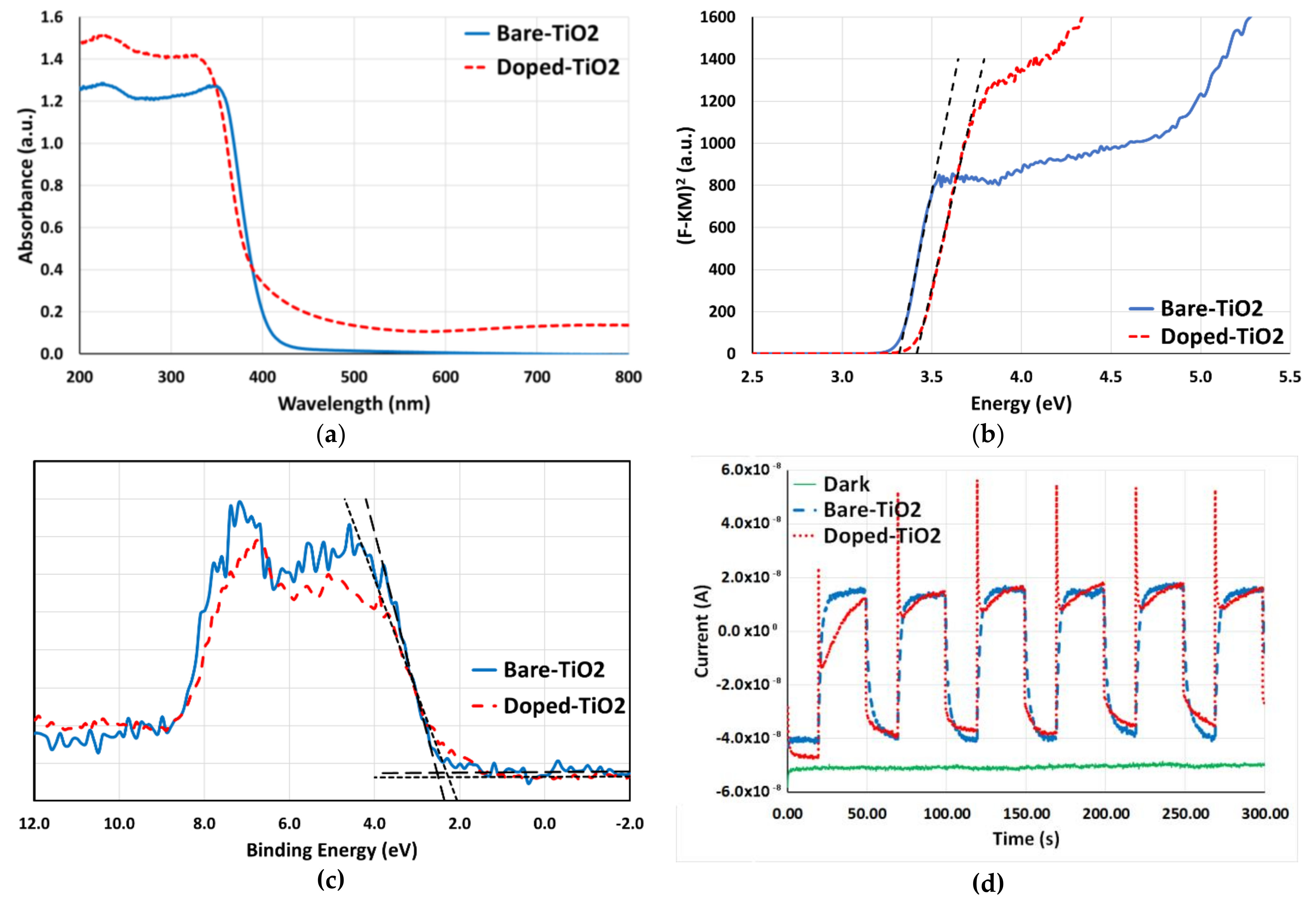
Figure 11).
The same samples were measured by XPS for surface composition/determination (Figure S6). It should be noted that the surface Ti was always in the solely TiO2 form, and the In and Cu components resulted in the solely Cu2O and In2O3 form. Moreover, the determination of the surface composition of the quaternary oxide showed up a value of 0.53 ± 0.31 for the Cu/In ratio and a total of 0.03 ± 0.01 for the (Cu + In)/Ti ratio, as confirmation of the doping concentration regime and of the very little amount of the Cu component.
From the DRS absorption spectra depicted in Figure 11a, the doped sample resulted in a generally larger absorption, but both the samples had a main absorption in the UV range, where the optical energy gaps fell. Doping the TiO2 with Cu and In oxides moved the gap to higher energies, due to the additional contribution of the In2O3 component.
Optical energy gaps were determined assuming that a direct allowed electronic transition occurred, and Figure 11b reports the relative Tauc plots. The gaps for the two samples barely differed for about 0.1 eV, with the bare-TiO2 showing an extracted gap of 3.32 ± 0.01 eV to be compared to the 3.42 ± 0.02 eV gap of the Cu2O-In2O3@TiO2 sample. Even the larger optical energy gap of the Cu2O-In2O3@TiO2 sample with respect to the TiO2 was ascribed to the contribution of the In2O3 component.
The VBM were extrapolated from the relative XP spectra reported in Figure 11c, where the traces appear to be quite overlapping. A more mindful observation led us to conclude that the doped sample was characterized by a larger number of available states and electrons over the determined VB edge (from the spectrum onset). This could have highly contributed to offer states from which the charge carriers could be transferred in the photoreaction. The extracted VBM was equal to 2.53 ± 0.06 eV and 2.32 ± 0.05 eV, for the bare and doped TiO2 samples, respectively.
Despite the applied calcination treatment (see Materials and Methods Section), XPS determination of the oxidation state showed that the copper oxide present at the surface of the composite was in the form of Cu2O (Figure S6). Thus, the electronic band structure scheme derived in Figure 7 can still be applied, even though the dopant components were added by a different preparation procedure. Some differences do clearly emerge in Figure 12. Of note is that compared to the scheme with no-TiO2 component, the levels for this third oxide (from the bare sample) were set between those of the two other oxides. This could have highly contributed to the photoreaction result not only by providing useful levels for the charge transfer processes, but especially by enhancing a charge separation and, therefore, suppressing/lowering the charge carriers recombination. Once the plausible band structure scheme was plotted, the opto-electronic characterization of the TiO2 containing composites was concluded with the measurement of the transient photoinduced currents.
The relative traces in Figure 11d show that the photo-materials strictly followed the irradiation cycles with perfectly overlapping behavior, thus no contribution to the radiation absorption could be directly invoked for the photocatalytic performances. Of note is that while the binary and ternary oxides discussed above did show currents up to 10−6 A or even 10−5 A, the binary (dashed blue trace) or quaternary (dotted red trace) oxides containing the TiO2 component showed currents in the 10−8 A range. Such a two-three orders of magnitude difference indicates a low efficiency for light absorption. This can be explained considering that: (i) the irradiation was performed with white light with only 5% UV-radiation, (ii) the materials containing the TiO2 were UV absorbers, and (iii) the In2O3 materials showed a not negligible absorption tail over 400 nm (see Figure 1). At the same time, samples with a doped TiO2 component showed a less than sharp decay after the irradiation in the off phase, indicating that some sort of stabilization and separation of the charge carriers did effectively occur.
As already discussed, this further supports the fact that the photo-materials’ properties, such as the optical energy gap and band edge levels, are not the only factors responsible for their activity as photocatalysts. The effects of combination on the behavior of the charge carriers and on stabilization must be taken into deep consideration. The matching of levels and transfers must also be investigated with an interplay of different techniques.

2.6. SEM of Ternary and Quaternary Oxides

Figure 13 shows the SEM images of the Cu2O-In2O3 and Cu2O-In2O3@TiO2 materials and some differences emerge with comparison of the two images. Cu2O and In2O3 (1B) are sub-micrometer particles, as it is shown in the SEM images and related EDS spectra in the supporting materials (Figure S7).
In particular, the Cu2O particles were in the form of aggregated spheres with about a 50 nm diameter. This is a common shape for this specific material. The In2O3 particles were in the form of nanorods more than 200 nm long. They look multifaceted as if they were composed of smaller rods. Mixed ternary or quaternary oxides are composites structures and Figure 13a features the Cu2O-In2O3 composite where particles of the two oxides were in contact and aggregates were formed in the 1/1 molar ratio sample. The presence of In2O3 nanorods appeared to induce further Cu2O particle growth, with a diameter of more than 200 nm in some cases. The relative EDS spectrum is reported in Figure 13b and it shows the sole presence of Cu, In and O atoms. Cu2O and In2O3 particles produced sub-micrometer composites with p,n-junctions while the Cu2O did not give a uniform coverage of the In2O3 particles.
Aggregates of the nanometric Cu2O and In2O3 are supposed to exist on the micrometric-TiO2 phase that acts as a host in a doped system (Figure 13c). The associated EDS spectrum is reported in Figure 13d, showing the large amount of Ti atoms, with TiO2 being the major component, and the presence of Cu and In atoms in dopant concentration.
All such features agree with the opto-electronic data discussed in the paragraphs above.

3. Materials and Methods

The following reagents were used as received and without any further treatment: anhydrous CuSO4 (BDH Chemicals ltd, Poole, England), Cu(NO3)2xH2O (Sigma-Aldrich, Steinheim, Germany), In(NO3)3xH2O (Sigma-Aldrich, Steinheim, Germany), Titanium (IV) isopropoxide (Sigma-Aldrich, Steinheim, Germany), Urea (Sigma-Aldrich, Steinheim, Germany), NaOH pellets (Fluka AG in Sigma Aldrich, Steinheim, Germany), L-Ascorbic Acid (Alfa Aesar, GmbH, Karlsruhe, Germany), NH4OH (30% v/v, Carlo Erba Analyticals srl, Milano, Italy), KCl (Sigma-Aldrich, Steinheim, Germany), 2-propanol (Sigma-Aldrich, Steinheim, Germany). Deionized Water was used for all syntheses in which a solvent was required.

3.1. Preparation of Oxides

Single metal oxide samples were prepared by two different techniques: (i) microwave assisted hydrothermal treatment (MWA-HT) for In2O3; and (ii) in situ chemical reduction of lab-made Cu(OH)2 in an aqueous solution for Cu2O. If not differently indicated, all operations were performed at ambient temperature and in the air.

3.1.1. Stable Cu(OH)2

Stable Copper (II) hydroxide samples were prepared by dropwise adding 4 mL of a concentrated NH4OH commercial solution (30% v/v) into 20 mL of a 0.5 M CuSO4 aqueous solution. The addition resulted in a dark blue clear solution, containing the hydroxide of the ion complex tetra-amino-di-aquo-Cu(II), [Cu(NH3)4(H2O)2]2+. Afterwards, 40 mL of a 0.5 M NaOH aqueous solution was dropwise added, under constant stirring, to produce a light blue suspension of Cu(OH)2 flakes, clearly observable. Immediately, the suspension was filtered on filter paper by a Buchner funnel, to eliminate as much water as possible and avoid conversion into copper (II) oxide and washed with deionized water. The filter paper was allowed to naturally dry in air under a fume hood for 4 h. At the end of the process a light blue solid was obtained in the form of very brittle scraps; the powder material was stored with no inert atmosphere protection.

3.1.2. Cu2O

Copper(I) oxide samples were prepared by dispersing the adequate amount (0.68 g) of Cu(OH)2 powder in 20 mL of deionized water under stirring. To this dispersion, 40 mL of a L-ascorbic acid aqueous solution (0.18 M)) was added dropwise under constant stirring and room temperature. The dispersion underwent color changes from light blue to light green to yellow to orange with the addition of the reductant solution.
At the end of the addition, the solution was immediately transferred to glass bottles for centrifugation and washing. Four steps, each followed by careful elimination of the supernatant liquid phase and addition of further deionized water, were carried out. At the end of the washing the wet residuals were vacuum dried for 4 h at ambient temperature. The dried materials were easily collected by grinding the very fine dark orange powder.

3.1.3. In2O3

For In(III) oxide preparation, 0.85 g of In(NO3)3·H2O was dissolved in 30 mL of deionized water to prepare a 0.01 M solution. To such solution urea powder (0.90 g) was slowly added so that a 1/5 molar ratio between the precursor salt and urea, which acted as a slow-reacting base, was attained.
The solution was kept at room temperature under constant stirring for 30 min, then it was transferred to a PTFE vessel for microwave assisted hydrothermal treatment (MWA-HT) by means of the Microwave Digestion System Start E (Milestone, FKV, Torre Boldone, Bergamo, Italy). Every vessel was filled with a 30 mL batch solution and was kept under constant stirring during the hydrothermal process. The system was heated from room temperature up to 120 °C by application of a different heating ramp duration (5, 10, and 15 min) and kept at the final temperature for 2 h. At the end of the planned time, the vessels were allowed to cool down naturally.
The content of the vessels, a milky white dispersion, was then transferred to glass bottles with the aid of further deionized water and separated by centrifugation. Five steps each were followed by careful elimination of the supernatant liquid phase with the addition of further deionized water for washing the material being carried out. At the end of the washing phase, the wet residues were vacuum dried for 2 h; afterwards the materials were easily collected by grinding a very fine white powder, In(OH)3. Finally, the powders were calcined in static air for 2 h at 300 or 500 °C, so that the precursor hydroxide was converted into In2O3.
By using this method, 6 samples labelled as 1-A (5 min, 300 °C), 1-B (10 min, 300 °C) 1-C (15 min, 300 °C), 1-D (5 min, 500 °C), 1-E(10 min, 500 °C), and 1-F (15 min, 500 °C) were prepared.

3.1.4. Preparation of Mixed Oxides

Mixed oxides were prepared by replication of an in-situ chemical reduction of the Cu(OH)2 to form Cu2O in the presence of adequate amounts of already prepared In2O3 powder. This two-step procedure for Cu2O preparation allowed for the weighting of the required masses for the direct precursors, so that composition mistakes due to the presence of many species and equilibriums in solution were avoided.
An amount of 0.25 g of Cu(OH)2 and 0.20 g of In2O3 powders required in the synthesis of the planned sample were dispersed in 20 mL of deionized water and kept under constant stirring at room temperature. Then, 40 mL of a L-ascorbic acid aqueous solution were dropwise added to cause the reductant agent to react with the Cu(OH)2 in a 1:1 molar ratio. The dispersion followed color changes from light blue to light green to yellow to orange with the addition of the reductant solution as in the case of pure Cu2O. The solution followed the same procedure described for pure Cu2O.
Two series of samples were prepared: (i) Series 2 where the samples were labelled as 2-A (5 min, 300 °C), 2-B (10 min, 300 °C) and 2-C (15 min, 300 °C) and (ii) Series 3 labelled as 3-A (10 min, 300 °C-1/1), 3-B (10 min, 300 °C-1/1 + 10%), 3-C (10 min, 300 °C-1/1 + 50%), and 3-D (10 min, 300 °C-2/1) varying also the Cu2O/In2O3 molar ratio.

3.1.5. Preparation of TiO2 and Its Composites

An amount of 10 mL of stock titanium-tetra-isopropoxide was added to 30 mL of 2-propanol under constant vigorous stirring at room temperature. After 30 min, the dropwise addition of 7 mL 1 M aqueous solution of acetic acid (added with 10 mL 2-propanol) was used to perform acid hydrolysis. The produced solution was aged at room temperature for 24 h under constant stirring.
The solution was then completely dried in an air oven at 80 °C, and the produced powder was calcined in air at 500 °C for 5 h.
For preparation of the doped TiO2 sample, after the 24 h aging, 15 mL of a 2-propanol solution containing the proper amount of precursor salts (nitrate) of doping metals was added at room temperature. The sol was aged for a further 12 h and then completely dried in air oven at 80 °C. The same calcination temperature was finally applied.

3.2. Characterization

Powder materials composition was determined by EDX measurements using an EDX-720 Shimadzu Spectrometer (Shimadzu Europe, Duisburg Germany).
UV-visible DRS spectra were recorded in the 200–800 nm region using a Cary-5000 spectrophotometer (Agilent Technologies, Santa Clara, California, USA), equipped with an integration sphere covered by a polymer internal coating, with a standard sample of the same material and with a sample-holder for the powder material.
X-ray photoelectron spectroscopy (XPS) analyses were run on a PHI 5000 Versa Probe II Scanning XPS Microprobe spectrometer (ULVAC-PHI Inc., Kanagawa, Japan). The measurements were completed with a monochromatised Al Kα source (X-ray spot 200 μm), at a power of 50.3 W. Wide scans and detailed spectra were acquired in the fixed analyzer transmission (FAT) mode with a pass energy of 117.40 eV and 29.35 eV, respectively. An electron gun was used for the charge compensation (1.0 V 20.0 μA). Data processing was performed by using the MultiPak software v. 9.9.0.8.
The transient current induced by radiation absorption in the photomaterials was measured using a 3-electrode glass cell where a 0.1 M KCl aqueous solution was the electrolyte. The system was run by a Potentiostat (1230B, CH Instruments, Austin, Texas, USA) using a laboratory made Ag/AgCl/KCl sat. electrode as the reference, a Pt foil as the counter electrode and an ITO/Glass slice as the working electrode. The working electrodes were fabricated by dropping photomaterial powders dispersed in 2-propanol and allowing the dispersant to evaporate in air at room temperature. The irradiation source for the transient current measurement was provided by an Osram White LED Lamp (P PAR 16 80 36°, 6.9 W/840 GU10), recording the current between the Counter and Working electrodes over time in many repetitions after measuring the open circuit potential and applying it to the cell in a static condition. A home-made assembled electronic driver was used to pilot the LED lamp and alternate the on/off radiation cycles.
Field emission scanning electron microscopy (FE-SEM) was performed by using a Zeiss Sigma Microscope (Carl Zeiss Co., Oberkochen, Germany) operating in the range 0.5–20 kV and equipped with an in-lens secondary electron detector and an INCA energy dispersive spectroscopy (EDS) detector. FE-SEM samples were prepared by casting a few drops of the nanoparticles suspension in ethanol onto a silicon slide. The samples were mounted onto a stainless-steel sample holder by using double sided carbon tape and grounded by silver paste.

4. Conclusions

In the present work, we have described the synthesis and characterization of mixed metal oxides such as p,n-junction, and have demonstrated that a correlation between the preparation technique and opto-electronic properties of the materials exists. A rigorous protocol is necessary for the synthesis of potential photocatalysts, which may significantly change their properties upon varying, for example, the rate of heating during calcination.
Solid-state UV-visible, diffuse reflectance spectroscopy (UV-VIS DRS) allowed for the determination of the light absorption properties and the optical energy gap. X-ray photoelectron spectroscopy (XPS) allowed for the determination of surface speciation and composition and for the determination of the valence band edge. The opto-electronic behavior was evaluated measuring the photocurrent generated after the absorption of chopped visible light in a 3-electrode cell. Scanning electron microscopy (SEM) measurements allowed for the auxiliary characterization of size and morphology showing the interaction existing among the p,n-component oxides. SEM images have shown that binary oxides particles are associated in ternary oxides and that quaternary oxide samples present host TiO2 doped with Cu2O-In2O3.
Opto-electronic characterization of the composites resulted in reliable results and the correlation of the opto-electronic properties with the preparation method was clearly established. Mindful combination with the XP results has allowed for the determination of electronic band structure schemes. Ternary oxides showed a dependence of light absorption and photocurrent from the composition, with the Cu2O component fully exploiting its p-type character. The characterization of the quaternary mixed oxide, containing TiO2, Cu2O and In2O3, confirmed that the material was, as planned, a host TiO2 doped with Cu2O and In2O3 with properties modified with respect to the bare host material. In all cases, a strong dependence of the properties of the materials from the synthetic methodology was ascertained, calling for rigid protocols in manufacturing semiconductors.

Supplementary Materials

The following supporting information can be downloaded at: https://www.mdpi.com/article/10.3390/catal12020153/s1, Figure S1. (a) Cu 2p3/2 XPS peak and (b) XAES CuLMM peak for the Cu2O sample, with determination of Cu(I)/Cu(II) ratio and corrected Auger parameter; peaks features are highlighted; Figure S2. (a) In 3d doublet XPS peak and (b) XAES InMNN peak for the In2O3 sample, with determination of corrected Auger parameter; peaks features are highlighted; Figure S3. Cu 2p3/2 XPS peak for the samples in Series 2, accounting for variation of In2O3 prepa-ration conditions in respect of analogous Cu2O/In2O3 molar ratio; corrected Auger parameter is indicated; Figure S4. (a) Cu 2p3/2 XPS peak for the samples in Series 3, accounting for variation of Cu2O/In2O3 molar ratio, and (b) table for indication of Cu(I)/Cu(II) atomic percentages ratio in the samples; Figure S5. XP Valence Band Spectra in In2O3 samples prepared by MWA-HT procedure in Series 1: (a) 1-A, (b) 1-C and (c) 1-E; Figure S6. (a) Cu 2p3/2 XPS peak and (b) Ti 2p doublet XPS peak for the Cu2O-In2O3@TiO2 sample; Figure S7. SEM image of (a) Cu2O particles and (b) relative EDS spectrum; SEM image of (c) In2O3 (sample 1-B) particles and (d) EDS spectrum. The reported size scale indication is 200 nm long.

Author Contributions

Conceptualization, M.A. and A.D.; methodology, M.A. and A.D.; validation, M.A., A.D. and F.N.; XPS analysis, N.D.; SEM Analysis, R.C.; investigation, D.M.S.M.; resources, A.D.; data curation, F.N.; writing—original draft preparation, D.M.S.M.; writing—review and editing, M.A. and D.M.S.M.; supervision, A.D.; project administration, A.D.; funding acquisition, A.D. All authors have read and agreed to the published version of the manuscript.

Funding

This research was funded by MIUR (PRIN Project “CO2 only”-2017WR2LRS and PON R&I 2014-2020 -ARS01_00868).

Data Availability Statement

Not applicable.

Acknowledgments

IC2R is acknowledged for making available some equipment and scientific-technical assistance.

Conflicts of Interest

The authors declare no conflict of interest.

References

  1. Marcolongo, D.M.S.; Aresta, M.; Dibenedetto, A.; Aresta, M. Stepping toward the Carbon Circular Economy (CCE): Integration of Solar Chemistry and Biosystems for an Effective CO2 Conversion into Added Value Chemicals and Fuels. In Advances in Inorganic Chemistry; van Eldik, R., Hubbard, C., Eds.; Elsevier: Amsterdam, The Netherlands, 2021; pp. 289–351. [Google Scholar]
  2. Habisreutinger, S.N.; Schmidt-Mende, L.; Stolarczyk, J.K. Photocatalytic reduction of CO2 on TiO2 and other semiconductors. Angew. Chem.-Int. Ed. 2013, 52, 7372–7408. [Google Scholar] [CrossRef] [PubMed]
  3. Nikokavoura, A.; Trapalis, C. Alternative photocatalysts to TiO2 for the photocatalytic reduction of CO2. Appl. Surf. Sci. 2017, 391, 149–174. [Google Scholar] [CrossRef]
  4. Tong, H.; Ouyang, S.; Bi, Y.; Umezawa, N.; Oshikiri, M.; Ye, J. Nano-photocatalytic Materials: Possibilities and Challenges. Adv. Mater. 2012, 24, 229–251. [Google Scholar] [CrossRef]
  5. Chavali, M.S.; Nikolova, M.P. Metal oxide nanoparticles and their applications in nanotechnology. SN Appl. Sci. 2019, 1, 607. [Google Scholar] [CrossRef] [Green Version]
  6. Bagal, I.V.; Chodankar, N.R.; Hassan, M.A.; Waseem, A.; Johar, M.A.; Kim, D.H.; Ryu, S.W. Cu2O as an emerging photocathode for solar water splitting—A status review. Int. J. Hydrogen Energy 2019, 44, 21351–21378. [Google Scholar] [CrossRef]
  7. Zhang, N.; Sun, J.; Gong, H. Transparent p-type semiconductors: Copper-based oxides and oxychalcogenides. Coatings 2019, 9, 137. [Google Scholar] [CrossRef] [Green Version]
  8. Wong, T.K.S.; Zhuk, S.; Masudy-Panah, S.; Dalapati, G.K. Current status and future prospects of copper oxide heterojunction solar cells. Materials 2016, 9, 271. [Google Scholar] [CrossRef]
  9. Zhang, S.; Song, P.; Yan, H.; Yang, Z.; Wang, Q. A simple large-scale synthesis of mesoporous In2O3 for gas sensing applications. Appl. Surf. Sci. 2016, 378, 443–450. [Google Scholar] [CrossRef]
  10. Bierwagen, O. Indium oxide—A transparent, wide-band gap semiconductor for (opto)electronic applications. Semicond. Sci. Technol. 2015, 30, 024001. [Google Scholar] [CrossRef]
  11. Dixon, S.C.; Scanlon, D.O.; Carmalt, C.J.; Parkin, I.P. n-Type doped transparent conducting binary oxides: An overview. J. Mater. Chem. C 2016, 4, 6946–6961. [Google Scholar] [CrossRef] [Green Version]
  12. Dong, C.J.; Yu, W.X.; Xu, M.; Cao, J.J.; Chen, C.; Yu, W.W.; Wang, Y.D. Valence band offset of Cu2O/In2O3 heterojunction determined by X-ray photoelectron spectroscopy. J. Appl. Phys. 2011, 110, 073712. [Google Scholar] [CrossRef]
  13. Marcolongo, D.M.S.; Nocito, F.; Ditaranto, N.; Aresta, M.; Dibenedetto, A. Synthesis and Characterization of p-n Junction Ternary Mixed Oxides for Photocatalytic Coprocessing of CO2 and H2O. Catalysts 2020, 10, 980. [Google Scholar] [CrossRef]
  14. Liu, J.; Ke, J.; Li, D.; Sun, H.; Liang, P.; Duan, X.; Tian, W.; Tadé, M.O.; Liu, S.; Wang, S. Oxygen vacancies in shape controlled Cu2O/reduced graphene oxide/In2O3 hybrid for promoted photocatalytic water oxidation and degradation of environmental pollutants. ACS Appl. Mater. Interfaces 2017, 9, 11678–11688. [Google Scholar] [CrossRef] [PubMed]
  15. Liu, J.; Zhao, Y.; Zhang, J.-N.; Ye, J.-H.; Ma, X.-N.; Ke, J. Construction of Cu2O/In2O3 Hybrids with pn Heterojunctions for Enhanced Photocatalytic Performance. J. Nanosci. Nanotechnol. 2019, 19, 7689–7695. [Google Scholar] [CrossRef] [PubMed]
  16. Wang, Z.; Liu, Y.; Huang, B.; Dai, Y.; Lou, Z.; Wang, G.; Zhang, X.; Qin, X. Progress on extending the light absorption spectra of photocatalysts. Phys. Chem. Chem. Phys. 2014, 16, 2758–2774. [Google Scholar] [CrossRef]
  17. Smith, A.M.; Nie, S. Semiconductor Nanocrystals: Structure, Properties, and Band Gap Engineering. Acc. Chem. Res. 2010, 43, 190–200. [Google Scholar] [CrossRef] [PubMed] [Green Version]
  18. Zanatta, A.R. Revisiting the optical bandgap of semiconductors and the proposal of a unified methodology to its determination. Sci. Rep. 2019, 9, 11225. [Google Scholar] [CrossRef] [PubMed] [Green Version]
  19. Bredas, J.L. Mind the gap! Mater. Horiz. 2014, 1, 17–19. [Google Scholar] [CrossRef]
  20. Melchionna, M.; Fornasiero, P. Updates on the Roadmap for Photocatalysis. ACS Catal. 2020, 10, 5493–5501. [Google Scholar] [CrossRef] [Green Version]
  21. Ibhadon, A.O.; Fitzpatrick, P. Heterogeneous photocatalysis: Recent advances and applications. Catalysts 2013, 3, 189–218. [Google Scholar] [CrossRef] [Green Version]
  22. Tauc, J. Optical properties and electronic structure of amorphous Ge and Si. Mater. Res. Bull. 1968, 3, 37–46. [Google Scholar] [CrossRef]
  23. Sangiorgi, N.; Aversa, L.; Tatti, R.; Verucchi, R.; Sanson, A. Spectrophotometric method for optical band gap and electronic transitions determination of semiconductor materials. Opt. Mater. 2017, 64, 18–25. [Google Scholar] [CrossRef]
  24. Roy, D.; Samu, G.F.; Hossain, M.K.; Janáky, C.; Rajeshwar, K. On the measured optical bandgap values of inorganic oxide semiconductors for solar fuels generation. Catal. Today 2018, 300, 136–144. [Google Scholar] [CrossRef]
  25. Gesesse, G.D.; Gomis-Berenguer, A.; Barthe, M.F.; Ania, C.O. On the analysis of diffuse reflectance measurements to estimate the optical properties of amorphous porous carbons and semiconductor/carbon catalysts. J. Photochem. Photobiol. A Chem. 2020, 398, 112622. [Google Scholar] [CrossRef]
  26. Dolgonos, A.; Mason, T.O.; Poeppelmeier, K.R. Direct optical band gap measurement in polycrystalline semiconductors: A critical look at the Tauc method. J. Solid State Chem. 2016, 240, 43–48. [Google Scholar] [CrossRef] [Green Version]
  27. Jarosiński, Ł.; Pawlak, J.; Al-Ani, S.K.J. Inverse logarithmic derivative method for determining the energy gap and the type of electron transitions as an alternative to the Tauc method. Opt. Mater. 2019, 88, 667–673. [Google Scholar] [CrossRef]
  28. Feng, Y.; Lin, S.; Huang, S.; Shrestha, S.; Conibeer, G. Can Tauc plot extrapolation be used for direct-band-gap semiconductor nanocrystals? J. Appl. Phys. 2015, 117, 125701. [Google Scholar] [CrossRef]
  29. Wick, R.; Tilley, S.D. Photovoltaic and Photoelectrochemical Solar Energy Conversion with Cu2O. J. Phys. Chem. C 2015, 119, 26243–26257. [Google Scholar] [CrossRef]
  30. Yong, X.; Schoonen, M.A.A. The absolute energy positions of conduction and valence bands of selected semiconducting minerals. Am. Mineral. 2000, 85, 543–556. [Google Scholar] [CrossRef]
  31. Studenyak, I.; Kranj, M.; Kurik, M. Urbach Rule in Solid State Physics. Int. J. Opt. Appl. 2014, 4, 76–83. [Google Scholar] [CrossRef]
  32. Akshay, V.R.; Arun, B.; Mandal, G.; Vasundhara, M. Visible range optical absorption, Urbach energy estimation and paramagnetic response in Cr-doped TiO2 nanocrystals derived by a sol-gel method. Phys. Chem. Chem. Phys. 2019, 21, 12991–13004. [Google Scholar] [CrossRef] [PubMed]
  33. Biesinger, M.C. Advanced analysis of copper X-ray photoelectron spectra. Surf. Interface Anal. 2017, 49, 1325–1334. [Google Scholar] [CrossRef]
  34. Biesinger, M.C.; Lau, L.W.M.; Gerson, A.R.; Smart, R.S.C. Resolving surface chemical states in XPS analysis of first row transition metals, oxides and hydroxides: Sc, Ti, V, Cu and Zn. Appl. Surf. Sci. 2010, 257, 887–898. [Google Scholar] [CrossRef]
  35. NIST. XPS Database, Element Composition Search Menu. Available online: https://srdata.nist.gov/xps/ElmComposition.aspx (accessed on 20 December 2021).
  36. Barr, T.L.; Liu, Y.L. An X-ray photoelectron spectroscopy study of the valence band structure of indium oxides. J. Phys. Chem. Solids 1989, 50, 657–664. [Google Scholar] [CrossRef]
  37. Kraut, E.A.; Grant, R.W.; Waldrop, J.R.; Kowalczyk, S.P. Semiconductor core-level to valence-band maximum binding-energy differences: Precise determination by X-ray photoelectron spectroscopy. Phys. Rev. B 1983, 28, 1965–1977. [Google Scholar] [CrossRef]
  38. Chambers, S.A.; Droubay, T.; Kaspar, T.C.; Gutowski, M.; Van Schilfgaarde, M. Accurate valence band maximum determination for SrTiO3(0 0 1). Surf. Sci. 2004, 554, 81–89. [Google Scholar] [CrossRef]
  39. Chambers, S.A.; Droubay, T.; Kaspar, T.C.; Gutowski, M. Experimental determination of valence band maxima for SrTiO3, TiO2, and SrO and the associated valence band offsets with Si(001). J. Vac. Sci. Technol. B Microelectron. Nanom. Struct. 2004, 22, 2205–2215. [Google Scholar] [CrossRef]
  40. Low, J.; Yu, J.; Jaroniec, M.; Wageh, S.; Al-Ghamdi, A.A. Heterojunction Photocatalysts. Adv. Mater. 2017, 29, 1601694. [Google Scholar] [CrossRef] [PubMed]
  41. Wang, H.; Zhang, L.; Chen, Z.; Hu, J.; Li, S.; Wang, Z.; Liu, J.; Wang, X. Semiconductor heterojunction photocatalysts: Design, construction, and photocatalytic performances. Chem. Soc. Rev. 2014, 43, 5234–5244. [Google Scholar] [CrossRef] [PubMed]
  42. Shifu, C.; Sujuan, Z.; Wei, L.; Wei, Z. Study on the photocatalytic activity of p-n junction photocatalyst Cu2O/TiO2. J. Nanosci. Nanotechnol. 2009, 9, 4397–4403. [Google Scholar] [CrossRef] [PubMed]
  43. Yang, H. A short review on heterojunction photocatalysts: Carrier transfer behavior and photocatalytic mechanisms. Mater. Res. Bull. 2021, 142, 111406. [Google Scholar] [CrossRef]
  44. Wei, L.; Shifu, C. Preparation and Characterization of p-n Heterojunction Photocatalyst Cu2O/In2O3 and its Photocatalytic Activity under Visible and UV Light Irradiation. J. Electrochem. Soc. 2010, 157, 1029–1035. [Google Scholar] [CrossRef]
  45. Li, K.; Peng, B.; Peng, T. Recent Advances in Heterogeneous Photocatalytic CO2 Conversion to Solar Fuels. ACS Catal. 2016, 6, 7485–7527. [Google Scholar] [CrossRef]
  46. Li, H.; Zhou, Y.; Tu, W.; Ye, J.; Zou, Z. State-of-the-art progress in diverse heterostructured photocatalysts toward promoting photocatalytic performance. Adv. Funct. Mater. 2015, 25, 998–1013. [Google Scholar] [CrossRef]
  47. Baran, T.; Wojtyła, S.; Dibenedetto, A.; Aresta, M.; Macyk, W. Photocatalytic Carbon Dioxide Reduction at p-Type Copper(I) Iodide. ChemSusChem 2016, 9, 2933–2938. [Google Scholar] [CrossRef] [PubMed]
  48. Dibenedetto, A.; Zhang, J.; Trochowski, M.; Angelini, A.; Macyk, W.; Aresta, M. Photocatalytic carboxylation of CH bonds promoted by popped graphene oxide (PGO) either bare or loaded with CuO. J. CO2 Util. 2017, 20, 97–104. [Google Scholar] [CrossRef]
  49. Xu, S.; Carter, E.A. Theoretical Insights into Heterogeneous (Photo)electrochemical CO2 Reduction. Chem. Rev. 2019, 119, 6631–6669. [Google Scholar] [CrossRef]
  50. Chen, X.; Mao, S.S. Titanium dioxide nanomaterials: Synthesis, properties, modifications and applications. Chem. Rev. 2007, 107, 2891–2959. [Google Scholar] [CrossRef]
  51. Nguyen, T.P.; Nguyen, D.L.T.; Nguyen, V.; Le, T.; Vo, D.-V.N.; Trinh, Q.T.; Bae, S.-R.; Chae, S.Y.; Kim, S.Y.; Le, Q. Van Recent Advances in TiO2-Based Photocatalysts for Reduction of CO2 to Fuels. Nanomaterials 2020, 10, 337. [Google Scholar] [CrossRef] [Green Version]
  52. Janczarek, M.; Kowalska, E. On the origin of enhanced photocatalytic activity of copper-modified titania in the oxidative reaction systems. Catalysts 2017, 7, 317. [Google Scholar] [CrossRef] [Green Version]
  53. Andronic, L.; Enesca, A. Black TiO2 Synthesis by Chemical Reduction Methods for Photocatalysis Applications. Front. Chem. 2020, 8, 982. [Google Scholar] [CrossRef] [PubMed]
  54. Tahir, M.; Amin, N.S. Photocatalytic CO2 reduction with H2 as reductant over copper and indium co-doped TiO2 nanocatalysts in a monolith photoreactor. Appl. Catal. A Gen. 2015, 493, 90–102. [Google Scholar] [CrossRef]
  55. Tahir, M.; Tahir, B.; Amin, N.S.; Alias, H. Selective photocatalytic reduction of CO2 by H2O/H2 to CH4 and CH3OH over Cu-promoted In2O3/TiO2 nanocatalyst. Appl. Surf. Sci. 2016, 389, 46–55. [Google Scholar] [CrossRef]
  56. Tahir, M.; Amin, N.S. Indium-doped TiO2 nanoparticles for photocatalytic CO2 reduction with H2O vapors to CH4. Appl. Catal. B Environ. 2015, 162, 98–109. [Google Scholar] [CrossRef]
Figure 1. UV-visible DRS spectra for samples in Series 1 classified upon heating ramp duration and calcination temperature: (a) 300 °C (1-A, 1-B, 1-C) and (b) 500 °C (1-D, 1-E, 1-F).
Catalysts 12 00153 g001
Figure 2. Absorption spectra from UV-visible DRS for samples in (a) Series 2 and in (b) Series 3.
Catalysts 12 00153 g002
Figure 3. Graphical determination of the Egopt for Cu2O.
Catalysts 12 00153 g003
Figure 4. Tauc plots for samples in Series 1 calcined at (a) 300 °C and (b) 500 °C.
Catalysts 12 00153 g004
Figure 5. Plots for Urbach energy determination in (a) Cu2O, in samples of Series 1 calcinated at (b) 300 °C and at (c) 500 °C.
Catalysts 12 00153 g005
Figure 6. XP valence band spectra in (a) Cu2O and (b) In2O3 prepared by heating ramp at 10 min and calcination at 300 °C.
Catalysts 12 00153 g006
Figure 7. Qualitative electronic band structure schemes for Cu2O (left side) and In2O3 partner (right side), aligned in the scheme according to the determined native opto-electronic properties.
Catalysts 12 00153 g007
Figure 8. Current vs. time graphs for (a) Cu2O and (b) In2O3 (1-B) powder samples deposed onto photoelectrodes.
Catalysts 12 00153 g008
Figure 9. Current vs. time graphs for photoelectrodes from samples in Series 2: (a) 2-A (5 min, 300 °C), (b) 2-B (10 min, 300 °C) and (c) 2-C (15 min, 300 °C).
Catalysts 12 00153 g009
Figure 10. Current vs. time graphs for photoelectrodes from samples of Series 3: (a) 3-B (10 min, 300 °C-1/1 + 10%), (b) 3-C (10 min, 300 °C-1/1 + 50%), and (c) 3-D (10 min, 300 °C-2/1).
Catalysts 12 00153 g010
Figure 11. Optoelectronic characterization of bare-TiO2 (blue) and Cu2O-In2O3@TiO2 (red) samples: (a) Absorption spectra from DRS, (b) Tauc plots, (c) XP spectra for VBM determination and (d) current vs. time graphs.
Catalysts 12 00153 g011
Figure 12. Qualitative electronic band structure schemes for the Cu2O partner (left side), for the In2O3 partner (right side), and for the auxiliary TiO2 component (center), aligned in the scheme according to the determined native opto-electronic properties.
Catalysts 12 00153 g012
Figure 13. SEM images for: (a) Cu2O-In2O3 ternary oxide with 1/1 molar ratio; (b) the relative EDX spectrum; and (c) Cu2O-In2O3@TiO2 quaternary oxide with (d) the relative EDS spectrum.
Catalysts 12 00153 g013
Table 1. Optical energy gap and corresponding absorption wavelength in binary oxide samples. (Series 1).
SampleOptical Eg (eV)Absorption Wavelength (nm)
Cu2O2.495497
1-A (5 min, 300 °C)3.355370
1-B (10 min, 300 °C)3.372368
1-C (15 min, 300 °C)3.644340
1-D (5 min, 500 °C)3.588346
1-E (10 min, 500 °C)3.597345
1-F (15 min, 500 °C)3.586346
Table 2. Urbach Energy in binary oxide samples (Series 1).
SampleUrbach Energy, Eu (eV)
Cu2O0.14
1-A (5 min, 300 °C)0.17
1-B (10 min, 300 °C)0.18
1-C (15 min, 300 °C)0.19
1-D (5 min, 500 °C)0.26
1-E (10 min, 500 °C)0.25
1-F (15 min, 500 °C)0.22
Table 3. Surface composition of mixed oxide samples (Series 2 and 3) determined by XPS. Atomic percentages at the surface are reported as mean values ± 1S (values averaged out of at least three replicates).
SeriesSampleC (%)O (%)Cu (%)In (%)Cu/In Metal Content Ratio
Series 22-A (5 min, 300 °C)56.6 ± 4.732.7 ± 1.32.2 ± 0.58.5 ± 2.90.27 ± 0.04
2-B (10 min, 300 °C)53.4 ± 6.334.1 ± 2.62.1 ± 0.710.4 ± 3.00.20 ± 0.01
2-C (15 min, 300 °C)55.0 ± 1.02.3 ± 0.42.4 ± 0.410.0 ± 0.20.23 ± 0.05
Series 33-A (10 min, 300 °C-1/1)56.6 ± 2.531.1 ± 0.93.1 ± 0.69.2 ± 1.50.34 ± 0.12
3-B (10 min, 300 °C-1/1 + 10%)68.1 ± 1.026.5 ± 1.00.9 ± 0.74.6 ± 0.90.19 ± 0.10
3-C (10 min, 300 °C-1/1 + 50%)70.2 ± 1.824.1 ± 1.00.8 ± 0.24.8 ± 0.90.17 ± 0.02
3-D (10 min, 300 °C-2/1)43.6 ± 7.441.6 ± 4.77.0 ± 1.17.8 ± 1.60.91 ± 0.05
Table 4. VBM extracted from XPS measurements.
SampleVBM (eV)
Cu2O1.35 ± 0.05
1-A (5 min, 300 °C)2.56 ± 0.03
1-B (10 min, 300 °C)2.65 ± 0.05
1-C (15 min, 300 °C)2.26 ± 0.07
1-E (10 min, 500 °C)2.47 ± 0.08
Publisher’s Note: MDPI stays neutral with regard to jurisdictional claims in published maps and institutional affiliations.

