Article

Influence of Passivation Layers on Positive Gate Bias-Stress Stability of Amorphous InGaZnO Thin-Film Transistors

Department of Electronic Engineering, Shanghai Jiao Tong University, Shanghai 200240, China
*
Author to whom correspondence should be addressed.
Micromachines 2018, 9(11), 603; https://doi.org/10.3390/mi9110603
Submission received: 18 September 2018 / Revised: 6 November 2018 / Accepted: 14 November 2018 / Published: 17 November 2018
(This article belongs to the Special Issue Wide Bandgap Semiconductor Based Micro/Nano Devices)

Abstract

:
Passivation (PV) layers could effectively improve the positive gate bias-stress (PGBS) stability of amorphous InGaZnO (a-IGZO) thin-film transistors (TFTs), whereas the related physical mechanism remains unclear. In this study, SiO2 or Al2O3 films with different thicknesses were used to passivate the a-IGZO TFTs, making the devices more stable during PGBS tests. With the increase in PV layer thickness, the PGBS stability of a-IGZO TFTs improved due to the stronger barrier effect of the PV layers. When the PV layer thickness was larger than the characteristic length, nearly no threshold voltage shift occurred, indicating that the ambient atmosphere effect rather than the charge trapping dominated the PGBS instability of a-IGZO TFTs in this study. The SiO2 PV layers showed a better improvement effect than the Al2O3 because the former had a smaller characteristic length (~5 nm) than that of the Al2O3 PV layers (~10 nm).

1. Introduction

Amorphous InGaZnO thin-film transistors (a-IGZO TFTs) have considerable potential for applications in next-generation flexible, transparent, and large-size flat panel displays (FPDs) because of their superior electrical characteristics, such as large field-effect mobility (~10 cm2/V·s), low subthreshold swing (~0.2 V/decade), small leakage current (<10−13 A), and so on [1,2]. However, the reliability issues, e.g., threshold voltage (Vth) shift under positive gate bias stress (PGBS), remain to be solved. Both charge trapping [3,4,5,6] and ambient atmosphere effect [7,8,9,10,11,12,13,14] have been reported to be responsible for Vth shifts in a-IGZO TFTs during PGBS tests. Meanwhile, some research groups have demonstrated that the bulk trapping effect [15,16] and plasma damage [17,18] could also lead to Vth shifts under PGBS. Evidently, this Vth instability is not preferred. In fact, PGBS instability may seriously hinder the actual applications of a-IGZO TFTs in FPDs because it may directly impact the brightness uniformity and stability of display panels. Therefore, some measures must be taken to make the devices more stable during PGBS tests. Passivation (PV) layers, such as SiO2, Si3N4, etc., have been reported to exhibit a good resistance to ambient atmosphere, and thus improve the PGBS stability of a-IGZO TFTs [19,20,21,22,23,24]. However, the exact physical mechanism for how PV layers make devices more stable remains unclear. In this paper, we sputtered SiO2 (or Al2O3) with different thicknesses to passivate a-IGZO TFTs, observing the variation of their PGBS instability. Both SiO2 and Al2O3 were chosen for the PV layers because of their good compatibility in TFT process integration. It was found that the Vth shift was reduced by increasing the PV layer thickness and the SiO2 improved the PGBS stability of a-IGZO TFTs more significantly than the Al2O3. The related physical mechanism was classified based on the experimental observations.

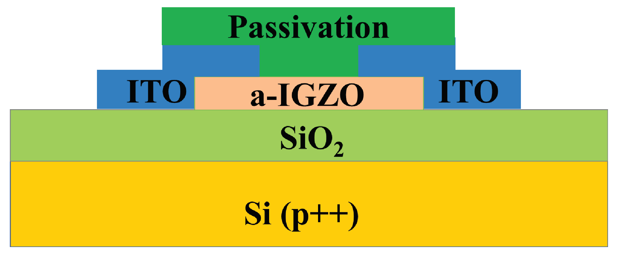
2. Materials and Methods

Inverted staggered a-IGZO TFTs were fabricated, the schematic cross-section of which is shown in Figure 1. P-type silicon wafers (gate electrodes) with a 200 nm-thick thermal SiO2 (gate insulators) were used as substrates. After thorough cleaning, 50 nm-thick a-IGZO films (In:Ga:Zn = 1:1:1 in mol ratio) as the channel layers were prepared on the substrates using radio frequency (RF) magnetron sputtering at room temperature (RT) with a power of 60 W, a pressure of 5 mTorr, and an Ar flow rate of 30 sccm. Then, Indium Tin Oxide (ITO) films with a thickness of 200 nm were deposited as source/drain (S/D) electrodes using direct current (DC) magnetron sputtering at RT, where the power was 100 W, the pressure was 5 mTorr, and the Ar flow rate was 30 sccm. For the passivated devices, SiO2 (or Al2O3) films with different thicknesses were deposited using RF sputtering at RT with ta power of 50 W, a pressure of 5 mTorr, and an Ar flow rate of 30 sccm. The channel layers, S/D electrodes, and PV layers were patterned using shadow masks during their depositions, leading to a channel width/length (W/L) of 1000/275 μm. Finally, the devices were annealed at 400 °C for 1 h.
The electrical characteristics of the TFTs were measured using a 2636 A parameter analyzer (Keithley Instruments, Inc., Beaverton, OR, USA) in an unsealed chamber, which maintained the atmospheric pressure and little gas circulation. The moisture content in the chamber was controlled by feeding the water molecules with the flow of N2. All the devices were measured at RT in darkness. For the transfer curve measurements, VDS of 10 V was employed. In this study, Vth is defined as the gate voltage of the normalized drain current (IDS/(W/L)) reaching 100 nA.

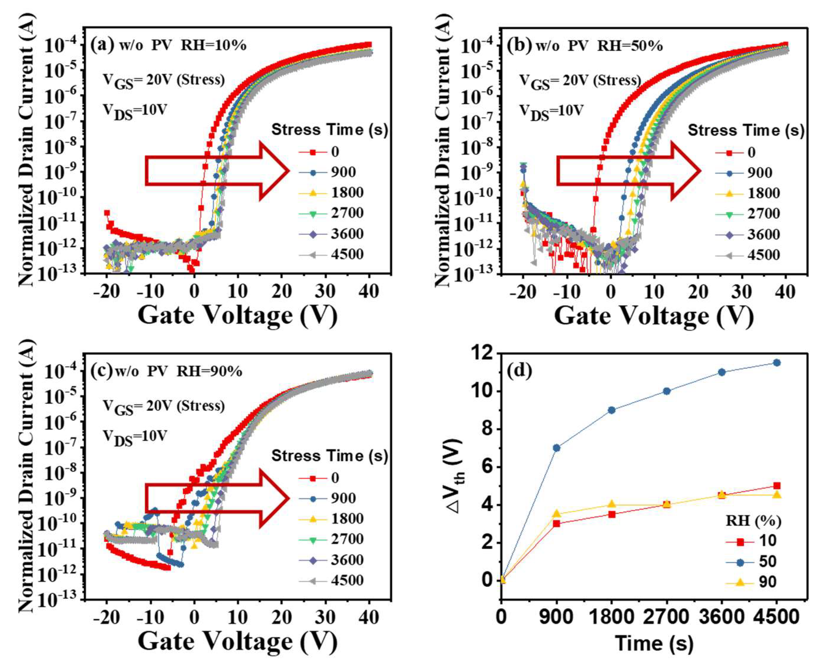
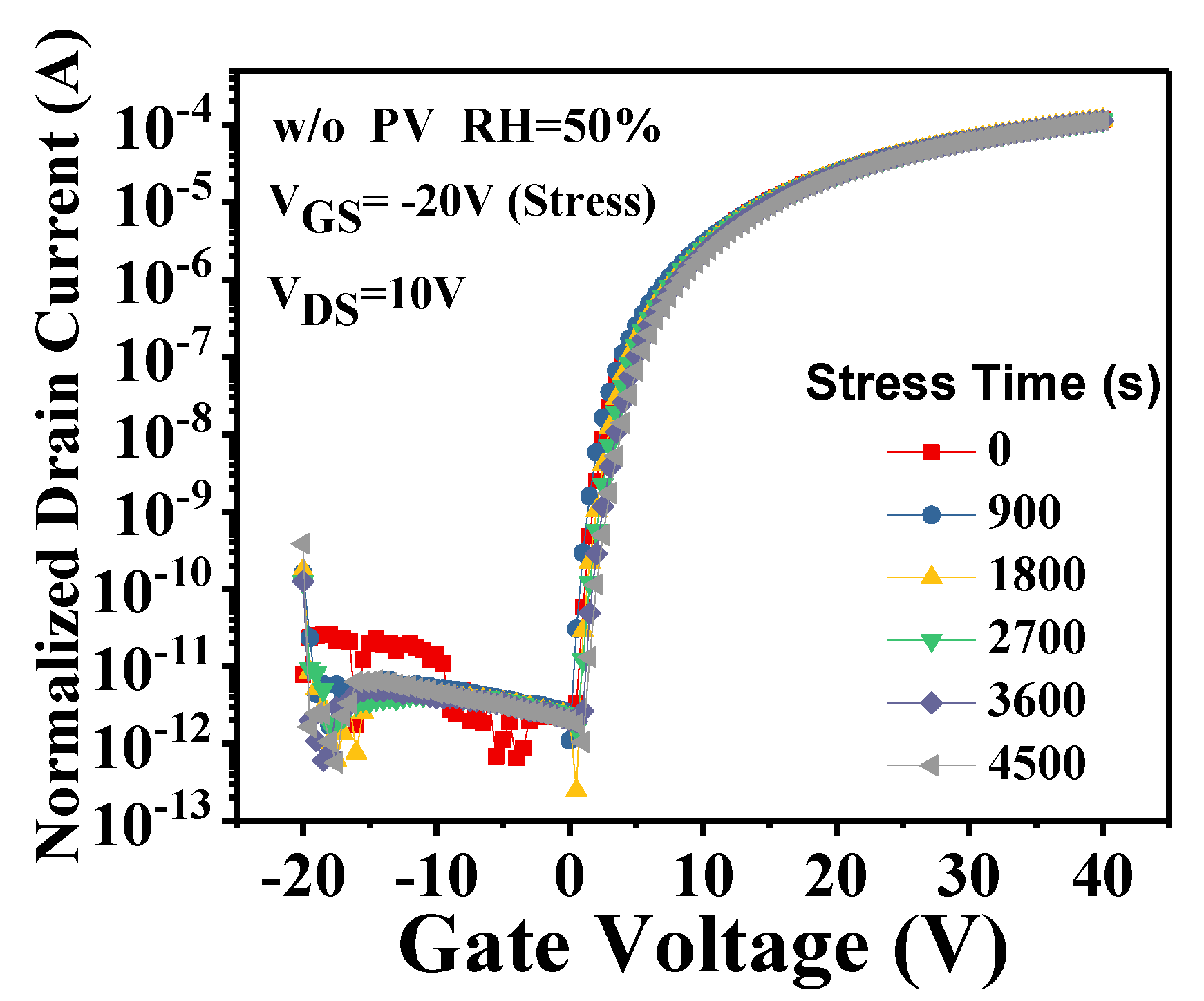
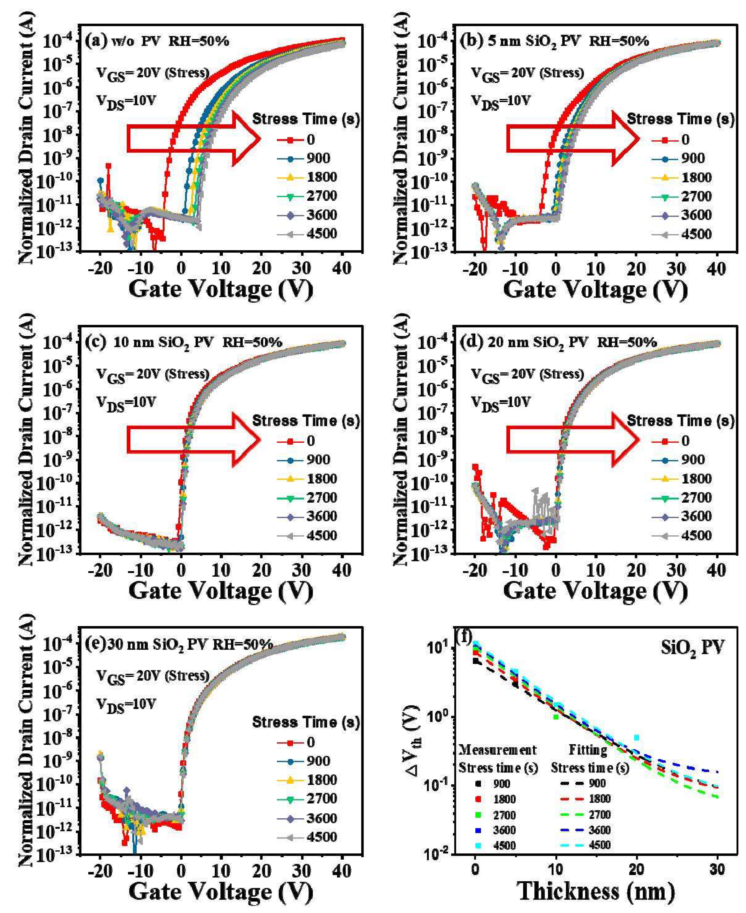
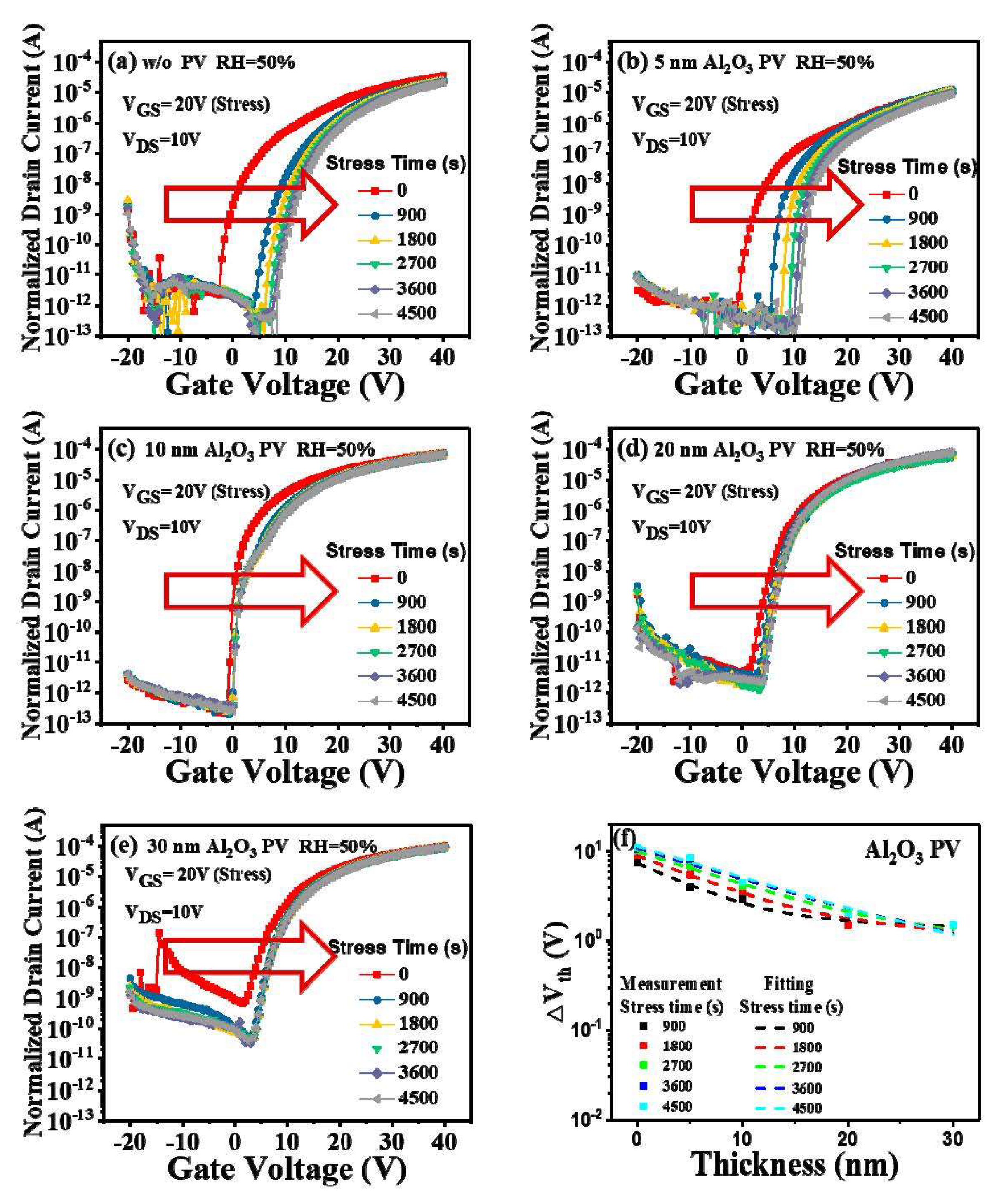
3. Results and Discussion

Figure 2a,c shows the time evolution of the transfer characteristics of the unpassivated a-IGZO TFTs under PGBS as well as the relative humidity (RH) of 10%, 50%, and 90%, respectively. During the PGBS tests, direct voltage of +20 V was applied to the gate electrodes for a period and then the transfer curves were instantly measured. With the increase in the stress time, the transfer curve positively shifted, which was apparently influenced by RH. In order to quantitatively describe the stable properties of a-IGZO TFTs under PGBS, we defined a useful term ΔVth, the difference between the Vth under stress and its initial value. The ΔVth values under various RH were extracted and listed in Figure 2d. After 4500 s of PGBS test, the positive Vth shifts of 5 V, 11.5 V, and 4.5 V were observed under RH = 10%, 50%, and 90%, respectively. It is worth noting that the largest ΔVth occurred at RH = 50% (as shown in Figure 2d), which is consistent with our previous report [22].
The positive Vth shift of a-IGZO TFTs under PGBS was attributed to charge trapping at the dielectric/channel interface (front-channel effect) [3,4,5,6], ambient atmosphere effects at the back surface (back-channel effect) [7,8,9,10,11,12,13,14], or bulk trapping in the IGZO bulk (bulk effect) [15,16]. According to our previous work [22], The biggest Vth shift at RH = 50% is mainly attributed to the competition of oxygen (or moisture) adsorption/desorption at the IGZO back surface during PGBS tests. This result indicates that RH = 50% is the severest condition to characterize the bias-stress stability of a-IGZO TFTs.
In addition, we measured the negative gate bias-stress (NGBS) instability of a-IGZO TFTs at RH = 50%, as shown in Figure 3. During the NGBS tests, a direct voltage of −20 V was applied to the gate electrodes for a period and then the transfer curves were instantly measured. After 4500 s of NGBS test, nearly no Vth shift was observed. When a negative voltage was applied to the gate electrode of a-IGZO TFTs, the oxygen atoms in a-IGZO tended to be repelled into the ambience, leading to negative shifts of Vth [25]. However, this process might have been effectively prohibited by the moisture-assisted oxygen adsorption [11,12,22], especially when the ambient RH was high. Therefore, no evident Vth shifts were exhibited during the NGBS tests in this study.
In this study, we deliberately adopted the severest measurement condition (RH = 50%) to examine the influence of PV layers on the bias-stress stability of a-IGZO TFTs. Since the devices were rather stable during the NGBS tests, only PGBS stabilities were characterized for the following studies.
It is well-known that PV layers can effectively improve the stability of TFT devices, whereas the exact physical mechanism involved is still not very clear. However, we may phenomenally describe the dependence of Vth shift (ΔVth) during PGBS tests on PV layer thickness (d) as follows [19],
Δ V th = α · e τ d + β
where β is the Vth shift affected by charge trapping, bulk trapping, and plasma damage, α is a constant relating to the Vth shift affected by ambient atmosphere, and ε is the characteristic length related to the gas diffusion. When d is larger than ε, the ambient gases hardly influence the PGBS stability of a-IGZO TFTs. In other words, the characteristic length ε is the critical dimension for the ambient atmosphere effect during PGBS tests. From an application perspective, a small ε is usually preferred.
To further investigate the ambient effects during PGBS tests, the a-IGZO TFTs were applied using PV layers with different thicknesses. SiO2, one of the most popular dielectric materials in TFT fabrications, was used to passivate the devices here. For comparison purposes, Al2O3, another dense material [23], was also adopted as PV layers for the a-IGZO TFTs in this study. The water vapor transmission rate (WVTR) and oxygen transmission rate (OTR) are reported to be inversely proportional to the PV layer thickness [24]. To analyze the influence of PV layers on PGBS stability of a-IGZO TFTs in depth, SiO2 and Al2O3 films with different thicknesses (0–30 nm) were deposited to passivate the devices.
Figure 4a,e shows the PGBS time evolution of the transfer characteristics of the a-IGZO TFTs with a SiO2 PV layer thickness of 0 nm, 5 nm, 10 nm, 20 nm, and 30 nm, respectively. We noticed that the passivated a-IGZO TFTs exhibited a similar tendency to that of the unpassivated device, i.e., with the increase in the stress time, the transfer curve gradually shifted in the positive direction. However, the a-IGZO TFTs with SiO2 PV showed more stable properties during the PGBS tests. To describe this tendency more clearly, we extracted the Vth shifts and listed them in Figure 4f. When the PV layer thickness increased from 0 nm to 30 nm, the ΔVth decreased evidently from 12 V to nearly 0.1 V after 4500 s of bias stress test. This can be attributed to the PV layer barrier effect, i.e., preventing the exchange of O2/H2O molecules between the channel layers and the ambient atmosphere. When the PV layer thickness was larger than 5 nm, the Vth of the a-IGZO TFTs barely changed. This can be understood by considering the concept of characteristic length (see (1)) in PV layers, which was about 5 nm here. When the SiO2 PV layer thickness was smaller than the characteristic length, the O2 molecules easily diffused from the atmosphere into a-IGZO (the H2O diffused inversely) under PGBS, resulting in positive Vth shifts of the a-IGZO TFTs. As the PV layer thickness was larger than ε, the diffusion of O2/H2O molecules through the PV layers became rather difficult. This is why the device with a thicker PV layer showed less degradation of its electrical behavior. Since a sufficiently thick PV could nearly eliminate the Vth shifts (as shown in Figure 4f), we can assume that the ambient atmosphere effect, rather than charge trapping, dominated the instability of a-IGZO TFTs during the PGBS tests in this study.
For comparison purposes, we also measured the PGBS stability of the a-IGZO TFTs passivated by Al2O3 PV layers with a thickness of 0 nm, 5 nm, 10 nm, 20 nm, and 30 nm, respectively, as shown in Figure 5a–e. We may observe that a fairly similar tendency to the case of SiO2-passivated devices was obtained here, i.e., the a-IGZO TFTs under PGBS became increasingly stable with the increase in the Al2O3 PV layer thickness. Meanwhile, for both Al2O3 and SiO2 PVs, the transfer curve positively shifted as the PV layer thickness increased, which can be attributed to the extra interface states generated during the PV depositions [26,27]. However, the Al2O3 PV layer also exhibited something different. As shown in Figure 5e, for the device with a thick PV layer (≥20 nm), its leakage current gradually rose with the increase in the stress time. This phenomenon was probably due to the plasma bombardment on the surface. Since the deposition rate of Al2O3 (0.7 nm/min) was smaller than that of SiO2 (1.5 nm/min), more sputtering time was needed for the deposition of the Al2O3 PV layers, leading to more serious plasma damage at the back channels. What is more, the ion bombardment of the plasma can result in a positive Vth shift [17,18], which explains why the leakage current of the devices with thick Al2O3 PV layers increased during the PGBS tests.
To precisely denote the influence of the Al2O3 PV layer on the PGBS stability of a-IGZO TFTs, the Vth shifts were extracted and listed in Figure 5f. Compared with the data shown in Figure 4f, we may note that the Al2O3 PV layers had an inferior barrier function to SiO2. When the Al2O3 PV layer thickness was larger than 10 nm, the Vth shift of the devices changed slightly, indicating that the characteristic length of the Al2O3 PV layer was around 10 nm. When the PV layer thickness reached 30 nm, the ΔVth became much smaller (~1 V), again confirming that the ambient atmosphere effect dominated during the PGBS tests in this study.
So far, we have obtained two important experimental results: (1) the PGBS stability of a-IGZO TFTs gradually improved with the increase in PV layer thickness; (2) the SiO2 PV layer exhibited a better improvement effect on the PGBS stability than Al2O3. In order to discuss the theoretical origin of these results, we extracted the critical parameters in (1) of the PV layers. We fit the measurement data of SiO2 PV and Al2O3 PV with (1), as shown in Figure 4f and Figure 5f, respectively. One may observe that the fitting curves agreed well with the measurement data, from which the fitting parameters were obtained and summarized in Table 1.
As shown in Table 1, the α values of both PV layers were much larger than the β values for the same stress time, indicating that the ambient atmosphere effect instead of charge trapping dominated during the PGBS tests in this study. Therefore, with the increase in PV layer thickness, the ambient atmosphere effect was more strongly prevented, resulting in better PGBS stability of a-IGZO TFTs. The α value increased with the increase in the bias time, whereas the ε remained nearly unchanged. The increase in α resulted from more O2/H2O exchange between the device back channels and the ambience, leading to a larger Vth shift. Most importantly, SiO2 and Al2O3 exhibited quite different characteristic length (ε) values, as shown in Table 1. The characteristic length of the SiO2 PV layers (~5 nm) was far smaller than that of Al2O3 (~10 nm), leading to better improvement of the PGBS stability of a-IGZO TFTs by SiO2 PV layers than Al2O3. Therefore, based on our results, the sputtered SiO2, rather than the sputtered Al2O3, should be preferred to passivate a-IGZO TFTs in applications of FPDs.

4. Conclusions

The transfer curve of a-IGZO TFTs shifted positively during the PGBS tests, which could effectively be improved by applying PV layers. In this work, both SiO2 and Al2O3 films with different thicknesses were used to passivate the a-IGZO TFTs, indicating that the ambient atmosphere effect rather than charge trapping dominated the Vth shifts during the PGBS tests. A simple model was used to theoretically discuss the related physical mechanism. With the increase in PV layer thickness, the devices became increasingly stable, as a result of the stronger prevention of the ambient atmosphere effect. When the PV layer thickness reached the characteristic length, the variation in Vth became quite small. The SiO2 PV layer showed a better improvement effect than the Al2O3 PV layer because the former had a smaller characteristic length.

Author Contributions

Y.Z. fabricated and measured all the a-IGZO TFTs. Y.Z. and C.D. designed the experiments and contributed to the theoretical explanations. The manuscript was written by Y.Z. and C.D.

Funding

This work was supported by the Natural Science Foundation of China (grant No. 61474075).

Conflicts of Interest

The authors declare no conflict of interest.

References

  1. Nomura, K.; Ohta, H.; Takagi, A.; Kamiya, T.; Hirano, M.; Hosono, H. Room-temperature fabrication of transparent flexible thin-film transistors using amorphous oxide semiconductors. Nature 2004, 432, 488–492. [Google Scholar] [CrossRef] [PubMed]
  2. Kim, M.K.; Jeong, J.H.; Lee, H.J.; Ahn, T.K.; Shin, H.S.; Park, J.S.; Jeong, J.K.; Mo, Y.G.; Kim, H.D. High mobility bottom gate InGaZnO thin film transistors with SiOx etch stopper. Appl. Phys. Lett. 2007, 90, 212114. [Google Scholar] [CrossRef]
  3. Suresh, A.; Muth, J.F. Bias stress stability of indium gallium zinc oxide channel based transparent thin film transistors. Appl. Phys. Lett. 2008, 92, 033502. [Google Scholar] [CrossRef]
  4. Lee, J.M.; Cho, I.T.; Lee, J.H.; Kwon, H.I. Bias-stress-induced stretched-exponential time dependence of threshold voltage shift in InGaZnO thin film transistors. Appl. Phys. Lett. 2008, 93, 093504. [Google Scholar] [CrossRef]
  5. Chen, T.C.; Chang, T.C.; Hsieh, T.Y.; Lu, W.S.; Jian, F.Y.; Tsai, C.T.; Huang, S.Y.; Lin, C.S. Investigating the degradation behavior caused by charge trapping effect under DC and AC gate-bias stress for InGaZnO thin film transistor. Appl. Phys. Lett. 2011, 99, 022104. [Google Scholar] [CrossRef]
  6. Kim, S.J.; Lee, S.Y.; Lee, Y.W.; Kuk, S.H.; Kwon, J.Y.; Han, M.K. Effect of Charge Trapping/Detrapping on Threshold Voltage Shift of IGZO TFTs under AC Bias Stress. Electrochem. Solid-State Lett. 2012, 15, H108–H110. [Google Scholar] [CrossRef]
  7. Sung, S.Y.; Choi, J.H.; Han, U.B.; Lee, K.C.; Lee, J.H.; Kim, J.J.; Lim, W.; Pearton, S.J.; Norton, D.P.; Heo, Y.W. Effects of ambient atmosphere on the transfer characteristics and gate-bias stress stability of amorphous indium-gallium-zinc oxide thin-film transistors. Appl. Phys. Lett. 2010, 96, 102107. [Google Scholar] [CrossRef]
  8. Jeong, J.K.; Yang, H.W.; Jeong, J.H.; Mo, Y.G.; Kim, H.D. Origin of threshold voltage instability in indium-gallium-zinc oxide thin film transistors. Appl. Phys. Lett. 2008, 93, 123508. [Google Scholar] [CrossRef]
  9. Liu, P.T.; Chou, Y.T.; Teng, L.F. Environment-dependent metastability of passivation-free indium zinc oxide thin film transistor after gate bias stress. Appl. Phys. Lett. 2009, 95, 233504. [Google Scholar] [CrossRef]
  10. Chen, Y.C.; Chang, T.C.; Li, H.W.; Chen, S.C.; Lu, J.; Chung, W.F.; Tai, Y.H.; Tseng, T.Y. Bias-induced oxygen adsorption in zinc tin oxide thin film transistors under dynamic stress. Appl. Phys. Lett. 2010, 96, 262104. [Google Scholar] [CrossRef]
  11. Zhang, J.; Li, X.F.; Lu, J.G.; Zhou, N.J.; Guo, P.J.; Lu, B.; Pan, X.H.; Chen, L.X.; Ye, Z.Z. Water assisted oxygen absorption on the instability of amorphous InAlZnO thin-film transistors. RSC Adv. 2014, 4, 3145–3148. [Google Scholar] [CrossRef]
  12. Chung, W.F.; Chang, T.C.; Li, H.W.; Chen, S.C.; Chen, Y.C.; Tseng, T.Y.; Tai, Y.H. H2O-Assisted O2 Adsorption in Sol-Gel Derived Amorphous Indium Gallium Zinc Oxide Thin Film Transistors. Electrochem. Solid State Lett. 2011, 14, H235–H237. [Google Scholar] [CrossRef]
  13. Huang, S.Y.; Chang, T.C.; Chen, M.C.; Chen, S.C.; Tsai, C.T.; Hung, M.C.; Tu, C.H.; Chen, C.H.; Chang, J.J.; Liau, W.L. Effects of Ambient Atmosphere on Electrical Characteristics of Al2O3 Passivated InGaZnO Thin Film Transistors during Positive-Bias-Temperature-Stress Operation. Electrochem. Solid State Lett. 2011, 14, H177–H179. [Google Scholar] [CrossRef]
  14. Chen, F.H.; Pan, T.M.; Chen, C.H.; Liu, J.H.; Lin, W.H.; Chen, P.H. Two-step Electrical Degradation Behavior in α-InGaZnO Thin-film Transistor Under Gate-bias Stress. IEEE Electron Device Lett. 2013, 34, 635–637. [Google Scholar] [CrossRef]
  15. Cho, E.N.; Kang, J.H.; Yun, I. Effects of channel thickness variation on bias stress instability of InGaZnO thin-film transistors. Microelectron. Reliab. 2011, 51, 1792–1795. [Google Scholar] [CrossRef]
  16. Li, J.; Ding, X.W.; Zhang, J.H.; Zhang, H.; Jiang, X.Y.; Zhang, Z.L. Improving electrical performance and bias stability of HfInZnO-TFT with optimizing the channel thickness. AIP Adv. 2013, 3, 102132. [Google Scholar] [CrossRef] [Green Version]
  17. Lin, W.K.; Liu, K.C.; Chen, J.N.; Hu, S.C.; Chang, S.T. The influence of fabrication process on top-gate thin-film transistors. Thin Solid Films 2011, 519, 5126–5130. [Google Scholar] [CrossRef]
  18. Lin, W.K.; Liu, K.C.; Chang, S.T.; Li, C.S. Room temperature fabricated transparent amorphous indium zinc oxide based thin film transistor using high-κ HfO2 as gate insulator. Thin Solid Films 2011, 520, 3079–3083. [Google Scholar] [CrossRef]
  19. Li, G.T.; Yang, B.R.; Liu, C.; Lee, C.Y.; Tseng, C.Y.; Lo, C.C.; Lien, A.; Deng, S.Z.; Shieh, H.P.D.; Xu, N.S. Positive gate bias instability alleviated by self-passivation effect in amorphous InGaZnO thin-film transistors. J. Phys. D Appl. Phys. 2015, 48, 475107. [Google Scholar] [CrossRef]
  20. Fan, C.L.; Shang, M.C.; Li, B.J.; Lin, Y.Z.; Wang, S.J.; Lee, W.D.; Hung, B.R. Teflon/SiO2 bilayer passivation for improving the electrical reliability of oxide TFTs fabricated using a new two-photomask self-alignment process. Materials 2015, 8, 1704–1713. [Google Scholar] [CrossRef] [PubMed]
  21. Li, J.; Zhou, F.; Lin, H.P.; Zhu, W.Q.; Zhang, J.H.; Jiang, X.Y.; Zhang, Z.L. Effect of reactive sputtered SiOx passivation layer on the stability of InGaZnO thin film transistors. Vacuum 2012, 86, 1840–1843. [Google Scholar] [CrossRef]
  22. Zhou, Y.; Xu, J.; Xie, H.; Zhang, L.; Liu, G.; Tong, X.; Dong, C. Moisture Dominant Electrical Degradation of Amorphous InGaZnO Thin Film Transistors under Positive Bias Stress. In Proceedings of the International Display Workshop (IDW)’17, Sendai, Japan, 6–8 December 2017; pp. 424–426. [Google Scholar]
  23. Wu, J.; Chen, Y.; Zhou, D.; Hu, Z.; Xie, H.; Dong, C. Sputtered oxides used for passivation layers of amorphous InGaZnO thin film transistors. Mater. Sci. Semicond. Process. 2014, 29, 277–282. [Google Scholar] [CrossRef]
  24. Graff, G.L.; Burrows, P.E.; Williford, R.E.; Praino, R.F. Barrier Layer Technology for Flexible Displays. In Flexible Flat Panel Display, 1st ed.; Crawford, G.P., Ed.; Brown University: Providence, RI, USA, 2005; pp. 57–60. ISBN 0-470-87048-6. [Google Scholar]
  25. Chen, Y.C.; Chang, T.C.; Li, H.W.; Chen, S.C.; Chung, W.F.; Chen, Y.H.; Tai, Y.H.; Tseng, T.Y.; Yeh, F.S. Surface states related the bias stability of amorphous In–Ga–Zn–O thin film transistors under different ambient gasses. Thin Solid Films 2011, 520, 1432–1436. [Google Scholar] [CrossRef]
  26. Chen, T.C.; Chang, T.C.; Hsieh, T.Y.; Tsai, C.T.; Chen, S.C.; Lin, C.S.; Hung, M.C.; Tu, C.H.; Chang, J.J.; Chen, P.L. Light-induced instability of an InGaZnO thin film transistor with and without SiOx passivation layer formed by plasma-enhanced-chemical-vapor-deposition. Appl. Phys. Lett. 2010, 97, 192103. [Google Scholar] [CrossRef]
  27. Ohara, H.; Sasaki, T.; Noda, K.; Ito, S.; Sasaki, M.; Endo, Y.; Yoshitomi, S.; Sakata, J.; Serikawa, T.; Yamazaki, S. 4.0-inch active-matrix organic light-emitting diode display integrated with driver circuits using amorphous In–Ga–Zn-Oxide thin-film transistors with suppressed variation. Jpn. J. Appl. Phys. 2010, 49, 03CD02. [Google Scholar] [CrossRef]
Figure 1. Schematic cross-section of the inverted staggered amorphous InGaZnO (a-IGZO) thin-film transistors (TFTs).
Micromachines 09 00603 g001
Figure 2. Transfer characteristics of the unpassivated a-IGZO TFTs as a function of the positive gate bias-stress (PGBS) time under relative humidity (RH) of (a) 10%, (b) 50%, and (c) 90%, respectively; (d) variations of the ΔVth with PGBS time for the a-IGZO TFT devices.
Micromachines 09 00603 g002
Figure 3. Transfer characteristics of the unpassivated a-IGZO TFTs as a function of the negative gate bias-stress (NGBS) time under RH = 50%.
Micromachines 09 00603 g003
Figure 4. Stress-time dependence of the transfer characteristics of the a-IGZO TFTs with a SiO2 PV layer thickness of (a) 0 nm, (b) 5 nm, (c) 10 nm, (d) 20 nm, and (e) 30 nm, respectively; (f) experimental data and fitting curves of the ΔVth under PGBS as a function of PV layer thickness of the a-IGZO TFTs.
Micromachines 09 00603 g004
Figure 5. Stress-time dependence of the transfer characteristics of the a-IGZO TFTs with an Al2O3 PV layer thickness of (a) 0 nm, (b) 5 nm, (c) 10 nm, (d) 20 nm, and (e) 30 nm, respectively; (f) experimental data and fitting curves of the ΔVth under PGBS as a function of the PV layer thickness of the a-IGZO TFTs.
Micromachines 09 00603 g005
Table 1. Fitting parameters of the PV layers used for a-IGZO TFTs.
MaterialsStress Time (s)α (V)β (V)ε (nm)
SiO29006.470.065.93
18008.460.075.22
2700100.045.03
360010.860.144.86
450011.450.065.13
Al2O39006.071.399.24
18007.951.099.53
27009.310.8410.21
360010.460.3011.23
450011.070.2511.06

