Article

Single and Repetitive Surge Reliability of 1200 V Asymmetric Trench SiC MOSFETs Under Various Gate Biases

1
State Key Laboratory of Wide-Bandgap Semiconductor Devices and Integrated Technology, Xidian University, Xi’an 710071, China
2
State Key Laboratory of Reliability Technology for Electronic Components, China Electronic Product Reliability and Environmental Testing Research Institute, Guangzhou 511370, China
3
Guangzhou Wide Bandgap Semiconductor Innovation Center, Guangzhou Institute of Technology, Xidian University, Guangzhou 510555, China
4
The School of Electronic Science and Engineering (School of Microelectronics), South China Normal University, Foshan 528225, China
5
The School of Materials Science and Engineering, South China University of Technology, Guangzhou 510641, China
*
Authors to whom correspondence should be addressed.
Micromachines 2026, 17(7), 823; https://doi.org/10.3390/mi17070823
Submission received: 10 June 2026 / Revised: 8 July 2026 / Accepted: 8 July 2026 / Published: 10 July 2026
(This article belongs to the Special Issue Emerging Technologies and Applications for Semiconductor Industry)

Abstract

The parameter degradation and failure mechanisms of 1200 V asymmetric trench-type (AT) silicon carbide (SiC) metal oxide semiconductor field-effect transistors (MOSFETs) under various single and repetitive surge currents, with various gate bias voltages (VGS) of 0 V, −5 V, and −10 V, are systematically investigated in this work. It is indicated that VGS has no impact on the single surge reliability, with the same maximum single surge current (SSCmax) under different VGS. However, during repetitive surge stress (90% and 60% SSCmax), the maximum surge cycles have increased as VGS increases from −10 V to 0 V. It may be caused by the enhancement of channel-assisted leakage conduction, allowing more surge current to flow through the channel. It is concluded from gate capacitance (Cg-Vg) and low-frequency noise (LFN) characterizations that lower VGS increases SiC/SiO2 interface defect density, accelerating parameter degradation during single and repetitive surge stress. Both chip and package failures are observed for single and repetitive surge stress. For single surge stress, the device failure has resulted from the melted source Al as the metal erodes and penetrates through the interlayer dielectric and the ohmic contact layer between the source metal and the SiC-doped region, respectively, leading to a three-terminal short circuit. For repetitive surge stress, the device failure has been caused by the penetration of Al metal into the interlayer dielectric, leading to a gate-source short circuit. This comprehensive research provides valuable guidance for enhancing the surge reliability of SiC MOSFETs.

1. Introduction

Power devices play a pivotal role in power electronics technology, performing critical functions such as electric energy conversion, power control, and system protection. With the rapid development of new energy technologies such as electric vehicles and other related fields, the performance and reliability of power devices directly influence the advancement and application scope of power electronics technology. In recent years, silicon carbide (SiC) metal oxide semiconductor field-effect transistors (MOSFETs) are increasingly replacing traditional silicon-based devices due to their advantages of high-frequency operation, high voltage capability, superior thermal stability, fast switching, and low power losses, and they have become the preferred choice for high power applications such as new energy vehicles, photovoltaic inverters, and industrial drives [1,2].
Commercially available SiC MOSFETs are currently categorized into three dominant architectures: planar-gate structure, symmetric double-trench structure, and asymmetric-trench (AT) structure [3]. Compared with planar and symmetric trench structures, AT SiC MOSFETs have attracted more and more attention with their advantages of simultaneous optimization of conduction performance and gate oxide reliability. The device utilizes the (11 2 ¯ 0) crystal plane for its conductive channel, which exhibits an extremely low interface state density and oxide trap concentration at the SiC/SiO2 interface. This significantly enhances channel electron mobility, thereby substantially reducing the device’s specific on-state resistance (RDS(on)). Concurrently, a deep p+ shielding region has been introduced on one side, and it effectively suppresses electric field crowding at the trench corners, preventing premature breakdown of the gate oxide layer [4].
As power density and switching frequency continue to increase, surge reliability has become a critical reliability concern, limiting the large-scale application of SiC MOSFETs [5]. Under actual operating conditions such as motor startup, lightning strikes, and so on, the devices endure surge stresses that far exceed their rated current [6]. Although the deep p+ well optimizes the electric-field distribution for AT SiC MOSFETs, a distorted current distribution readily occurs during freewheeling of the intrinsic body diode, which directly induces gate oxide degradation and a thermal concentration effect, drastically deteriorating the device’s surge ruggedness [7].
Currently, the surge reliability of SiC MOSFETs are the focus of research [8,9,10,11,12,13,14,15,16,17,18]. However, relevant studies have mainly focused on conventional planar-gate structures and symmetrical double-trench structures [8,9,10,11,12,13,14,15,16,17], with relatively limited investigations into asymmetric trench structures. Meanwhile, most existing literature has only studied either single or repetitive surge reliability for SiC MOSFETs [9,10,11,12,13,14,15,16,17,18], and there is still a lack of systematic investigation on the parameter degradation and failure mechanism under both single and repetitive stresses. Furthermore, although the impact of gate-source voltage (VGS) amplitude on single-surge reliability has been studied in the literature [11,12,13,14,15,16,17,18], research on the effect of VGS on the repetitive surge reliability of SiC MOSFETs is relatively scarce, especially for AT SiC MOSFETs. In addition, the effect of varying repetitive surge current amplitudes on SiC MOSFET reliability has rarely been studied.
Thus, the parameter degradation and failure mechanisms of 1200 V AT SiC MOSFETs under single and repetitive surge stress with varying VGS and surge current amplitudes are systematically investigated in this work. Three samples are tested for each condition during the surge experiments to ensure the reliability of the results. During the surge test, the degradation behaviors of key parameters, including three-terminal resistance, threshold voltage (VTH), on-state resistance, body diode voltage drop (VSD), drain-source leakage current (IDSS), gate-source leakage current (IGSS), subthreshold swing (S.S.), gate capacitance (Cg-Vg), and low-frequency noise (LFN) characteristics, are summarized. Meanwhile, failure modes and mechanisms of the devices are clarified through multiple characterization techniques, such as X-ray inspection, scanning acoustic microscopy (SAM), and post decapsulation scanning electron microscopy (SEM).

2. Experiment Introduction

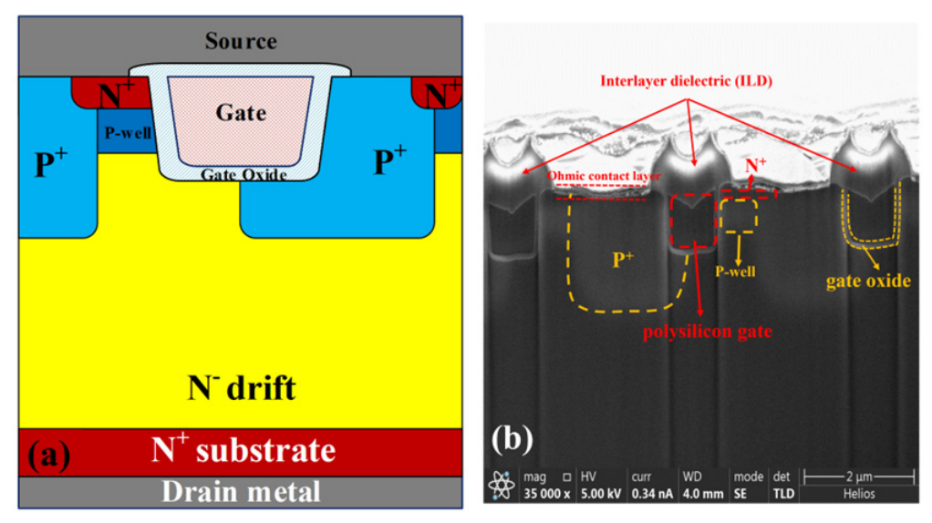
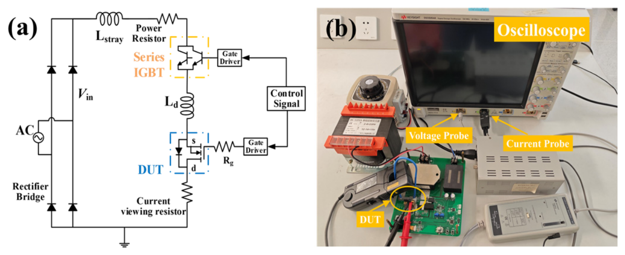
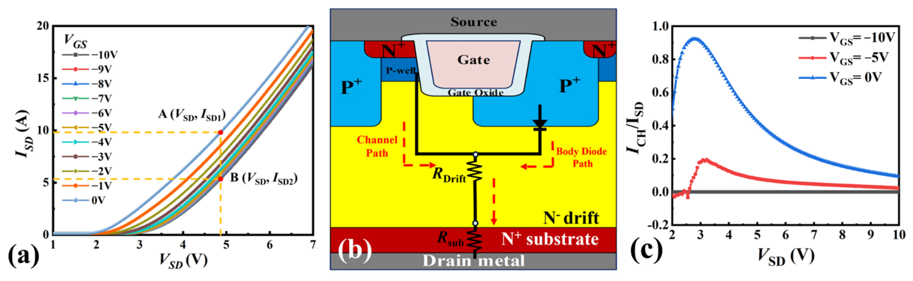
The devices under test (DUTs) are commercially available 1200 V AT SiC MOSFETs with a rated current of 36 A. Figure 1 illustrates the device structure and cross-sectional view. During the surge pulse test, half-wave sinusoidal currents of a 10 ms duration are injected through the DUTs. The simplified test circuit and surge test platform are shown in Figure 2a,b, and this circuit is employed to assess the single and repetitive surge pulse current withstanding capabilities and parameter degradation behavior of the SiC MOSFETs. Figure 3a presents the third-quadrant I–V characteristic curves. When VGS is less than or equal to −9 V, the curves remain essentially unchanged, indicating that the current conduction is dominated by the body diode with a negligible contribution of the channel-assisted leakage conduction, resulting in an identical ISD at the same VSD. As VGS increases from −9 V to 0 V, the ISD increases under the same VSD. At this stage, the MOS channel is partially turned on, providing an additional current path. The surge current path is shown in Figure 3b, where the current flows from the source to the N drift region through both the body diode and the MOS channel in parallel before reaching the drain [18,19]. Equation (1) defines the proportion of channel current (ICH) to the source-drain current ISD [20]:
I C H I S D 1 = I S D 1 I S D 2 I S D 1 .
Point A (VSD, ISD1) is selected on the curve at VGS = 0 V and point B (VSD, ISD2) is selected at VGS = −10 V, sharing the same voltage coordinate (VSD) as point A. The difference between the two points arises from the current at point A (ISD1), which includes both the current flowing through the channel (ICH) and the body diode, whereas the current at point B (ISD2) only contains the current flowing through the body diode. As is visually evident from Figure 3c, with the increase in VSD, the proportion of ICH at VGS = 0 V and VGS = −5 V shows a downward trend. In the main range of VSD, the body-diode current dominates for a larger fraction, indicating that the surge current continues to be dominated by body diode conduction.
Based on these observations, surge current tests are conducted under three VGS: VGS = 0 V, –5 V, and –10 V, corresponding to different channel states, respectively (Table 1). VTH is measured in accordance with the JEDEC standard JEP 183A using the constant current method [21]. To suppress the hysteresis effect in the extracted VTH, a positive gate preconditioning pulse VGS(MAX) is applied before the down-sweep phase, and VTH is extracted during the down-sweep at VGS = VDS and IDS = 5 mA.

3. Results and Discussion

3.1. Single-Pulse Surge Test

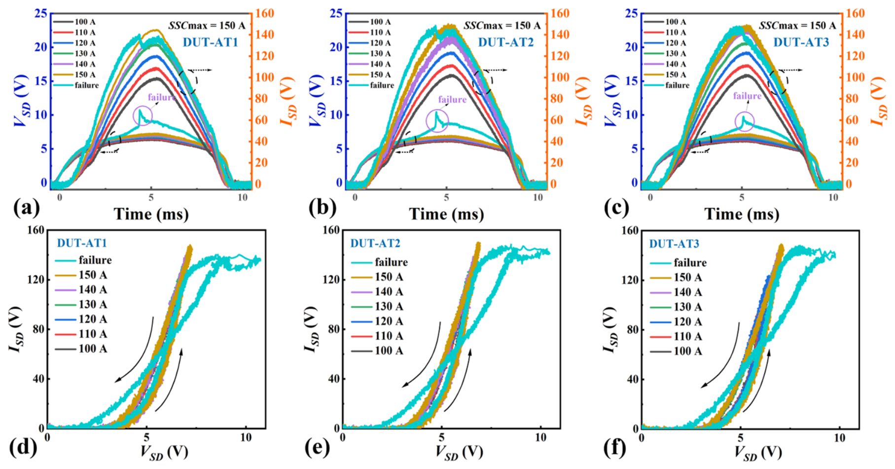
Firstly, a single-pulse surge test is conducted on the AT SiC MOSFETs under various VGS. The surge current starts at 100 A and is increased in steps of 10 A until device failure occurs. A 10-min interval is maintained between the successive pulses to ensure adequate cooling and prevent thermal accumulation. The surge current waveforms and corresponding current trajectories are shown in Figure 4, where the VGS for DUT-AT1, DUT-AT2, and DUT-AT3 is set at 0 V, −5 V, and −10 V, respectively. A voltage spike is observed in VSD at the moments of device failure. Under the maximum single surge current stress (SSCmax), the waveforms of VSD and ISD remain consistent. The SSCmax for all devices is uniformly 150 A. The surge trajectories of the DUTs exhibit a counterclockwise direction, indicating that the body diode conduction mechanism is dominant under these conditions [22].
Subsequently, a first-order estimation of the junction temperature under surge stress is conducted using the transient thermal impedance method (Foster thermal equivalent circuit) [23]. The instantaneous power dissipation is calculated from the measured voltage and current waveforms as P(t) = V(t)I(t). The single-pulse dissipated energy is calculated as follows:
E p l u s e = 0 t p V S D t I S D t   d t .
The junction temperature rise is then estimated by convolving the power waveform with the transient thermal impedance (Zthjc(t)) obtained from the device datasheet. The device junction temperature is calculated as follows:
T j t = T c + T j c t = T c + P t Z t h j c ( t ) ,
where Tc = 303 K is defined as the case temperature. Although this method does not provide spatial temperature distribution as finite-element thermal simulation does, it provides a conservative first-order correlation between the surge current stress and junction temperature rise. The relevant parameters for various VGS biases are listed in Table 2. Although VGS slightly changes the voltage drop and pulse energy, the measured SSCmax remains unchanged within the experimental current-step resolution. This indicates that the single surge failure threshold is not sufficiently sensitive to the small VGS-induced difference in single-pulse energy. Conversely, repetitive degradation is significantly affected by the VGS-induced difference, as detailed in Section 3.2 and Section 3.3.
In this work, the DUTs’ surge capability is defined as:
S u r g e   c a p a b i l i t y = I F S M I r a t e d ,
where IFSM is the DUTs’ surge current at the moments of failure and Irated represents the rated current of the DUTs at 298 K, which is 36 A [19]. After each surge pulse, the resistances between the three terminals of the devices (RGS, RSG, RDS, RSD, RGD, and RDG) are measured for preliminary evaluation. The values are recorded when the devices fail, and these are summarized in Table 3. The relatively low resistances observed across all three terminals under the different VGS indicate that short circuit occurs among the terminals of the DUTs, along with internal structural damage.
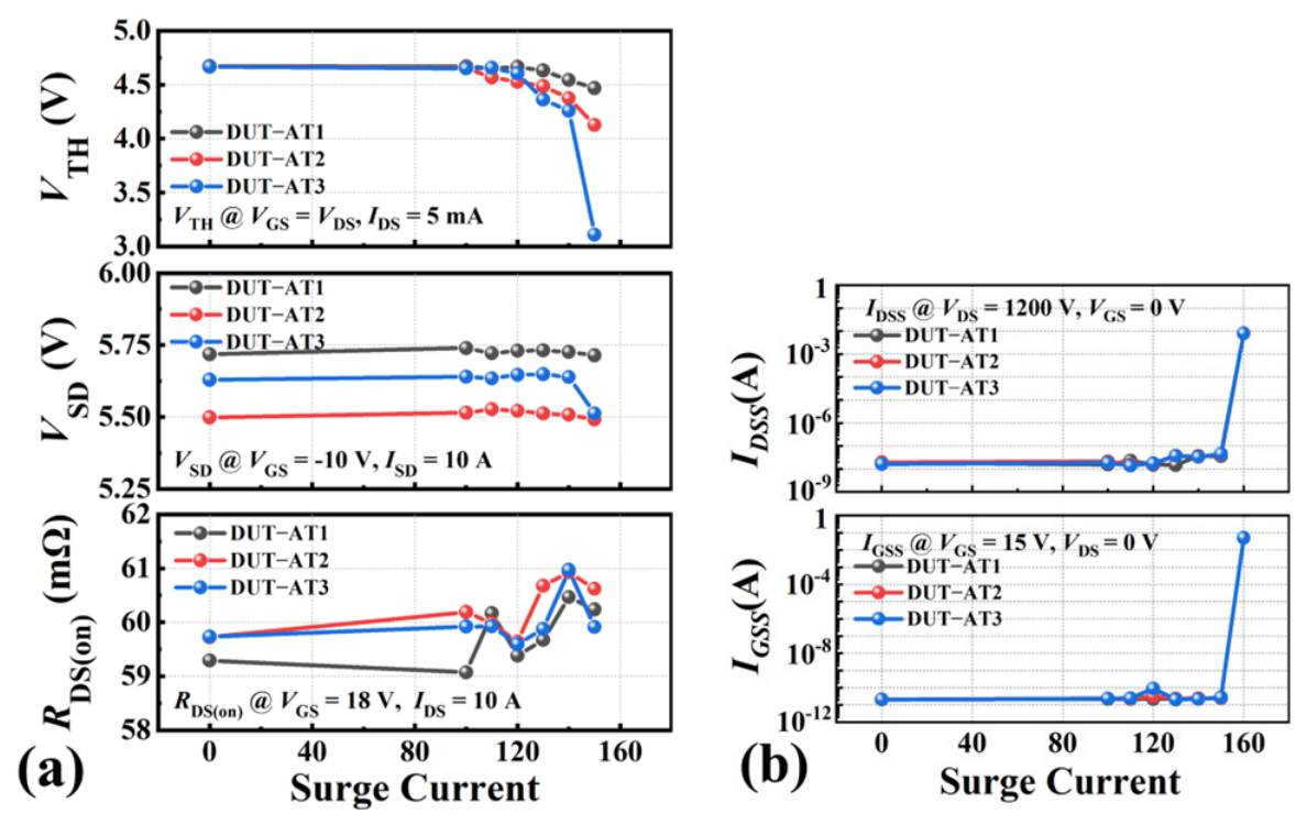
Figure 5 illustrates the degradation of the electrical parameters after each surge pulse. VTH, VSD, and RDS(on) become unmeasurable when device failure occurs. VGS significantly influences parameter degradation prior to total failure. DUT-AT1, AT2, and AT3 exhibit negative VTH shifts under varying VGS. DUT-AT3 shows the most severe degradation, with a 33.34% reduction in VTH, while DUT-AT1 and AT2 show decreases of 4.36% and 11.61%, respectively. The more pronounced VTH negative shift at a more negative VGS is attributed to the stronger electric field at the gate–oxide interface of the DUTs (from the substrate to the gate electrode), which elevates the impact ionization rate along the sloped trench sidewalls and ultimately facilitates the injection of holes into the gate oxide layer [24]. Simultaneously, RDS(on) shows a slight upward trend following the increasing surge current. The ∆VSD remains below 1% for DUT-AT1 and AT2, yet AT3 exhibits the largest VSD change, with a reduction of approximately 2.1%. Drain-source leakage current (IDSS) and gate leakage current (IGSS) remain nearly identical under different VGS until device failure, where both currents sharply increase to the milliampere (mA) level, indicating the loss of gate control over the channel and voltage blocking capability between the drain and source.
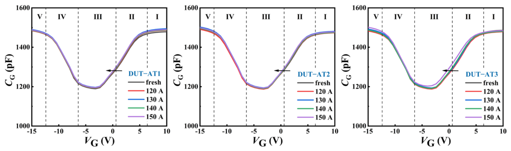
The changes in the Cg-Vg characteristics of the DUTs are presented in Figure 6. The waveform changes primarily occur in Region II and Region III, indicating that the degradation is concentrated at the edge of the gate oxide layer or the trench sidewall of the devices [25,26]. As gate-bias voltage stress decreases from 0 V to −10 V, the Cg-Vg curves shift further to the left, consistent with the VTH degradation trend. It is indicated that the increased density of the interface traps caused by more negative VGS intensifies gate-oxide deterioration and correspondingly lowers VTH under single-pulse surge current stress, consistent with the literature [27].
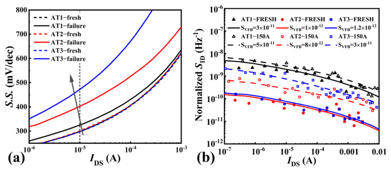
Figure 7a shows the variation in S.S. under different VGS. S.S. increases significantly after surge stress, indicating degradation of the gate oxide layer. Under the effect of surge stress, additional electron traps are generated at the SiC/SiO2 interface, with higher trap density observed at lower VGS. Figure 7b illustrates the relationship between the normalized noise power spectral density measured at 10 Hz and IDS before and after the single surge current stress. The low-frequency noise power spectral density of DUT-AT1, AT2, and AT3 increase by 0.67, 7, and 10.83 times, respectively, after single surge stress compared to their initial values, which is consistent with Cg-Vg and VTH variations. This may be attributed to the higher localized electric field stress caused by the more negative VGS, which amplifies the generation of interface traps and oxide traps under surge stress. These traps facilitate the carrier trapping and release processes [28,29].

3.2. Repetitive Surge Test at 90% SSCmax

For the repetitive surge test, the time interval between each surge pulse is set to 10 s to avoid heat accumulation within the devices. The values of 90% and 60% of SSCmax are selected for the repetitive surge current stress. Here, 90% SSCmax serves as the extreme condition for assessing thermomechanical failure margins, while 60% SSCmax acts as the moderate condition for reflecting gradual degradation. These stress levels effectively accelerate the degradation process while avoiding sudden the catastrophic failures caused by a single-pulse surge, consistent with existing studies where surge amplitudes typically fall within 60–90% of SSCmax [8,9,10,30].
VGS for DUT-AT4, AT5, and AT6 are set at 0 V, −5 V, and −10 V, respectively, with a repetitive surge current amplitude of 135 A, corresponding to 90% of the maximum single surge current. The maximum surge cycles to failure and the three-terminal resistances at the point of failure are summarized in Table 4. It is indicated that the number of surge current cycles the device can withstand decreases as VGS becomes more negative. This may be caused by a weaker contribution of channel-assisted leakage conduction, which leads to more current flowing through the body diode during repetitive surge current stress. Meanwhile, DUT-AT4, AT5, and AT6 exhibit a significant reduction in gate-source resistance when the devices fail, indicating that gate-source short circuit occurs.
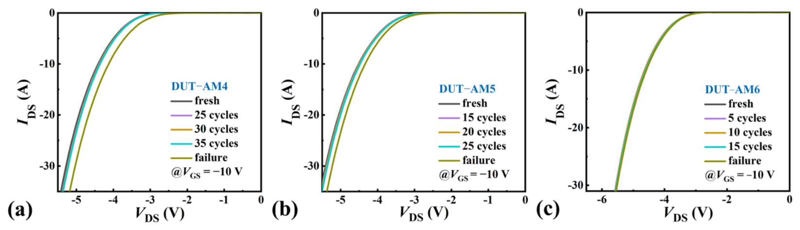
Figure 8 shows the changes in the third-quadrant characteristics of DUT-AT4, AT5, and AT6 under repetitive surge stress. When the devices fail, the knee voltage and forward drop of the body diode in DUT-AT4 decrease from 2.9 V and 4.3 V to 2.3 V and 4.1 V, respectively, indicating a gate-source short circuit and reduction in the body diode conduction barrier. However, for DUT-AT5, the knee voltage and forward voltage drop of the body diode show smaller changes compared to DUT-AT4. For DUT-AT6, the VSD near 2.9 V remains unchanged from its initial value, indicating that the device maintains reliable blocking capability.
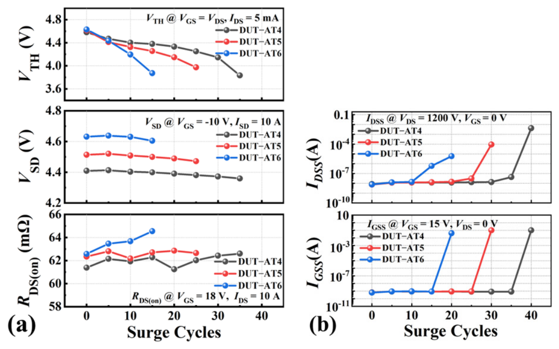
The degradation trends of the electrical parameters with the surge cycles are shown in Figure 9. Prior to complete failure, DUT-AT4, AT5, and AT6 exhibit significant degradation in VTH as the surge cycles increase, where the degradation is fastest at VGS = −10 V, consistent with the single surge stress result. RDS(on) increases by 1.9%, 0.5%, and 5.16% for AT4, AT5, and AT6, respectively, while the changes in VSD remain below 1%. IGSS of DUT-AT4, AT5, and AT6 escalates to the mA range when the devices fail, confirming the inevitable damage to the gate oxide layer. However, only DUT-AT4’s IDSS reaches the mA level, losing its blocking capability.
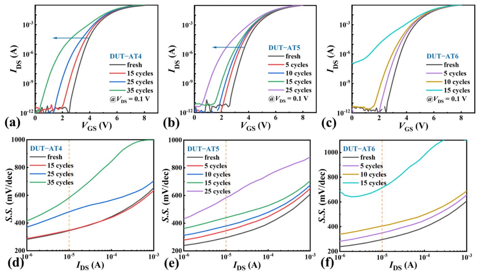
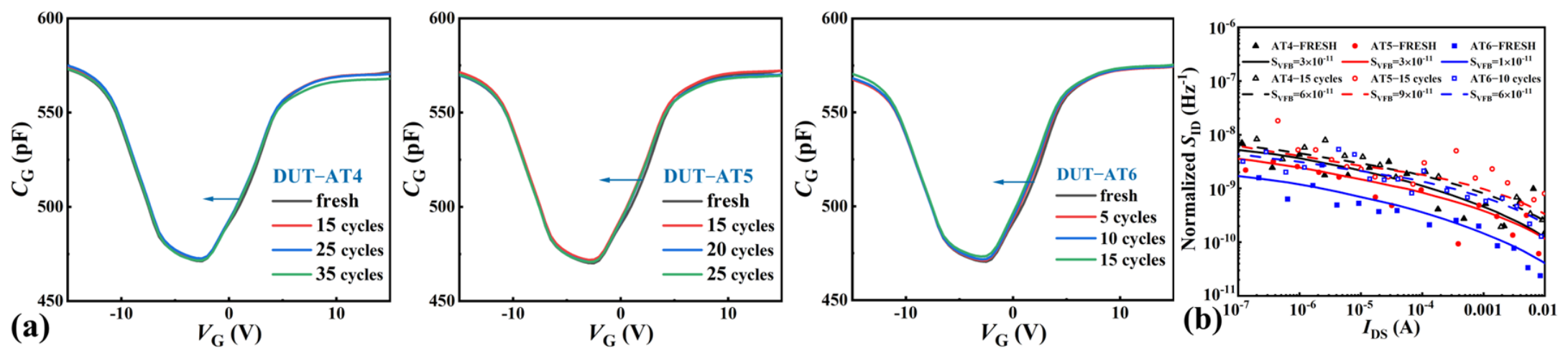
In Figure 10, the transfer characteristics of the DUTs shift to the left with the increasing surge stress cycles; meanwhile, the S.S. increases as the surge cycles increase. The degradation trend of DUT-AT6 is the most pronounced, demonstrating that VGS significantly influences the stability of the gate–oxide interface. Figure 11a illustrates the degradation trends of the Cg-Vg characteristics of the DUTs. As the applied VGS becomes more negative, the negative shift in the Cg-Vg curves within the 0 V to 5 V range of Vg intensifies, indicating more trap generation in the gate oxide layer, consistent with the results of VTH. Figure 11b reveals that the low-frequency noise power spectral density of DUT-AT4, AT5, and AT6 after surge stress is 2, 3, and 6 times greater than the initial values, respectively, consistent with the Cg-Vg results. It is shown that the larger negative bias may amplify the generation of defects, consistent with the results for the single surge test.

3.3. Repetitive Surge Test at 60% SSCmax

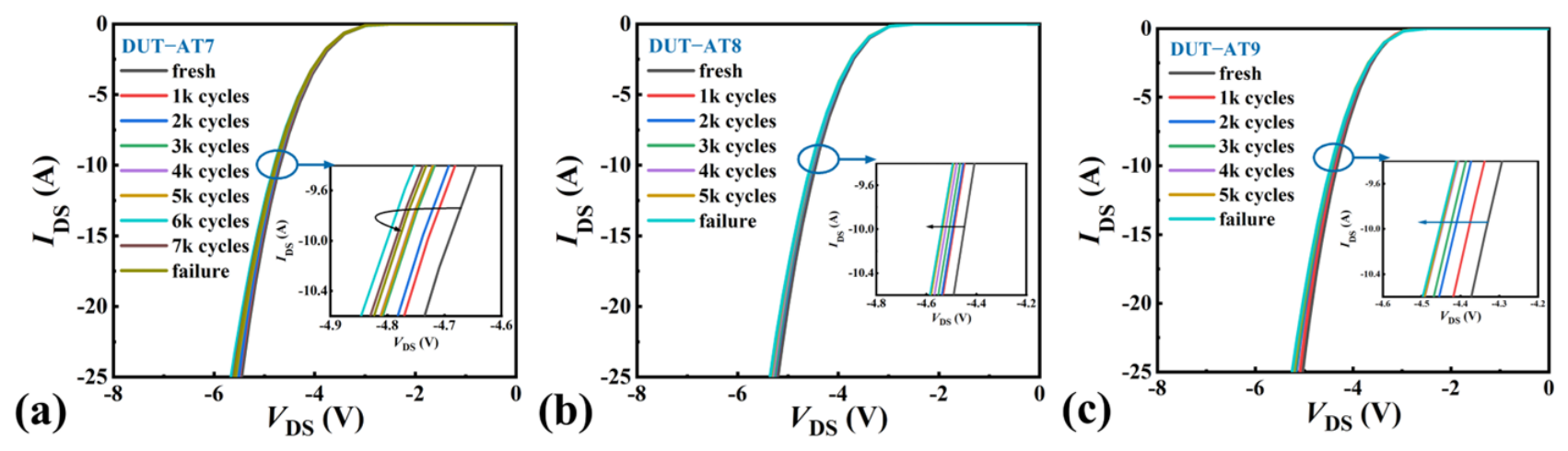
VGS for DUT-AT7, AT8, and AT9 are set at 0 V, −5 V, and −10 V, respectively, with a repetitive surge current of 90 A, corresponding to 60% of the maximum single surge current. The maximum surge cycles to failure and three-terminal resistances when the DUTs fail are presented in Table 5. The surge endurance of DUT-AT7, AT8, and AT9 is in the range of thousands of cycles, which is hundreds of times that for 90% SSCmax. This may be caused by the decrease in the surge current amplitude. The resistances between the gate and source terminals of the devices decrease to the kilohm (kΩ) range, indicating the presence of a leakage path between the gate and source, which is consistent with the 90% SSCmax test results. For DUT-AT7, the resistances between the drain-gate and source-drain terminals decrease to the tens of megohms (MΩ) range, yet the device still retains its blocking capability. Unlike the case of the large surge current stress, the variation trends of the third-quadrant characteristics under small surge current stress show no significant dependence on VGS, as shown in Figure 12. The knee voltage and forward voltage drop of the body diode exhibit a gradually degrading trend.
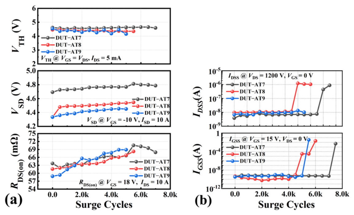
As shown in Figure 13, after the devices withstand small surge current stress, DUT-AT7, AT8, and AT9 have failed after 7000, 5500, and 5000 surge cycles, respectively. The degradation in VTH is relatively slow, while the changes in RDS(on) and VSD are more pronounced compared with those for 90% SSCmax. The IGSS of DUT-AT7 and AT8 increase to the mA range, and IDSS increases to the microampere (µA) range when failure occurs. However, DUT-AT9’s IDSS remains unchanged.
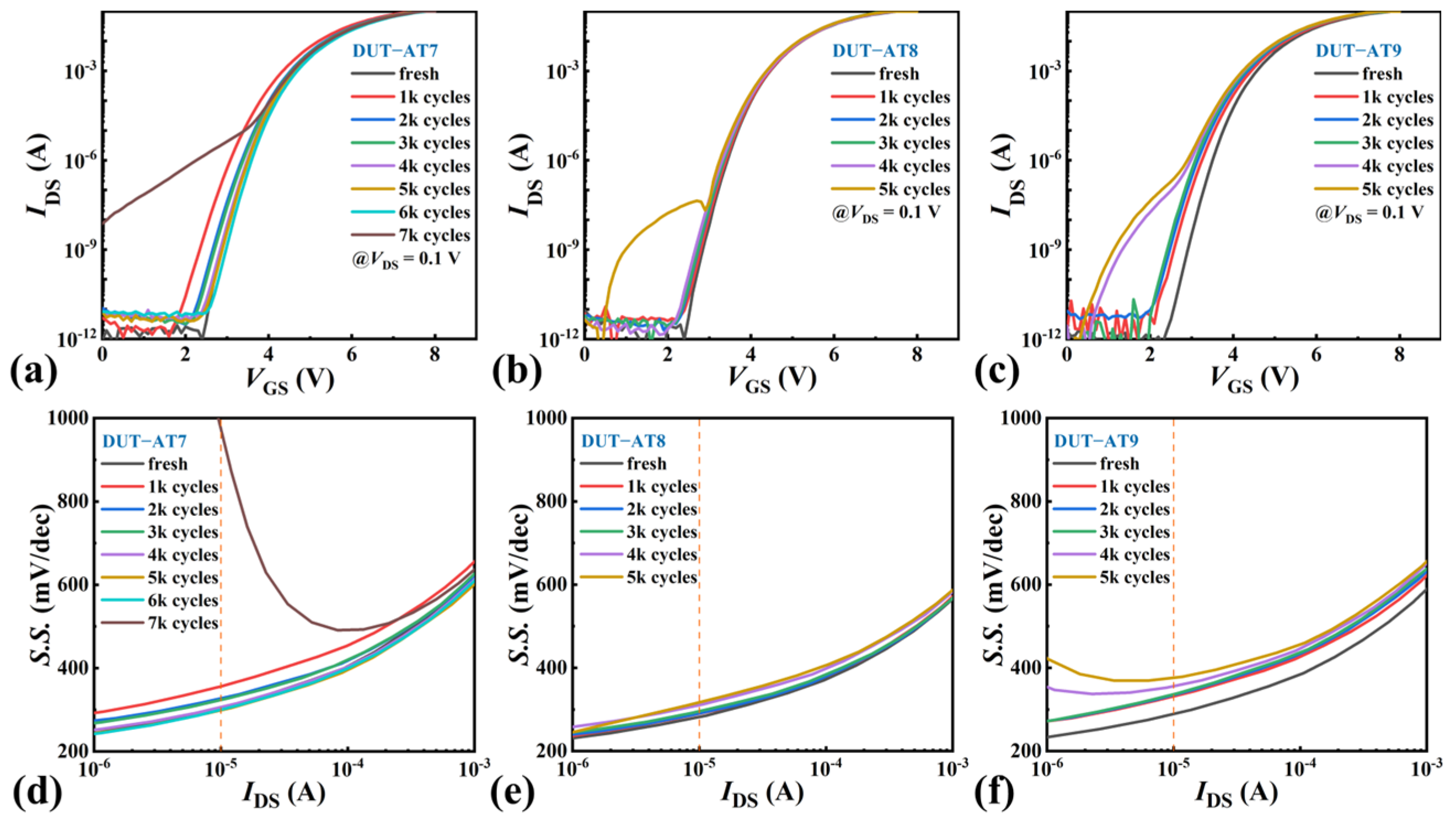
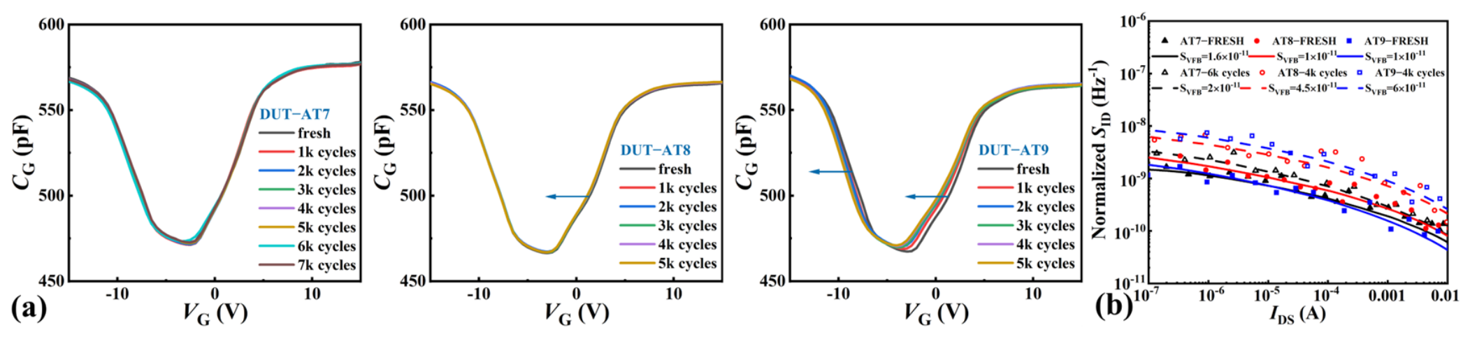
In agreement with the degradation trend under large current repetitive surge stress, the VTH degradation (Figure 13), transfer characteristics and S.S. (Figure 14), Cg-Vg characteristics, and LFN characteristics (Figure 15a,b) of the tested devices all exhibit a consistent trend. This indicates that more negative VGS leads to more defect generation in the gate oxide layer, which results in more obvious VTH degradation during the repetitive surge test at 60% SSCmax.

4. Failure Mechanism Analysis

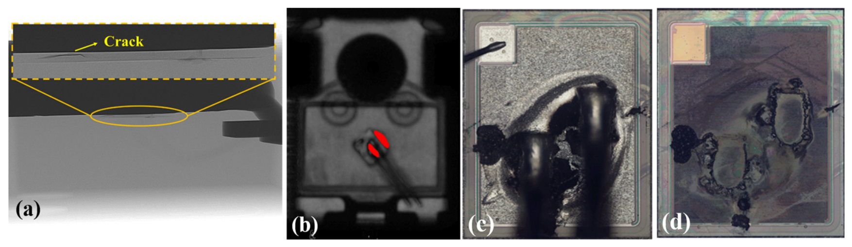
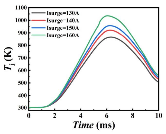
To study the failure mechanisms of AT SiC MOSFETs for single and repetitive surge current stress, failure analyses for DUT-AT3, AT6, and AT9 have been conducted, respectively. The X-ray inspection results for DUT-AT3 are shown in Figure 16a, where cracks are observed on the chip layer. Figure 16b displays the front-side SAM results, indicating delamination between the chip layer and the surrounding molding compound of DUT-AT3 after single surge stress. This is caused by the device temperature rising rapidly under single surge current stress, generating thermomechanical stress that causes structural changes in the overheated packaging material, corroborating the proposed failure physics in prior studies [31]. After decapsulation of the device, significant burn marks and cracks are observed near the source metal and around the gate bar, as shown in Figure 16c,d. The estimated junction temperatures are shown in Figure 17. For DUT-AT3, the localized junction temperature spiking is caused by the surge current of 160 A exceeding the melting point of Al (933 K), and the temperature rise accelerates the dielectric/interface degradation and leakage current increase. The abrupt increase in IDSS and IGSS near failure may then further enhance local power dissipation, forming positive electro-thermal feedback, consistent with the literature [15]. In contrast, when the surge current is below 140 A, the device junction temperature remains below the melting point of Al, which provides further evidence that repetitive surges induce cumulative degradation.
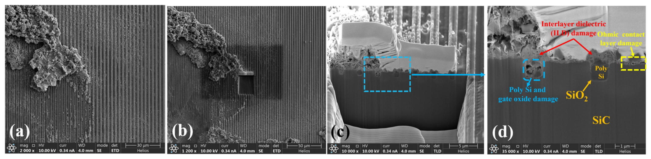
To further investigate the failure mechanism, focused ion beam (FIB) milling is performed on the area near the source metal burnout for DUT-AT3. As shown in Figure 18d, the melted source Al metal erodes and penetrates through the interlayer dielectric (ILD), which leads to the short circuit between the gate and the source. Meanwhile, the melted Al fills and breaks through the ohmic contact layer between the source metal and SiC doped region, which results in the degradation of the blocking capability. Both aforementioned factors ultimately lead to a three-terminal short circuit, which is consistent with the published literature [32,33].
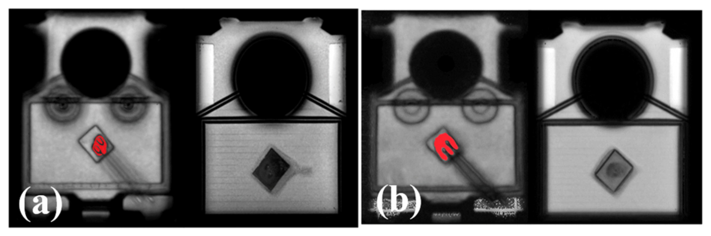
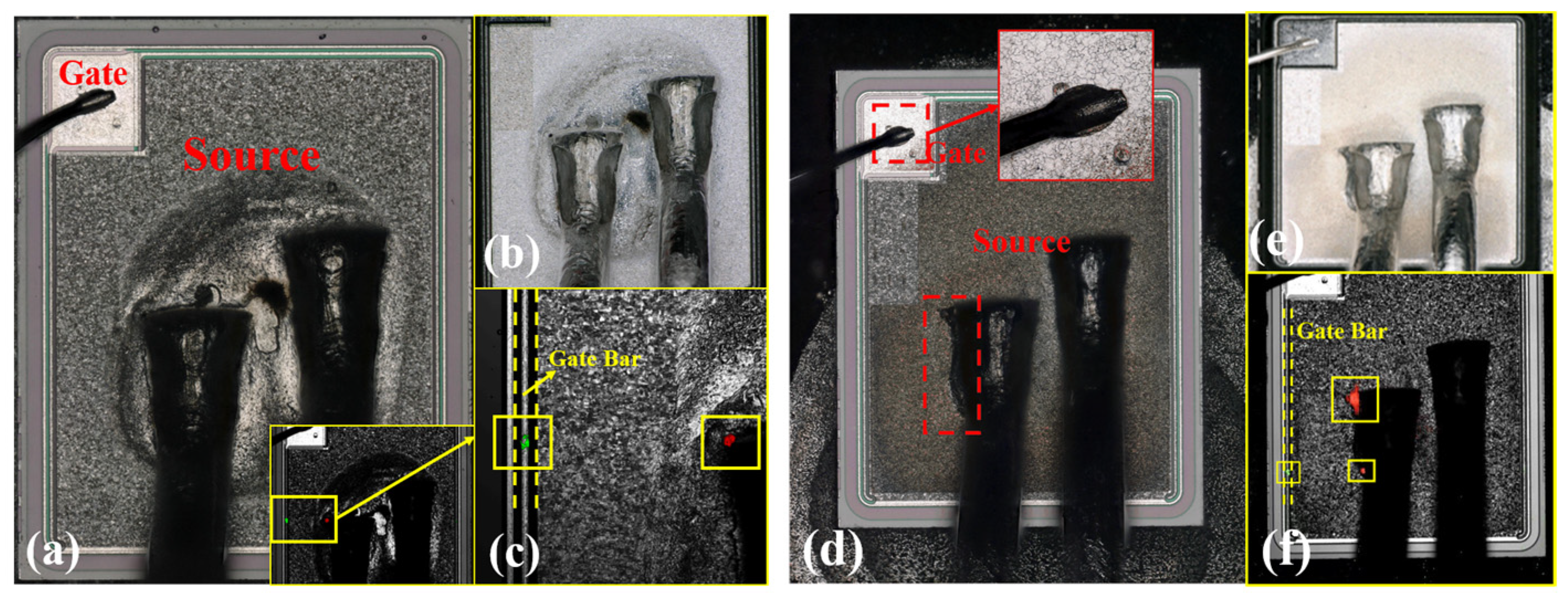
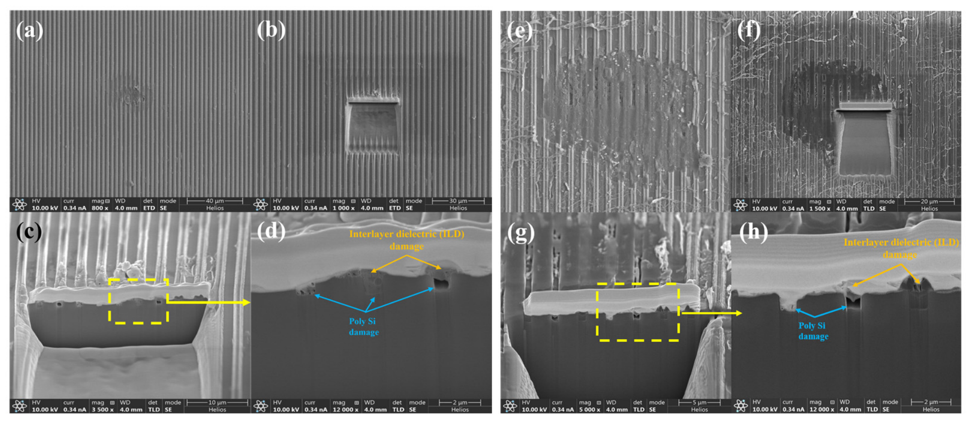
As shown in Figure 19, the SAM inspection results for DUT-AT6 and AT9 identify damage near the source bonding wires, accompanied by delamination of the encapsulant material (the red region). After the decapsulation of the devices, chip surface damage is observed by using a metallurgical microscope, as shown in Figure 19. Blackened carbonized marks are observed near the source bonding wires for DUT-AT6 and AT9, while no cracks are found on the chip surface. The severity of the burns for both DUT-AT6 and AT9 is lower than that of DUT-AT3, with the fewest burn marks for DUT-AT9. Further, leakage defect localization is performed by using the OBIRCH mode of emission microscopy (EMMI), as illustrated in Figure 20c,f. The red light indicates leakage locations, while the green light highlights impedance anomaly points. The green spot is located at the gate bar of the chip edge, while the red spot is located near the active region of the bond wires, and further FIB milling is conducted near the active region bond wire, followed by SEM scanning. As shown in Figure 21d,h, similar failure mechanisms have been observed for DUT-AT6 and AT9. The melted Al metal penetrates through the ILD and eventually leads to the short circuit between the gate and the source after repetitive surge current stress. Different from that of single surge current stress, the ohmic contact layer remains intact without obvious damage.
The device’s lifetime and failure mechanisms are intrinsically linked to its structural characteristics during the surge stress test. During third-quadrant surge operation, the current is shared by the intrinsic body diode and the MOS-channel-assisted conduction path. The asymmetric trench layout and the deep p+ shielding region are beneficial for reducing the on-state resistance and protecting the trench-bottom oxide under normal operation. However, during high surge current stress, these structural features also affect the internal current distribution. Since the body-diode path dominates (as shown in Figure 3c), the surge current mainly flows through deep p+ shielding region/n-drift junction system. Due to the asymmetric cell geometry, current crowding may occur near the trench sidewall in the deep p+ shielding corner [34]. Such nonuniform current distribution can result in localized Joule heating and enhanced electrothermal stress near the SiC/SiO2 interface, thereby accelerating interface-state generation, oxide-related degradation, and leakage current increase under repetitive surge stress.
Increasing the channel current contribution reduces the body-diode current component, lowers the effective VSD, and decreases the surge energy dissipated in the bipolar diode path. Therefore, the localized heating and carrier-injection-induced degradation around the body diode and deep p+ shielding region can be mitigated. This means a larger channel current contribution at VGS = 0 V is beneficial for improving repetitive surge reliability.

5. Conclusions

The reliability of asymmetric trench-gate SiC MOSFETs under single and repetitive surge current stresses (90% SSCmax and 60% SSCmax) at different gate bias voltages (VGS = 0 V, −5 V, and −10 V) has been systematically investigated.
When the device undergoes single surge current stress, it is indicated that VGS does not affect the surge capability of the DUTs, with the same maximum surge current of 150 A. However, VGS has influenced the degradation of key parameters. As VGS becomes more negative, the degradation of VTH becomes more obvious, with a decrease of up to 33.34% for AT3. This may be the result of a more negative VGS leading to the increase in SiC/SiO2 interface defect density, intensifying gate-oxide deterioration, which is verified by the results of the transfer characteristics, S.S., Cg-Vg characteristics, and LFN characteristics. It is indicated from the microscopic analysis that the failure mode involves both chip failure and package failure. This is attributed to thermal runaway caused by a large single surge current, which leads to the melted source Al metal penetrating through the interlayer dielectric and the ohmic contact layer between the source metal and the SiC-doped region, respectively. It results in not only the short circuit between the gate and the source but also degradation in the blocking capability, ultimately leading to a three-terminal short circuit.
Different from a single surge current, it is indicated that VGS has a significant impact on surge capability from the results of the large current (90% SSCmax) repetitive surge stress. When VGS = 0 V, the devices can withstand the maximum number of surge cycles with the least parameter degradation. The number of surge cycles the devices can withstand decreases as VGS becomes more negative. This may be caused by a weaker contribution of the channel-assisted leakage conduction during repetitive current stress. As with the single surge stress, both chip and package failure occur for the large current (90% SSCmax) repetitive surge stress. The device failure is caused by the melted Al metal penetrating through the interlayer dielectric and eventually leading to the short circuit between the gate and the source after repetitive surge current stress. Different from that of single surge current stress, the ohmic contact layer remains intact without obvious damage.
Compared with large surge current stress, the device can withstand several hundred times more surge cycles under small current (60% SSCmax) repetitive surge stress. The maximum cycles are still observed at VGS = 0 V, with a downward trend as VGS becomes more negative. The failure mode and mechanism remain consistent with the large surge current repetitive tests.
To enhance the surge reliability of asymmetric trench-type SiC MOSFETs, it is recommended to increase the proportion of channel current in the total surge current, which reduces conduction losses and mitigates thermal runaway risks. Therefore, it is advised to operate such devices at VGS = 0 V in the third quadrant.

Author Contributions

Conceptualization, M.Y. and Z.W.; methodology, D.C. and Z.W.; investigation, M.Y., Y.L. (Yuncong Li), and Y.Z.; resources, H.X. and Z.W.; data curation, M.Y. and Y.Z.; writing—original draft preparation, M.Y.; writing—review and editing, M.Y. and Z.W.; supervision, D.C., Z.W., and Y.L. (Yuansheng Li); project administration, J.L.; funding acquisition, Z.W. All authors have read and agreed to the published version of the manuscript.

Funding

This work was funded by Guangdong S&T Programme (grant no. 2022B0701180002), National Natural Science Foundation of China (NSFC) (grant no. 62574062), Guangdong Basic and Applied Basic Research Foundation (grant no. 2024A1515010758), and the Opening Project of State Key Laboratory of Reliability Technology for Electronic Components (grant no. 25D04).

Informed Consent Statement

Not applicable.

Data Availability Statement

The data presented in this study are available upon request from the corresponding author.

Conflicts of Interest

The authors declare no conflicts of interest.

References

  1. Abdelaleem, A.; Monfared, M.; Jennings, M.; Jahdi, S.; Karout, M.A.; Nel, B.; Evans, J.; Fisher, C.A. SiC MOSFET reliability: Review of degradation mechanisms, failures, and enhancement strategies. E-Prime–Nexus Electr. Electron. Intell. Eng. 2026, 17, 201163. [Google Scholar] [CrossRef] [Scilit]
  2. Avraham, T.; Dhyani, M.; Bernstein, J.B. Reliability Challenges, Models, and Physics of Silicon Carbide and Gallium Nitride Power Devices. Energies 2025, 18, 1046. [Google Scholar] [CrossRef] [Scilit]
  3. Wei, J.; Wei, Z.; Fu, H.; Cao, J.; Wu, T.; Sun, J.; Zhu, X.; Li, S.; Zhang, L.; Liu, S.; et al. Review on the Reliability Mechanisms of SiC Power MOSFETs: A Comparison Between Planar-Gate and Trench-Gate Structures. IEEE Trans. Power Electron. 2023, 38, 8990–9005. [Google Scholar] [CrossRef] [Scilit]
  4. Peters, D.; Basler, T.; Zippelius, B.; Aichinger, T.; Bergner, W.; Esteve, R. The New CoolSiC™ Trench MOSFET Technology for Low Gate Oxide Stress and High Performance. In Proceedings of the PCIM Europe 2017; International Exhibition and Conference for Power Electronics, Intelligent Motion, Renewable Energy and Energy Management, Nuremberg, Germany, 16–18 May 2017; pp. 1–7. [Google Scholar]
  5. Puschkarsky, K.; Grasser, T.; Aichinger, T.; Gustin, W.; Reisinger, H. Review on SiC MOSFETs High-Voltage Device Reliability Focusing on Threshold Voltage Instability. IEEE Trans. Electron Devices 2019, 66, 4604–4616. [Google Scholar] [CrossRef] [Scilit]
  6. Sadik, D.-P.; Heinig, S.; Jacobs, K.; Johannesson, D.; Lim, J.-K.; Nawaz, M.; Dijkhuizen, F.; Bakowski, M.; Norrga, S.; Nee, H.-P. Investigation of the surge current capability of the body diode of SiC MOSFETs for HVDC applications. In Proceedings of the 2016 18th European Conference on Power Electronics and Applications (EPE’16 ECCE Europe), Karlsruhe, Germany, 5–9 September 2016; pp. 1–10. [Google Scholar]
  7. Yang, J.; Jahdi, S.; Stark, B.; Alatise, O.; Ortiz-Gonzalez, J.; Mellor, P. Analysis of the 1st and 3rd Quadrant Transients of Symmetrical and Asymmetrical Double-Trench SiC Power MOSFETs. IEEE Open J. Power Electron. 2021, 2, 265–276. [Google Scholar] [CrossRef] [Scilit]
  8. Jiang, X.; Wang, J.; Chen, J.; Li, Z.; Zhai, D.; Yang, X.; Ji, B.; Shen, Z.J. Investigation on Degradation of SiC MOSFET Under Surge Current Stress of Body Diode. IEEE J. Emerg. Sel. Top. Power Electron. 2020, 8, 77–89. [Google Scholar] [CrossRef] [Scilit]
  9. Fang, S.; Li, K.; Tang, Y.; Zhong, Y.; Tang, S.; Wang, Z. Research on Surge Current and Avalanche Voltage Reliability Testing of 1200V SiC MOSFETs. In Proceedings of the 2025 26th International Conference on Electronic Packaging Technology (ICEPT), Shanghai, China, 5–7 August 2025; pp. 1–5. [Google Scholar]
  10. Ma, D.; He, Z.; Chen, Y.; Shi, Y.; Wang, J.; Yang, C.; Zhang, M.; Shen, Y.; He, L.; Lu, G.; et al. Degradation Evaluation and Defects Analysis for 1.2-kV Planar-Gate SiC MOSFETs Under Repetitive Surge Current Stress. IEEE Trans. Electron Devices 2023, 70, 6473–6479. [Google Scholar] [CrossRef] [Scilit]
  11. Xu, H.; Ren, N.; Zhu, Z.; Wu, J.; Liu, L.; Guo, Q.; Sheng, K. Methodology for Enhanced Surge Robustness of 1.2-kV SiC MOSFET Body Diode. IEEE J. Emerg. Sel. Top. Power Electron. 2022, 10, 5039–5047. [Google Scholar] [CrossRef] [Scilit]
  12. Guan, H.; Chang, Y.; Cao, J.; Kong, L.; Liu, P. Simulation, Verification, and Failure Analysis of 1.2kV Planar-Gate SiC MOSFET Under Surge Current Stress of Body Diode. In Proceedings of the 2025 26th International Conference on Electronic Packaging Technology (ICEPT), Shanghai, China, 5–7 August 2025; pp. 1–6. [Google Scholar]
  13. Wang, N.; Zhang, J.; Zhang, Y.; Xu, S.; Deng, F. Evaluation of Silicon Carbide Power MOSFET on Third-quadrant Surge Current Performance. In Proceedings of the IECON 2025–51st Annual Conference of the IEEE Industrial Electronics Society, Madrid, Spain, 14–17 October 2025; pp. 1–6. [Google Scholar]
  14. Liang, B.; Cui, X.; Zheng, F.; Li, X.; Li, H.; Chen, Z.; Jin, R.; Tang, X. Surge Characteristics of Planar-Gate Silicon Carbide MOSFET in the Third Quadrant. IEEE Trans. Power Electron. 2025, 40, 10635–10648. [Google Scholar] [CrossRef] [Scilit]
  15. Li, H.; Wang, J.; Ren, N.; Xu, H.; Sheng, K. Investigation of 1200 V SiC MOSFETs’ Surge Reliability. Micromachines 2019, 10, 485. [Google Scholar] [CrossRef] [Scilit] [PubMed]
  16. Zhan, X.; He, Y.; Jiang, X.; Yuan, H.; Song, Q.; Tang, X.; Gong, X.; Zhang, Y. Investigation of SiC MOSFET Structures for Surge Robustness in the Third Quadrant Under Various VGS Biases. IEEE Open J. Power Electron. 2025, 6, 1028–1035. [Google Scholar] [CrossRef] [Scilit]
  17. Xiang, Z.; Luo, T.; Wang, W.; Sun, B.; Sun, B.; Zhang, Q.; Zhang, G.; Fan, J. Package-Level Electro-Thermal Simulation With Transient Thermal Resistance Model for Surge Stress Failure Analysis of SiC MOSFET. IEEE Trans. Device Mater. Reliab. 2026, 26, 42–53. [Google Scholar] [CrossRef] [Scilit]
  18. Zhan, X.; He, Y.; Lai, J.; Yuan, H.; Song, Q.; Tang, X.; Gong, X.; Zhang, Y. Investigation on Degradation of 1200-V Planar and Trench SiC MOSFET Under Surge Current Stress of Body Diode. IEEE Trans. Electron Devices 2024, 71, 709–714. [Google Scholar] [CrossRef] [Scilit]
  19. Zhu, Z.; Xu, H.; Liu, L.; Ren, N.; Sheng, K. Investigation on Surge Current Capability of 4H-SiC Trench-Gate MOSFETs in Third Quadrant Under Various VGS Biases. IEEE J. Emerg. Sel. Top. Power Electron. 2021, 9, 6361–6369. [Google Scholar] [CrossRef] [Scilit]
  20. Guan, H.; Chang, Y.; Bai, P.; Bian, L.; Zhang, Q.J.; Liu, P. Investigation of Degradation Mechanism in 1200-V SiC MOSFETs Under Surge Current Stress of Body Diode Using Electro-Thermal-Mechanical Analysis. IEEE J. Emerg. Sel. Top. Power Electron. 2026, 14, 3278–3288. [Google Scholar] [CrossRef] [Scilit]
  21. JEP183A; Guidelines for Measuring the Threshold Voltage (VT) of SiC MOSFETs. JEDEC Solid State Technology Association: Arlington, VA, USA, 2023.
  22. Pala, V.; Van Brunt, E.; Ryu, S.; Hull, B.; Allen, S.; Palmour, J.; Hefner, A. Physics of bipolar, unipolar and intermediate conduction modes in Silicon Carbide MOSFET body diodes. In Proceedings of the 2016 28th International Symposium on Power Semiconductor Devices and ICs (ISPSD), Prague, Czech Republic, 12–16 June 2016; pp. 227–230. [Google Scholar]
  23. Zhang, M.; Li, H.; Yang, Z.; Zhao, S.; Wang, X.; Ding, L. Surge Current Distribution in Paralleled SiC MOSFETs Under Third-Quadrant Operation. IEEE Trans. Power Electron. 2025, 40, 3077–3089. [Google Scholar] [CrossRef] [Scilit]
  24. Siemieniec, R.; Peters, D.; Esteve, R.; Bergner, W.; Kück, D.; Aichinger, T.; Basler, T.; Zippelius, B. A SiC Trench MOSFET concept offering improved channel mobility and high reliability. In Proceedings of the 2017 19th European Conference on Power Electronics and Applications (EPE’17 ECCE Europe), Warsaw, Poland, 11–14 September 2017; pp. 1–13. [Google Scholar]
  25. Maresca, L.; Matacena, I.; Riccio, M.; Irace, A.; Breglio, G.; Daliento, S. Influence of the SiC/SiO2SiC MOSFET Interface Traps Distribution onC–VMeasuremnts Evaluated by TCAD Simulations. IEEE J. Emerg. Sel. Top. Power Electron. 2021, 9, 2171–2179. [Google Scholar] [CrossRef] [Scilit]
  26. Ding, X.; Zhao, Y.; Yang, Y. Characterization of Low-Temperature for SiC MOSFET Based On the Capacitance-Voltage Characteristic. In Proceedings of the 2022 IEEE Transportation Electrification Conference and Expo, Asia-Pacific (ITEC Asia-Pacific), Haining, China, 28–31 October 2022; pp. 1–5. [Google Scholar]
  27. Yang, X.; Wang, X.; Li, Q.; Liu, Y.; Sun, Y.; Liu, G. An Accurate Datasheet-Driven Analytical Model of SiC MOSFET Incorporating Stage-Dominant Cgs(Vgs, Vds) and Cgd(Vgs, Vds). IEEE Trans. Power Electron. 2026, 41, 14579–14595. [Google Scholar] [CrossRef] [Scilit]
  28. Asanovski, R.; Palestri, P.; Selmi, L. On the accuracy of the formula used to extract trap density in MOSFETs from 1/f noise. Solid-State Electron. 2022, 194, 108311. [Google Scholar] [CrossRef] [Scilit]
  29. Yang, X.; Chen, Y.Q.; Hou, B.; Xu, X.; Wang, J.; Huang, Y.; Chen, Q.; Zhou, C. Degradation Behavior and Defect Analysis for SiC Power MOSFETs Based on Low-Frequency Noise Under Repetitive Power-Cycling Stress. IEEE Trans. Electron Devices 2021, 68, 666–671. [Google Scholar] [CrossRef] [Scilit]
  30. Cheng, Z.; Sang, L.; He, F.; He, Y.; Li, Z.; Jin, R.; Cui, P. Investigation on Degradation of Switching Characteristics in SiC MOSFETs Under Repetitive Surge Current. Electronics 2026, 15, 2721. [Google Scholar] [CrossRef] [Scilit]
  31. Xu, S.; Li, X.; Zhao, H.; Wen, Y.; Peng, W.; Zhou, Z.; Li, X.; Deng, X.; Zhang, B. A novel mechanical stress related failure mechanism of the state-of-the-art SiC double trench MOSFET under surge current stress. In Proceedings of the 2025 IEEE Workshop on Wide Bandgap Power Devices and Applications in Asia (WiPDA Asia), Beijing, China, 15–17 August 2025; pp. 1–4. [Google Scholar]
  32. Peng, J.; Sun, P.; Cai, Y.; Zhang, H.; Zhao, Z. Study on the Blocking Capability Decreasing of SiC MOSFET After Short-Circuit Gate-Source Failure. In Proceedings of the 16th Annual Conference of China Electrotechnical Society; Springer Nature: Singapore, 2022. [Google Scholar]
  33. Zhang, Z.; Liang, L.; Shang, H. Review of SiC MOSFET Failure Analysis Under Extreme Conditions: High Temperature, High Frequency and Irradiation. In Proceedings of the Conference Proceedings of 2021 International Joint Conference on Energy, Electrical and Power Engineering; Springer Nature: Singapore, 2022. [Google Scholar]
  34. He, L.; Zhang, M.; Li, C.; Niu, H.; Shi, Y.; Chen, X.; Fang, S.; Wang, Z.; Chen, Y. Comparative Investigation on Device-Level Failure of Three Typical SiC MOSFETs Under Single Surge Current Stress. IEEE Trans. Power Electron. 2026, 1–11, Early Access. [Google Scholar] [CrossRef] [Scilit]
Figure 1. AT-MOSFET: (a) structural diagram and (b) cross-sectional view.
Micromachines 17 00823 g001
Figure 2. (a) Simplified schematic of the surge current test circuit. (b) Surge test platform for the SiC MOSFETs.
Micromachines 17 00823 g002
Figure 3. (a) Body diode characteristic curves of the DUTs at different gate voltages. (b) The surge current path for VGS between −9 V and 0 V. (c) Variation in the channel current proportion with VSD under different VGS.
Micromachines 17 00823 g003
Figure 4. Single surge current waveforms and surge trajectories of the DUTs under different gate voltages: (a,d) DUT-AT1, (b,e) DUT-AT2, and (c,f) DUT-AT3.
Micromachines 17 00823 g004
Figure 5. Degradation of electrical parameters for DUT-AT1, AT2, and AT3 at varying VGS: (a) VTH, VSD, RDS(on), and (b) IDSS, IGSS.
Micromachines 17 00823 g005
Figure 6. Cg-Vg characteristics for DUT-AT1, AT2, and AT3.
Micromachines 17 00823 g006
Figure 7. Degradation of (a) subthreshold swing and (b) normalized noise power spectral density for DUT-AT1, AT2, and AT3.
Micromachines 17 00823 g007
Figure 8. Degradation in the third-quadrant characteristics of the DUTs under repetitive surge current stress of 90% SSCmax: (a) DUT-AT4, (b) DUT-AT5, and (c) DUT-AT6.
Micromachines 17 00823 g008
Figure 9. Degradation of electrical parameters for DUT-AT4, AT5, and AT6 at varying VGS: (a) VTH, VSD, RDS(on) and (b) IDSS, IGSS.
Micromachines 17 00823 g009
Figure 10. Degradation of the transfer curves and subthreshold swing for the DUTs during the repetitive surge current test: (a,d) DUT-AT4, (b,e) DUT-AT5, and (c,f) DUT-AT6.
Micromachines 17 00823 g010
Figure 11. (a) Cg-Vg characteristics for DUT-AT4, AT5, and AT6. (b) Degradation of the normalized noise power spectral density for DUT-AT4, AT5, and AT6.
Micromachines 17 00823 g011
Figure 12. Degradation in the third-quadrant characteristics of the DUTs under repetitive surge current stress of 60% SSCmax: (a) DUT-AT7, (b) DUT-AT8, and (c) DUT-AT9.
Micromachines 17 00823 g012
Figure 13. Degradation of electrical parameters for DUT-AT7, AT8, and AT9: (a) VTH, VSD, RDS(on) and (b) IDSS, IGSS.
Micromachines 17 00823 g013
Figure 14. Degradation of the transfer curves and subthreshold swing for the DUTs during the repetitive surge current test of 60% SSCmax: (a,d) DUT-AT7, (b,e) DUT-AT8, and (c,f) DUT-AT9.
Micromachines 17 00823 g014
Figure 15. (a) Cg-Vg characteristic and (b) degradation of normalized noise power spectral density for DUT-AT7, AT8, and AT9.
Micromachines 17 00823 g015
Figure 16. DUT-AT3: (a) X-ray inspection result. (b) SAM inspection result. (c) Surface morphology after decapsulation and before Al removal. (d) Surface morphology after decapsulation and Al removal.
Micromachines 17 00823 g016
Figure 17. Estimated transient junction temperature of DUT-AT3 at different surge currents.
Micromachines 17 00823 g017
Figure 18. FIB-SEM analysis of failed DUT-AT3: (a,b) dye surface morphology and (c,d) a cross-section view of the damaged cell structure.
Micromachines 17 00823 g018
Figure 19. SAM inspection results of the DUTs: (a) DUT-AT6 and (b) DUT-AT9.
Micromachines 17 00823 g019
Figure 20. (a,b) Decapsulated chip surfaces and (c) OBIRCH localization of DUT-AT6. (d,e) Decapsulated chip surfaces and (f) OBIRCH localization of DUT-AT9.
Micromachines 17 00823 g020
Figure 21. FIB-SEM analysis results: (a,b) dye surface morphology of DUT-AT6, (c,d) a cross-section view of the damaged cell structure of DUT-AT6, (e,f) dye surface morphology of DUT-AT9, and (g,h) a cross-section view of the damaged cell structure of DUT-AT9.
Micromachines 17 00823 g021
Table 1. Rated parameters and test conditions of the DUTs.
Vrated (V)Irated (A)VGS (V)Surge Modes
Single-PulseRepetitive
(90% SSCmax)
Repetitive
(60% SSCmax)
1200360AT1AT4AT7
−5AT2AT5AT8
−10AT3AT6AT9
Table 2. Estimated parameters under different VGS bias conditions.
VGS (V)Measured SSCmax (A)VSD at Same ISD (V)Epluse (J)Estimated Tj (K)
−101507.144.75949.7
−56.984.66933.3
07.244.81959.2
Table 3. Surge capability and three-terminal resistances when the DUTs fail.
DUTsIFSM (A)Surge
Capability
RGS (Ω)RSG (Ω)RDG (Ω)RGD (Ω)RDS (Ω)RSD (Ω)
AT1 1604.4425240.20.225.425.4
AT2 23.223.21.2 k1.1 k1.1 k1.2 k
AT3191910102020
Table 4. The maximum surge cycles and three-terminal resistances when the devices fail (90% SSCmax).
DUTsIsurge (A)CyclesRGS (Ω)RSG (Ω)RDG (Ω)RGD (Ω)RDS (Ω)RSD (Ω)
AT41354047.347.20.6 M1.5 M1.5 M0.6 M
AT530108.9108.914.5 M--15.1 M
AT6201.1 k1.1 k----
Table 5. The maximum surge cycles and three-terminal resistances when the devices fail (60% SSCmax).
DUTsIsurge (A)CyclesRGS (Ω)RSG (Ω)RDG (Ω)RGD (Ω)RDS (Ω)RSD (Ω)
AT7 9075003.1 k3.1 k20.9 M--21.1 M
AT8 60001.1 k1.1 k----
AT9 55000.7 k0.7 k----
Disclaimer/Publisher’s Note: The statements, opinions and data contained in all publications are solely those of the individual author(s) and contributor(s) and not of MDPI and/or the editor(s). MDPI and/or the editor(s) disclaim responsibility for any injury to people or property resulting from any ideas, methods, instructions or products referred to in the content.