1. Introduction
Static frequency dividers are key building blocks in millimeter-wave frequency generation systems. Driven by broadband communication, satellite links, and high-speed instrumentation, they are required to provide wide operating bandwidth, high input frequency, stable phase noise, and sufficient input power tolerance [
1,
2,
3].
Emitter-coupled logic (ECL) and current-mode logic (CML) structures are widely adopted for high-speed static dividers due to their fast switching speed and good noise immunity [
4,
5,
6]. In these dividers, the maximum operating frequency is mainly limited by the switching speed of the master–slave latch core. To extend the operating frequency, circuit-level techniques, such as inductive peaking, asymmetric latch, split-load structures, and
fT-doubler topologies, have been reported [
7,
8,
9,
10]. In parallel, InP HBT/DHBT technologies are attractive for millimeter-wave and sub-terahertz dividers due to their high transition frequency and high breakdown voltage, while SiGe BiCMOS offers advantages in power efficiency, integration, and cost [
11,
12,
13].
Despite recent progress, wideband high-frequency division with low implementation overhead remains difficult to achieve. Advanced InP HBT/DHBT technologies can support very high operating frequencies; for instance, a 0.25-μm InP HBT static divider has achieved operation up to 204.8 GHz, but with a DC power consumption of 1820 mW [
11]. Circuit-level speed-enhancement techniques, such as
fT-doubler topologies, can further extend the operating range, but usually at the cost of increased latch complexity and layout difficulty [
10]. SiGe BiCMOS dividers offer good power efficiency and integration advantages, yet their lower breakdown voltage may restrict the allowable input power range [
12]. Meanwhile, mature 0.7-μm InP DHBT platforms provide robust breakdown characteristics and fabrication maturity, but their high-frequency capability still requires improvement. These trade-offs motivate a practical optimization strategy that enhances static divider performance on mature InP DHBT platforms without full process migration or major topology modification.
In this work, such an optimization is achieved by selectively introducing 0.5 μm high-fT DHBTs into only the speed-critical switching and latching pairs of a CML master–slave core, while retaining standard 0.7 μm devices in the remaining circuits. This mixed-device strategy reduces core parasitic capacitances and extends the operating bandwidth with limited circuit and process overhead. Based on this approach, a static 1:2 frequency divider is implemented in a commercial 0.7 μm InGaAs/InP DHBT technology, achieving a continuous operating range of 0.5–67 GHz, a full-band input power range of −5 to +10 dBm, and an SSB phase noise of −141.03 dBc/Hz at 100 kHz offset with a 30 GHz input.
2. Process and Device Selection
The divider is fabricated on a commercial 0.7 μm InGaAs/InP DHBT process, Nanjing Electronic Devices Institute, Nanjing, China. The DHBT epitaxy is grown by molecular beam epitaxy on an InP substrate, with thin-film resistors, MIM capacitors and multi-layer gold interconnects, for standard 0.7 μm DHBTs, fT > 280 GHz, BVCEO > 4 V.
For a DHBT device, the transition frequency can be approximately expressed as:
where
gm is the transconductance,
Cπ is the base-emitter capacitance and
Cμ is the base-collector capacitance. Transistor scaling reduces parasitic capacitances
Cπ and
Cμ, thereby increasing
fT. A systematic device-level optimization was performed, which identified 0.5 μm as the optimal emitter length for this process, offering the best trade-off between
fT, current driving capability and process compatibility.
Notably, the 0.5 μm DHBTs are process-compatible variants: only the emitter length is reduced, with all other parameters (epitaxial structure, doping, metal layers, passives) unchanged. No additional fabrication steps are needed. The scaled devices achieve fT > 350 GHz while maintaining BVCEO > 4 V, as breakdown voltage depends on epitaxial design, not lateral dimensions. This differs fundamentally from a pure 0.5 μm process, which requires full scaling of all device and interconnect dimensions. While pure 0.5 μm processes reach fT > 400 GHz, they have higher wafer cost, doubled cycle times, and lower yield.
The 0.5 μm scaled DHBTs have one primary inherent limitation: lower current driving capability per unit emitter width, requiring 40% wider emitters to deliver the same total current under identical bias conditions. Full-circuit implementation with scaled devices would increase parasitic capacitances and degrade the noise performance of bias circuits.
Thus, a mixed-device strategy is adopted: 0.5 μm high-fT devices are used exclusively for speed-critical switching and latching pairs, while standard 0.7 μm DHBTs are retained for I/O buffers, bias circuits and non-critical nodes. This improves core high-frequency performance while retaining full compatibility with the mature 0.7 μm process.
3. Circuit Design
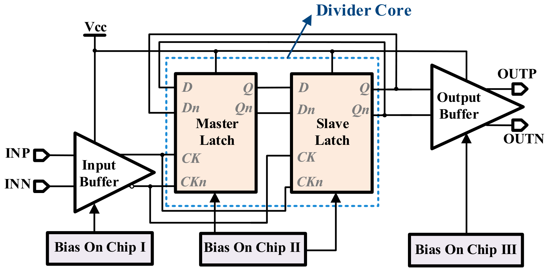
The divider consists of a differential input buffer, a CML master–slave divider core, a differential output buffer, and on-chip bias circuits, as shown in
Figure 1. Independent biasing is used for the major functional blocks, allowing the input matching, core switching speed, and output drive capability to be optimized separately.
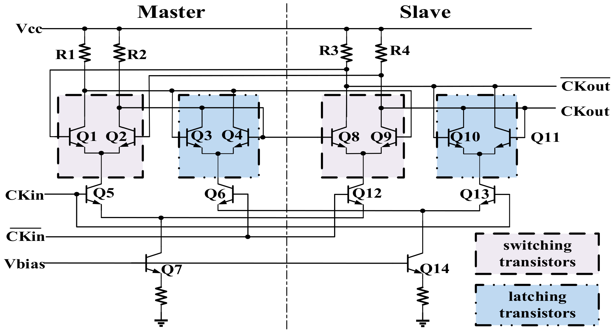
The divider core, shown in
Figure 2, adopts a CML master–slave flip-flop topology to realize static 1:2 frequency division. In this topology, the switching and latching differential pairs dominate the maximum toggling speed and therefore form the main high-frequency bottleneck. Accordingly, 0.5 μm × 5 μm high-
fT DHBTs are used only for the switching pairs Q1/Q2/Q8/Q9 and the latching pairs Q3/Q4/Q10/Q11, while standard 0.7 μm DHBTs are retained for the remaining devices. The 5 μm emitter width was selected through extensive electromagnetic (EM) simulations of all standard 0.5 μm DHBT variants (3 μm, 5 μm, 10 μm, 15 μm emitter widths). A narrower width would limit the maximum switching current, while a wider width would increase parasitic capacitances and degrade high-frequency performance. This selective device allocation reduces parasitic capacitances at the most speed-sensitive nodes without increasing the complexity of the non-critical circuitry. The tail-current network is further optimized to balance switching speed and latch regeneration. The tail transistors Q5/Q12, which control the switching pairs, are designed larger than Q6/Q13, which control the latching pairs, while Q7 and Q14 are sized with a 1:2 ratio. This sizing arrangement is matched to the current density of the 0.5 μm core transistors, ensuring they operate at their peak
fT point across the entire bandwidth. This increases the available switching current for high-speed operation and maintains sufficient regeneration strength over a wide input-frequency range.
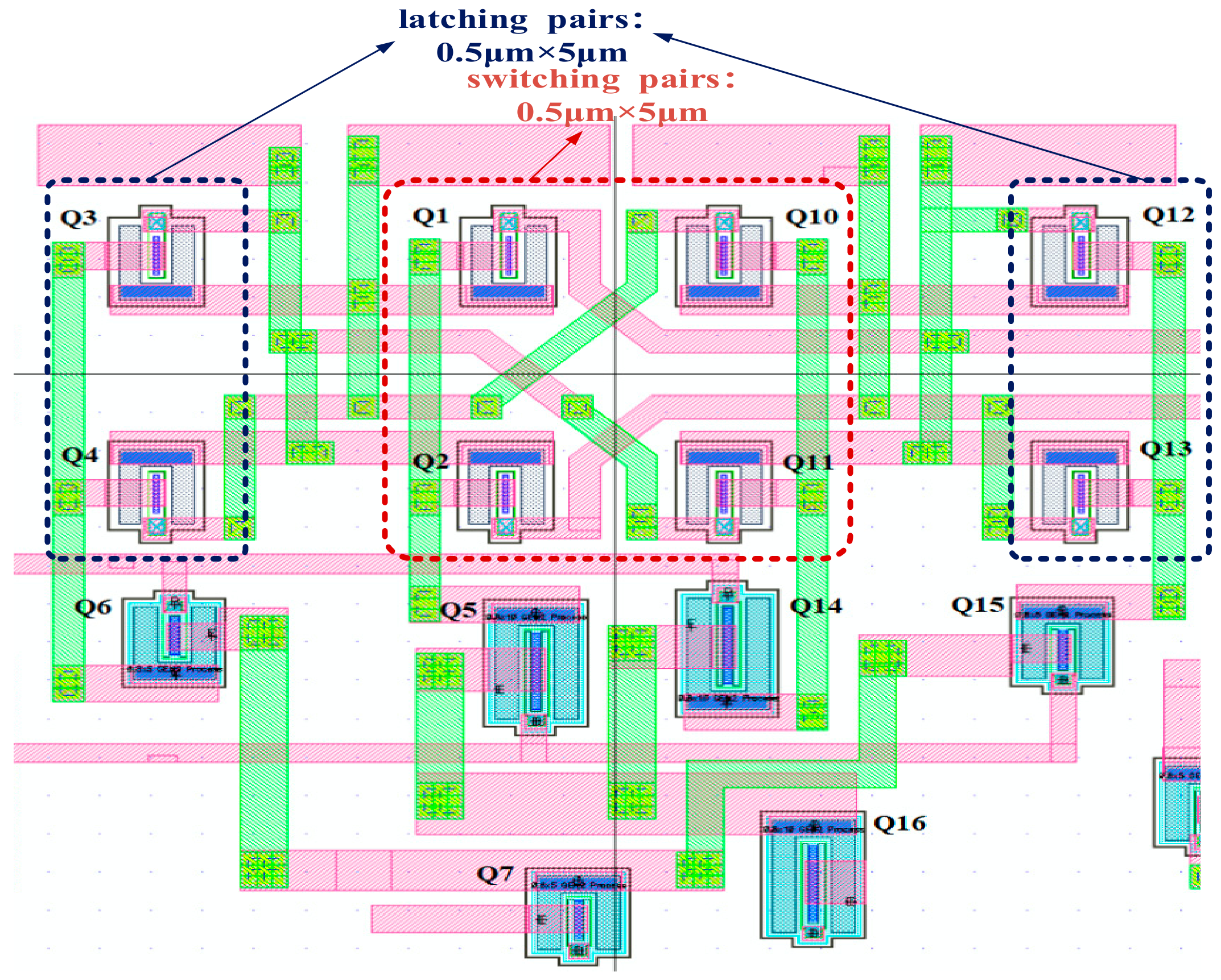
To further suppress parasitic imbalance, a fully centrosymmetric (rotational symmetric) layout is adopted for the divider core, as shown in
Figure 3. The symmetric placement shortens and balances the differential signal paths, reduces parasitic mismatch, suppresses substrate coupling and common-mode noise, and ensures consistent performance of the master and slave latches at millimeter-wave frequencies.
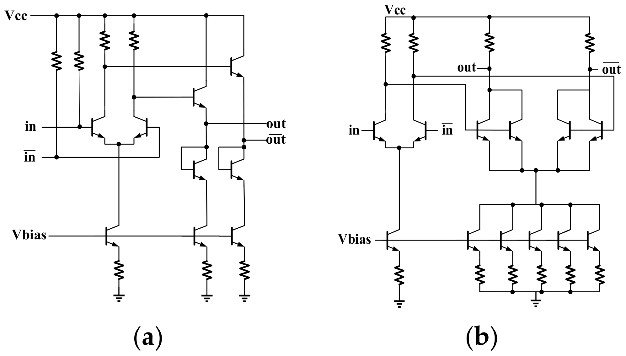
The input buffer, presented in
Figure 4a, uses a cascaded differential amplifier followed by an emitter follower to provide wideband input matching and level shifting. The output buffer, shown in
Figure 4b, adopts parallel differential stages to achieve sufficient drive strength for off-chip measurement and system integration. The on-chip bias provides stable DC operating points for all blocks. The schematic design and simulation of the proposed frequency divider were performed using Keysight ADS 2021 Update 1, Keysight Technologies, Santa Rosa, California, USA.
4. Measured Results
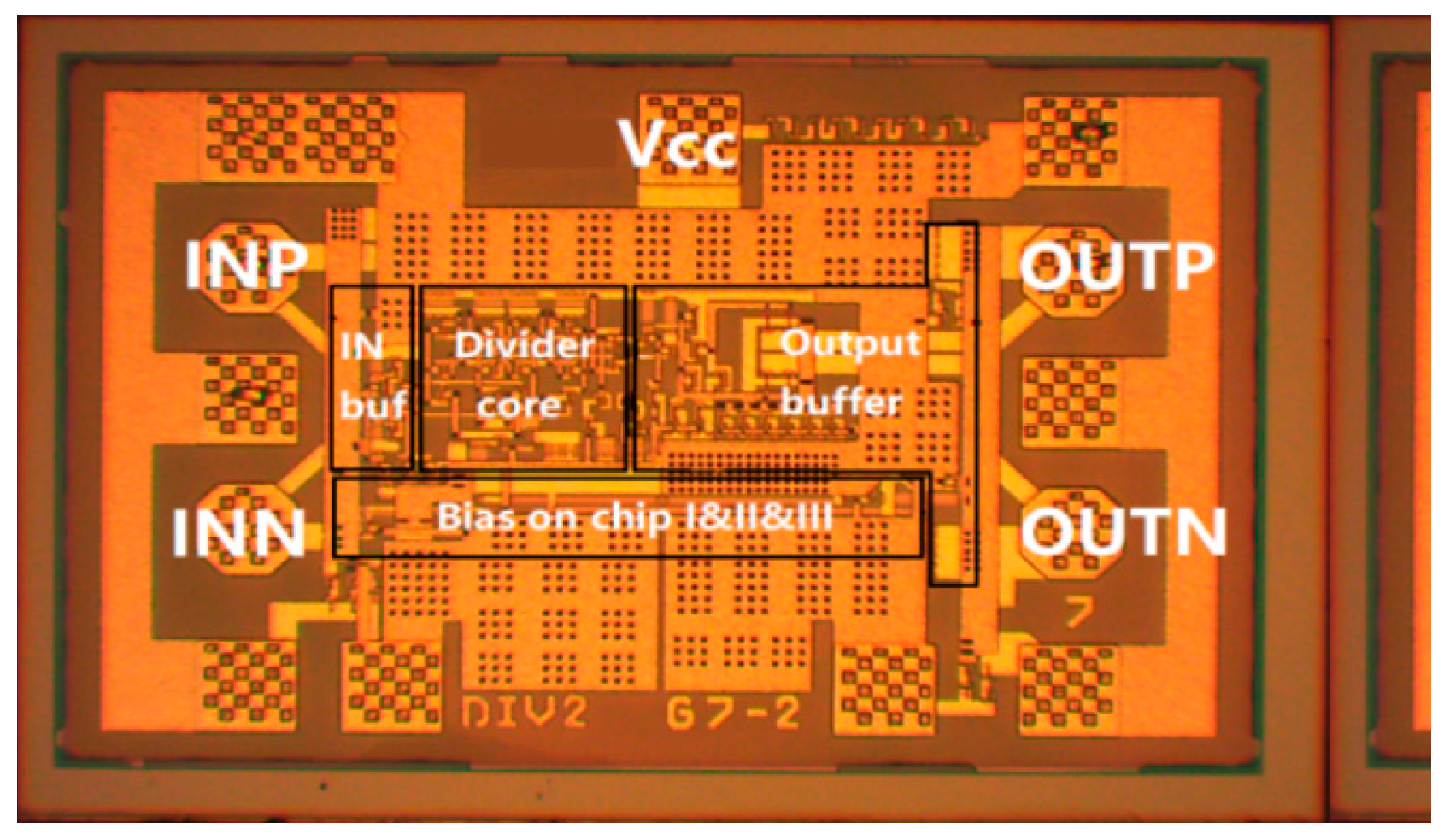
The chip was fabricated in the 0.7 μm InGaAs/InP DHBT technology, with a die size of 0.88 mm × 0.61 mm, as shown in
Figure 5. For measurement, the chip was mounted in a custom-designed metal cavity, and the losses of the measurement setup were calibrated out. The divider operates from a single 3.3 V supply and consumes approximately 350 mW of DC power. The output buffer consumes approximately 120 mW, accounting for 34% of the total power consumption.
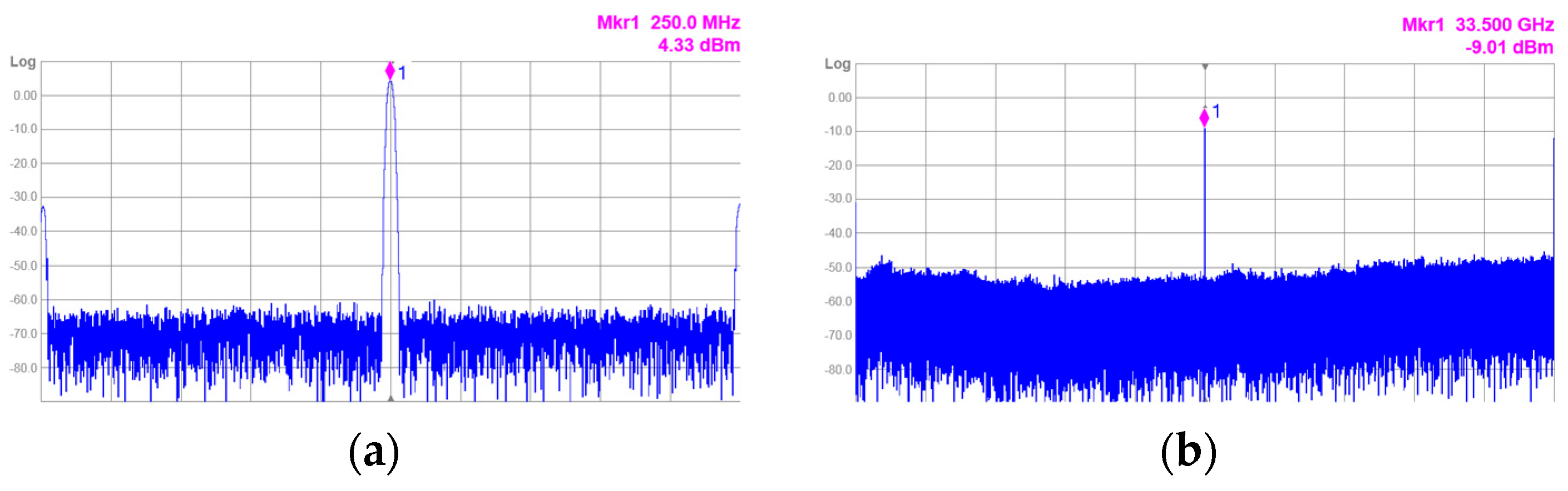
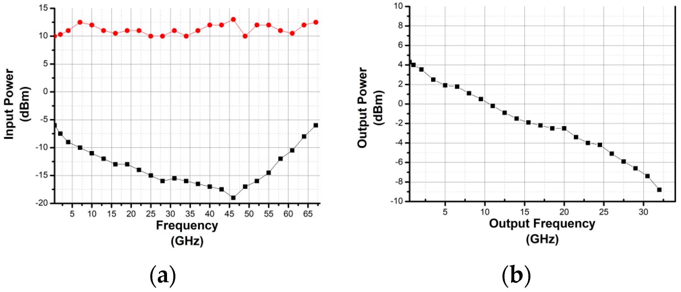
Figure 6 shows the measured output spectra at input frequencies of 0.5 GHz and 67 GHz, verifying stable divide-by-two operation at both the low- and high-frequency ends of the operating band. The measured input power range is plotted in
Figure 7a. Across the full 0.5–67 GHz band, the divider maintains stable frequency division for input power levels from −5 to +10 dBm, indicating a wide input drive tolerance for broadband operation. The measured single-ended output power versus frequency is shown in
Figure 7b. The output power varies from −9 to +4.5 dBm across the operating band and remains above −10 dBm over the full frequency range.
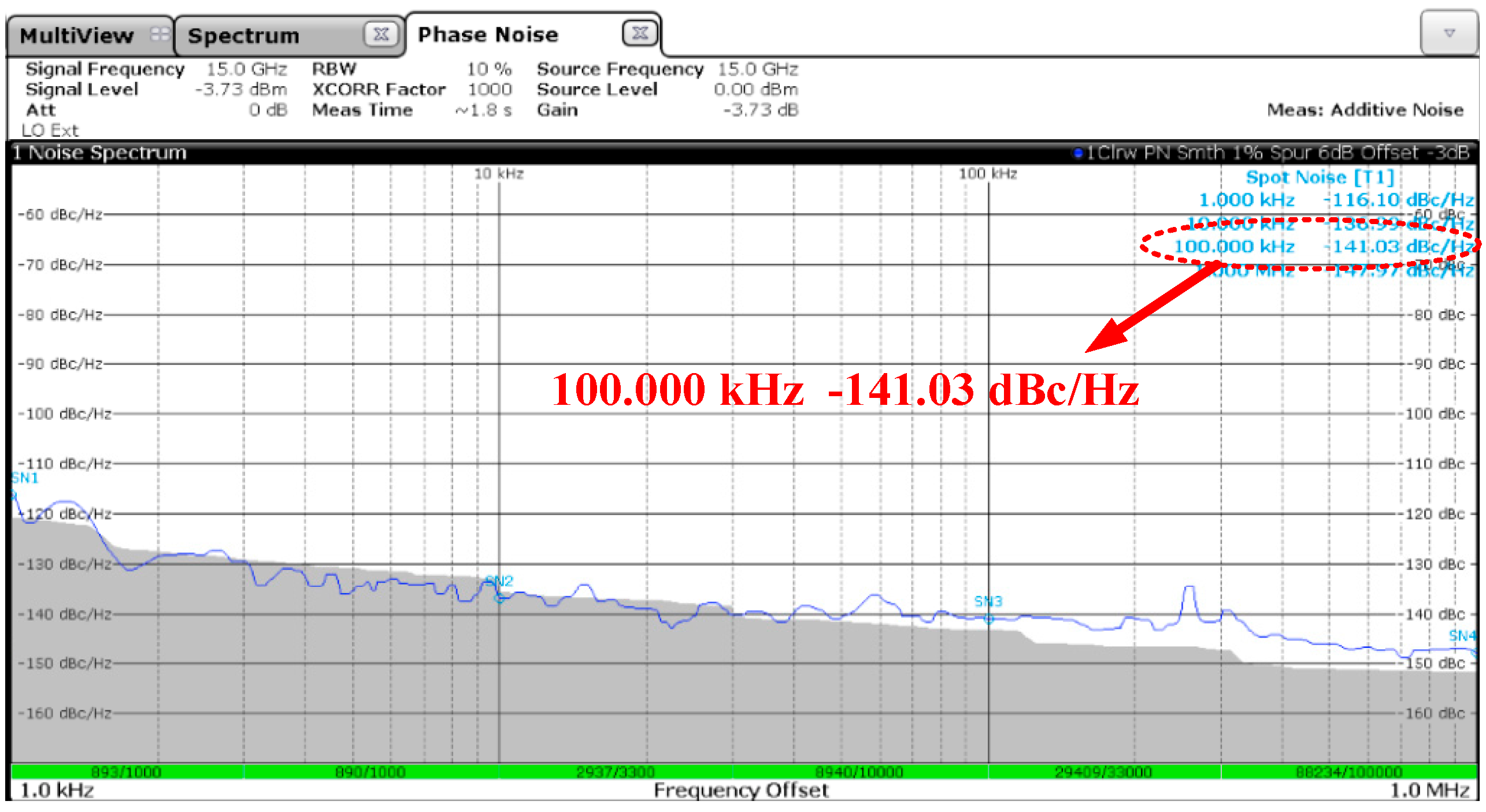
Figure 8 presents the measured single-sideband phase noise with a 30 GHz input. At a 100 kHz offset, the divider achieves an SSB phase noise of −141.03 dBc/Hz. This result indicates that the proposed mixed-device core maintains low-noise operation while extending the high-frequency division range. The input RF signal was provided by an E8257D microwave signal source (Keysight Technologies, Santa Rosa, CA, USA). The output frequency and phase noise characteristics were measured using an FSWP phase noise and and spectrum analyzer (Rohde & Schwarz, Munich, Germany).
Table 1 compares the performance of this work with previously reported state-of-the-art static frequency dividers. A widely used figure of merit (FoM) for static frequency dividers is defined as FoM = BW∙
fmax/
PDC [
14]. It should be noted that alternative FoM definitions exist in the literature, such as
fmax/
PDC and SOF/
PDC, which focus primarily on high-frequency performance. For wideband frequency dividers targeting broadband communication systems, the FoM incorporating both bandwidth and maximum frequency provides a more comprehensive characterization of overall performance.
5. Discussion
The measured results confirm that selective core transistor scaling based on a standard CML architecture can significantly extend operating bandwidth and increase maximum frequency, achieving a 56% improvement in upper frequency limit compared with our previous work without transistor scaling [
1]. This approach also effectively reduces circuit complexity: compared with the
fT-doubler topology in [
10], which requires 16 transistors per latch, the proposed CML core only uses seven transistors per latch, significantly simplifying design and layout.
Notably, the proposed design achieves a wider full-band input power range than most reported works, which is a critical advantage for practical system integration. The excellent phase noise performance further enhances its suitability for high-quality local oscillator generation in broadband communication systems.
Although the output power variation is relatively large (−9–+4.5 dBm), it remains well within the input power range of this work. For applications requiring more uniform output power, a two-stage cascaded divider configuration can be employed to flatten the output power response across the full bandwidth.
6. Conclusions
A 0.5–67 GHz CML static 1:2 frequency divider is demonstrated in a commercial 0.7 μm InGaAs/InP DHBT technology. By selectively introducing 0.5 μm high-fT DHBTs into the speed-critical switching and latching pairs, the mixed-device design improves the high-frequency capability of the divider core without full process migration or major topology modification. The fabricated divider achieves a continuous operating range of 0.5–67 GHz, a full-band input power range of −5 to +10 dBm, single-ended output power above −10 dBm, and an SSB phase noise of −141.03 dBc/Hz at 100 kHz offset with a 30 GHz input. The results verify that selective core transistor scaling provides a practical route for wideband static dividers on mature InP DHBT platforms.
Author Contributions
Conceptualization, M.Z. and Q.M.; methodology, M.Z.; validation, M.Z., Y.Z. (Youtao Zhang), L.C. and Y.Z. (Yi Zhang); formal analysis, M.Z. and Y.Z. (Youtao Zhang); investigation, M.Z.; resources, Q.M.; data curation, M.Z.; writing—original draft preparation, M.Z.; writing—review and editing, Y.Z. (Yi Zhang); visualization, M.Z.; supervision, Y.Z. (Youtao Zhang); project administration, Q.M.; funding acquisition, Q.M. All authors have read and agreed to the published version of the manuscript.
Funding
This work was supported in part by the National Natural Science Foundation of China under Grant 61804081, in part by the Open Foundation of Science and Technology on Monolithic Integrated Circuits and Modules Laboratory under Grant 614280304012101 and in part by the Jiangsu Provincial Postgraduate Research and Practice Innovation Program under Grant KYCX25_1143.
Institutional Review Board Statement
Not applicable.
Informed Consent Statement
Not applicable.
Data Availability Statement
The original contributions presented in this study are included in the article. Further inquiries can be directed to the corresponding author.
Acknowledgments
The authors would like to thank Wei Cheng for his valuable technical support on the InP DHBT process. The authors declare that no generative AI tools were used in the preparation of this manuscript.
Conflicts of Interest
Authors Min Zhang and Youtao Zhang was employed by the Nanjing GuoBo Electronics Co., Ltd. The remaining authors declare that the research was conducted in the absence of any commercial or financial relationships that could be construed as a potential conflict of interest.
References
- Zhang, M.; Li, X.; Zhang, Y.; Cheng, W. 0.5~43 GHz 1:2 Static Frequency Divider MMIC in InP HBT Technology. In Proceedings of the 2019 International Conference on IC Design and Technology, Suzhou, China, 17–19 June 2019; pp. 288–290. [Google Scholar] [CrossRef]
- Chien, H.-Y.; Chen, C.; Chen, R.; Woo, J.; Pamarti, S.; Chang, M.-C.F. A Low Power 185 GHz Static CML Frequency Divider in SiGe HBTs Using Band-switching Technique in 45nm PDSOI BiCMOS. In Proceedings of the 2024 IEEE/MTT-S International Microwave Symposium, Washington, DC, USA, 16–21 June 2024; pp. 174–177. [Google Scholar] [CrossRef]
- Xiao, Y. A Wideband Static CMOS Divide-by-2 Frequency Divider for Low-Power RF Applications. In Proceedings of the 2025 7th International Conference on Electronics and Communication, Network and Computer Technology, Guangzhou, China, 18–20 July 2025; pp. 18–20. [Google Scholar] [CrossRef]
- Vogelsang, F.; Bredendiek, C.; Schöpfel, J.; Rücker, H.; Pohl, N. A Static Frequency Divider up to 163 GHz in SiGe-BiCMOS Technology. In Proceedings of the 2022 IEEE BiCMOS and Compound Semiconductor Integrated Circuits and Technology Symposium, Phoenix, AZ, USA, 16–19 October 2022; pp. 49–52. [Google Scholar] [CrossRef]
- Griffith, Z.; Dahlström, M.; Rodwell, M.J.W.; Urteaga, M.; Pierson, R.; Rowell, P. Ultra high frequency static dividers > 150 GHz in a narrow mesa InGaAs/InP DHBT technology. In Proceedings of the 2004 Bipolar/BiCMOS Circuits and Technology Meeting, Montreal, QC, Canada, 12–14 September 2004; pp. 176–179. [Google Scholar] [CrossRef]
- Patnaik, A.; Yoon, D. A 24–64 GHz Wideband Static CML Frequency Divider in a 90-nm CMOS Technology. IEEE Microw. Wirel. Technol. Lett. 2025, 35, 71–74. [Google Scholar] [CrossRef]
- Zhang, Y.; Li, X.; Zhang, M.; Cheng, W.; Chen, X. A 83 GHz InP DHBT static frequency divider. J. Semicond. 2014, 35, 045004. [Google Scholar] [CrossRef]
- Ali, U.; Bober, M.; Thiede, A.; Awny, A.; Fischer, G. High speed static frequency divider design with 111.6 GHz self-oscillation frequency (SOF) in 0.13 µm SiGe BiCMOS technology. In Proceedings of the 2015 German Microwave Conference, Nuremberg, Germany, 16–18 March 2015; pp. 241–243. [Google Scholar] [CrossRef]
- Dyskin, A.; Kallfass, I. Analytical Approach for SiGe HBT Static Frequency Divider Design for Millimeter-Wave Frequency Operation. IEEE Trans. Microw. Theory Tech. 2018, 66, 1411–1417. [Google Scholar] [CrossRef]
- Zhen, W.; Zhang, Y.; Wang, Z.; Liu, Y.; Zhao, Y. RF performance improvement of InP frequency divider by using enhanced ft-doubler technique. IEEE Microw. Wirel. Compon. Lett. 2022, 32, 1063–1066. [Google Scholar] [CrossRef]
- Griffith, Z.; Urteaga, M.; Pierson, R.; Rowell, P.; Rodwell, M.J.W.; Brar, B. A 204.8 GHz static divide-by-8 frequency divider in 250 nm InP HBT technology. In Proceedings of the 2010 IEEE Compound Semiconductor Integrated Circuit Symposium, Monterey, CA, USA, 3–6 October 2010; pp. 1–4. [Google Scholar] [CrossRef]
- Chien, H.-Y.; Chen, C.; Woo, J.; Pamarti, S.; Yang, C.-K.K.; Chang, M.-C.F. A Low Power 100 GHz Static CML Frequency Divider in 0.18 μm SiGe BiCMOS Technology. In Proceedings of the 2023 IEEE 23rd Topical Meeting on Silicon Monolithic Integrated Circuits in RF Systems, Las Vegas, NV, USA, 22–25 January 2023; pp. 1–4. [Google Scholar] [CrossRef]
- Griffith, Z.; Parthasarathy, N.; Rodwell, M.J.W.; Urteaga, M.; Shinohara, K.; Rowell, P.; Pierson, R.; Brar, B. An Ultra Low-Power (≤13.6 mW/latch) Static Frequency Divider in an InP/InGaAs DHBT Technology. In Proceedings of the 2006 IEEE MTT-S International Microwave Symposium, San Francisco, CA, USA, 11–16 June 2006; pp. 1579–1582. [Google Scholar] [CrossRef]
- Ghilioni, A.; Decanis, U.; Mazzanti, A.; Svelto, F. A 4.8 mW inductorless CMOS frequency divider-by-4 with more than 60% fractional bandwidth up to 70 GHz. In Proceedings of the 2012 IEEE Custom Integrated Circuits Conference, San Jose, CA, USA, 9–12 September 2012; pp. 1–4. [Google Scholar] [CrossRef]
| Disclaimer/Publisher’s Note: The statements, opinions and data contained in all publications are solely those of the individual author(s) and contributor(s) and not of MDPI and/or the editor(s). MDPI and/or the editor(s) disclaim responsibility for any injury to people or property resulting from any ideas, methods, instructions or products referred to in the content. |