2.1. Low-Pass SSPP Unit Design
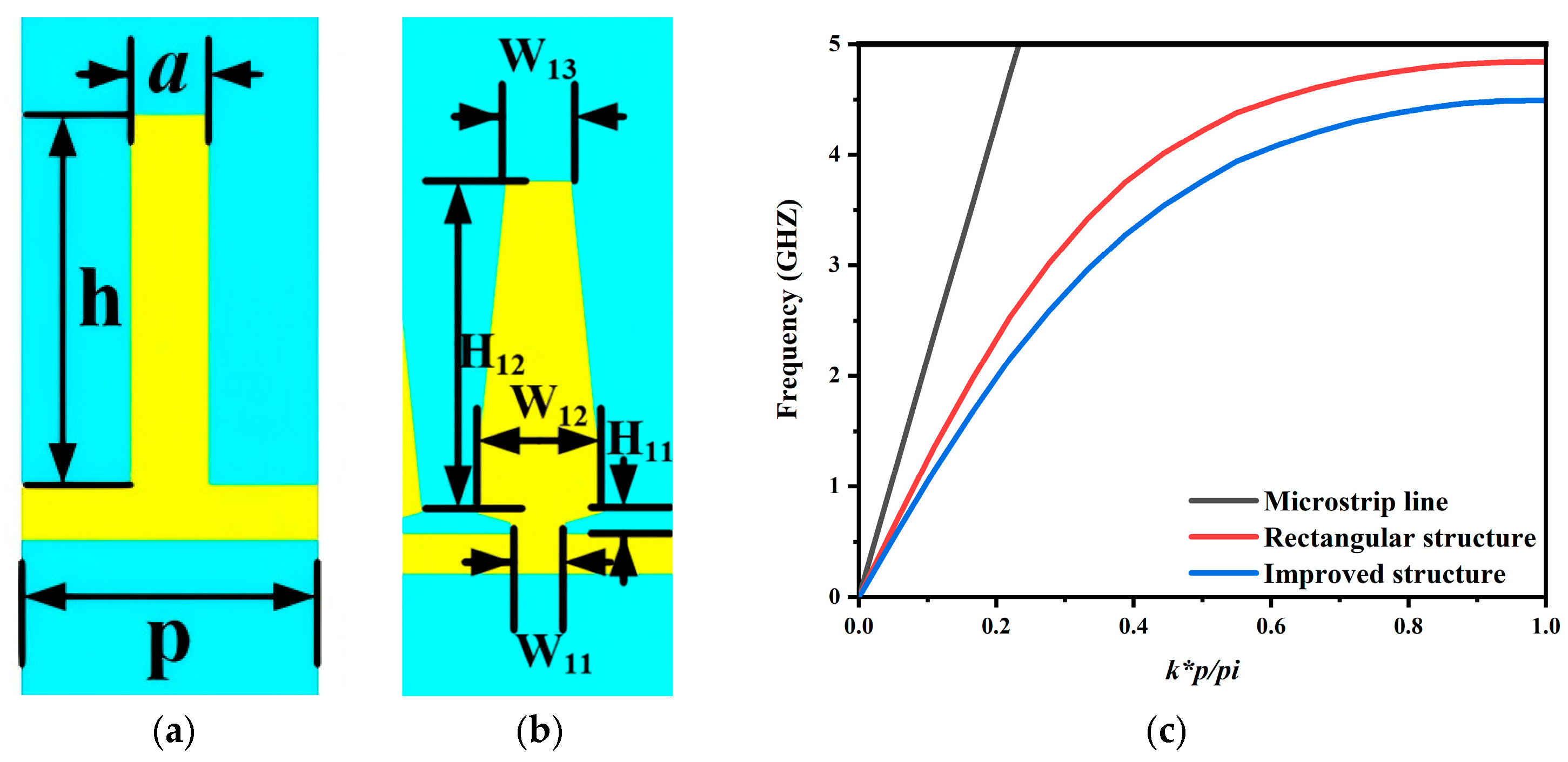
Figure 1a shows a conventional rectangular SSPP unit cell. Its dispersion follows the periodic metal gap structure theory reported by Harrington [
21], as expressed in Equation (1) [
22]. In this topology the groove depth h mainly determines the cutoff frequency. Only h and the groove width a provide effective tuning. This limits design flexibility and restricts miniaturization. To address these issues an improved SSPP unit cell is introduced in
Figure 1b. It incorporates several additional adjustable geometrical parameters. The dispersion of the proposed unit cell is extracted in CST Microwave Studio using the eigenmode procedure in [
23]. The dispersion curve of the microstrip line is plotted as a reference. As shown in
Figure 1c, as the frequency increases, the dispersion curves of both unit cell structures gradually deviate from that of the microstrip line and approach their respective asymptotic frequencies at 4.5 GHz and 5 GHz. This behavior clearly indicates the enhancement of field confinement. For the same unit cell height, the improved structure exhibits a lower asymptotic frequency. This feature implies stronger electromagnetic field confinement and demonstrates a greater capability for miniaturization. The dispersion curves in
Figure 1c are obtained in CST Microwave Studio. The dispersion characteristics of the SSPP unit cell are evaluated by embedding the proposed cell in an air box. Periodic boundary conditions are applied along the y-direction, while PEC boundaries are imposed on the x- and z-direction faces. Eigen frequencies are then computed by sweeping the phase shift between the two periodic boundaries from 0° to 180°. In this way, the dispersion relation of the fundamental mode is extracted, where k represents the propagation constant along the y-axis.
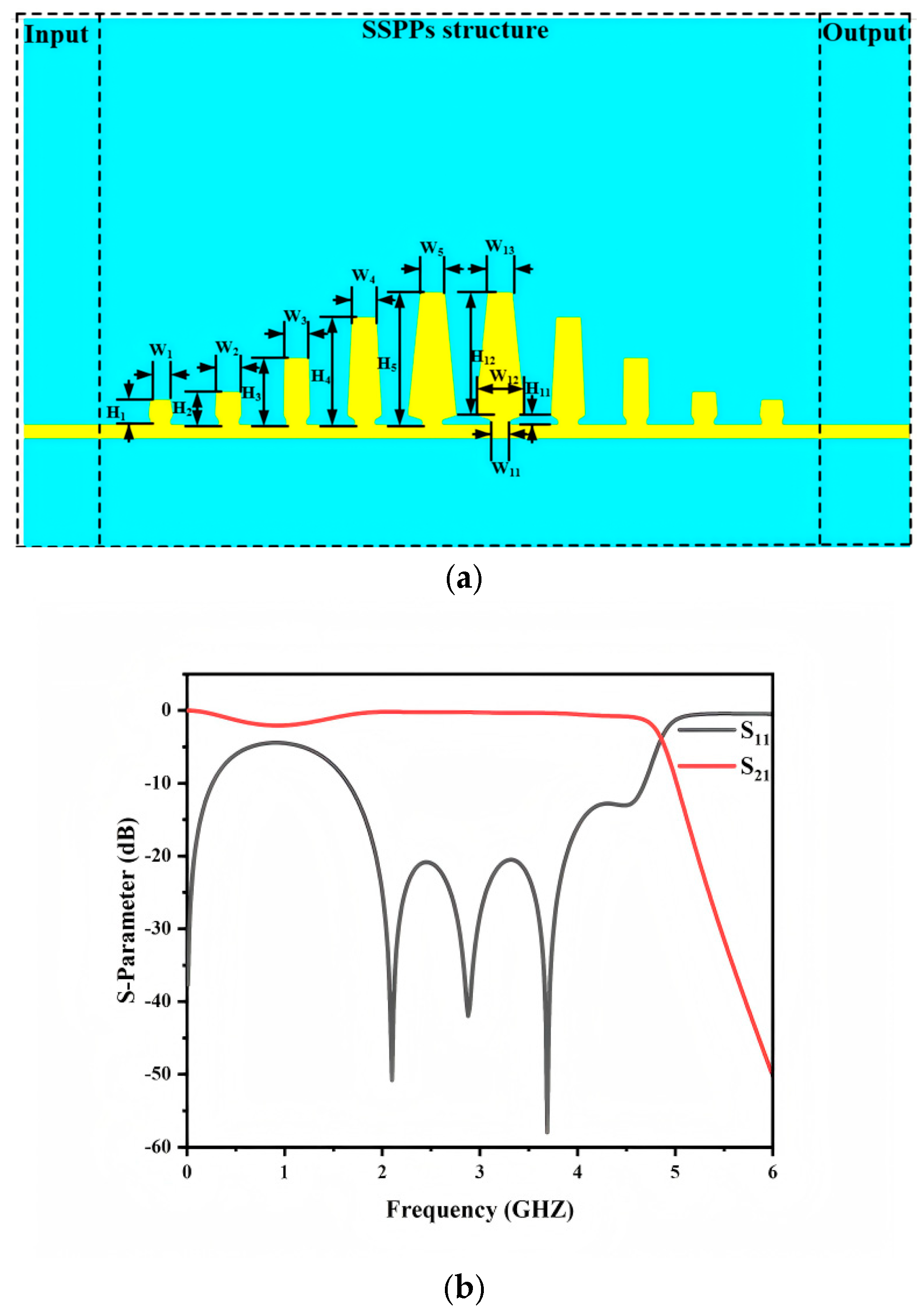
Compared with conventional microstrip lines, SSPP transmission lines inherently exhibit a low-pass dispersion. This property provides a natural upper cutoff frequency, which is advantageous for bandpass filter design. By cascading the proposed unit cells with different heights, a low-pass filter is implemented, as shown in
Figure 2a. The simulated S-parameters are presented in
Figure 2b. The return loss within the passband is generally better than −10 dB, confirming that the improved SSPP unit cell supports a high performance low-pass response. A degraded return loss is observed around 1 GHz. This behavior is mainly attributed to momentum mismatch between the input microstrip port and the SSPP section. In this work, the low-frequency mismatch is acceptable because the subsequent bandpass design intentionally introduces low-frequency suppression. Therefore, the degraded matching around 1 GHz has a limited impact on the overall filter performance.
2.2. Design of a Bandpass Filter Based on SSPP Structure
Bandpass filter design requires the establishment of both upper and lower cutoff frequencies. As discussed in
Section 2.1, cascading the improved SSPP unit cells with different heights and widths produces a low-pass response. Its cutoff frequency naturally defines the upper band edge and provides effective suppression for undesired signals above the passband. To realize the lower cutoff frequency, a dedicated attenuation mechanism must be introduced at low frequencies. Commonly used methods include using SIW, microstrip-slot-line structures, or short-circuited stubs. The first two approaches increase structural complexity and fabrication difficulty, which can degrade the measured performance of the fabricated prototype. Therefore short-circuited stubs are incorporated into the SSPP unit cells to form resonant units. The resulting resonance introduces low-frequency suppression and establishes the lower cutoff required for the proposed bandpass filter.
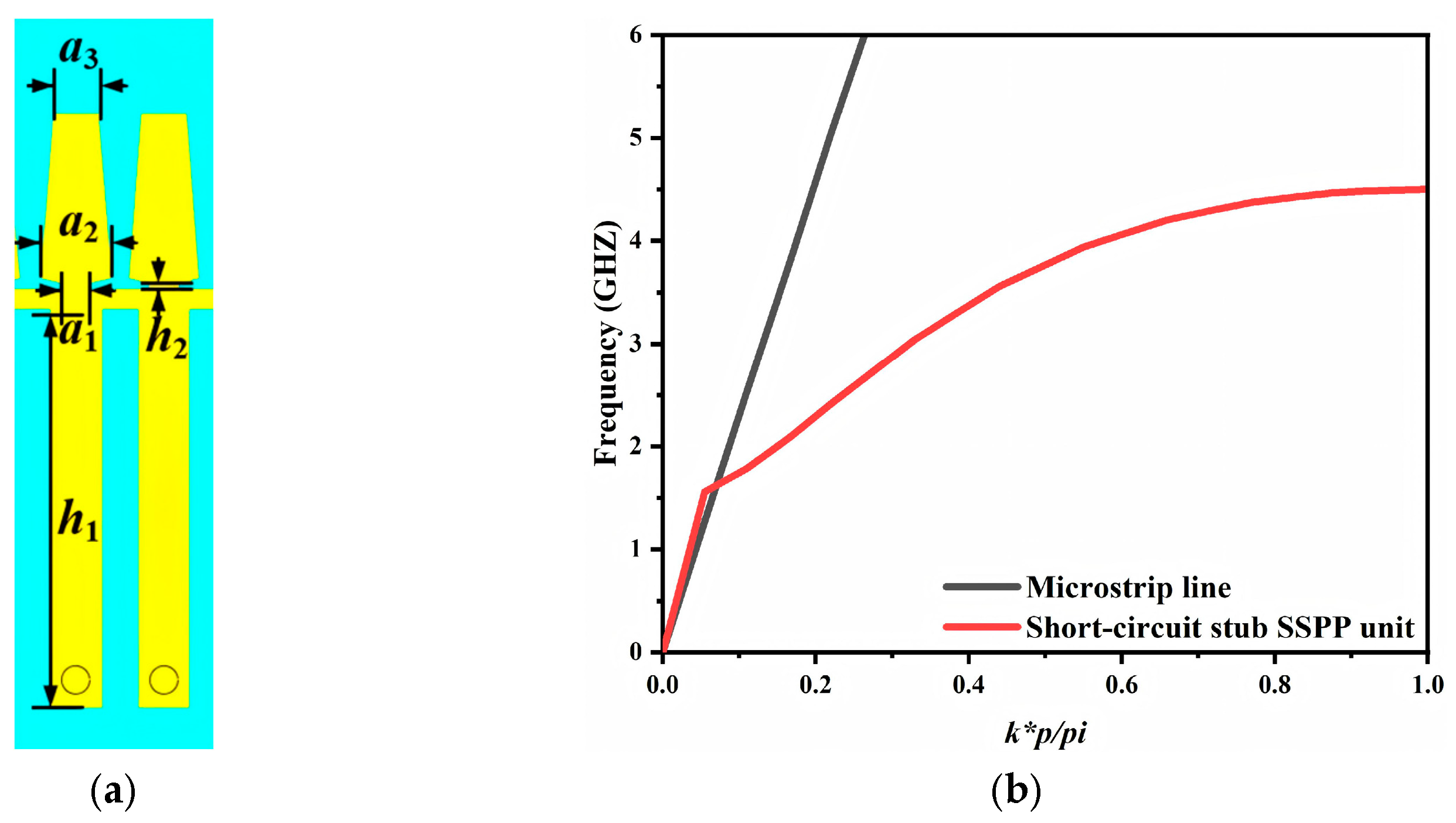
The designed SSPP resonant unit is depicted in
Figure 3a. The proposed SSPP cell and the short-circuited stub are symmetrically loaded on the two sides of the main transmission line. The stub is connected to the bottom ground plane through a grounding via, thereby forming the required current return path. The number of SSPP resonant units is also a critical design parameter. Increasing the number of units generally flattens the passband response and improves out of band rejection. However, it also enlarges the circuit footprint and limits the degree of miniaturization. Considering these tradeoffs, two SSPP resonant units are employed in this work. This choice satisfies the required in-band transmission while maintaining a compact overall size.
The dispersion characteristics of a single unit cell are shown in
Figure 3b. The dispersion curve of a microstrip line is also plotted for comparison. At low frequencies, the dispersion of the short-circuited SSPP unit cell closely follows the light line and gradually departs from it as frequency increases. It eventually approaches a constant value, referred to as the asymptotic frequency. This asymptotic frequency determines the upper cutoff of the resulting bandpass filter. In addition, an intersection between the two dispersion curves appears in the low-frequency region. This intersection is associated with the lower cutoff frequency. As indicated in
Figure 3b, the asymptotic frequency is approximately 4.6 GHz and the intersection frequency is approximately 1.6 GHz. Therefore, based on this short-circuited SSPP unit cell the upper cutoff frequency is expected to be around 4.6 GHz, whereas the lower cutoff frequency is around 1.6 GHz.
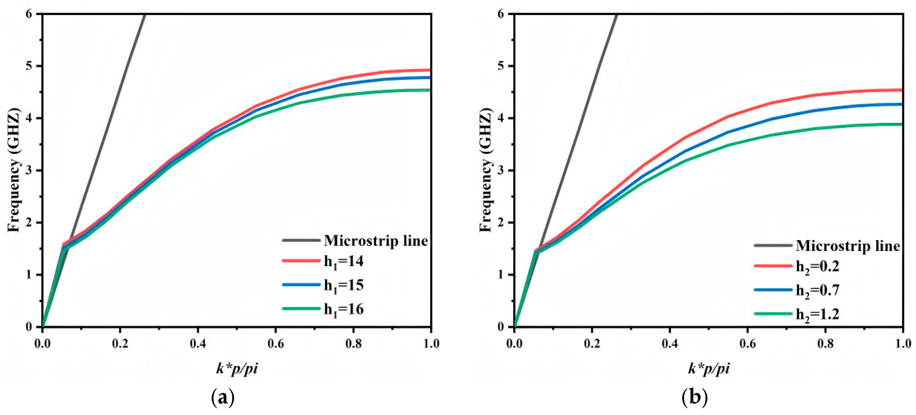
Furthermore, the proposed short-circuited stub unit cell enables dispersion tailoring through geometric tuning. As shown in
Figure 4a,b, varying h
1 and h
2 shifts the asymptotic frequency, whereas the intersection point in the low-frequency region remains nearly unchanged. Consequently, the upper cutoff frequency can be flexibly adjusted while the lower cutoff frequency is essentially preserved. As h
1 and h
2 increase, the asymptotic frequency decreases and the upper cutoff frequency reduces accordingly. This behavior provides a direct and convenient approach for passband bandwidth adjustment during the design stage.
Based on the above design, the upper and lower cutoff frequencies can be established, thereby yielding a bandpass response. However, the dispersion relation indicates a pronounced momentum mismatch between the microstrip line and the short-circuited stub SSPP unit. If the SSPP resonator is directly connected to the microstrip line, strong passband ripples will occur and additional insertion loss may be introduced, thereby degrading the filter performance. Therefore, a dedicated transition section is required between the microstrip feed and the SSPP resonator to enable smooth mode conversion from the microstrip mode to the SSPP mode while preserving the bandpass characteristics. The low-pass filter introduced in
Section 2.1 can be employed as an effective transition unit. It provides momentum matching and a gradual impedance transformation.
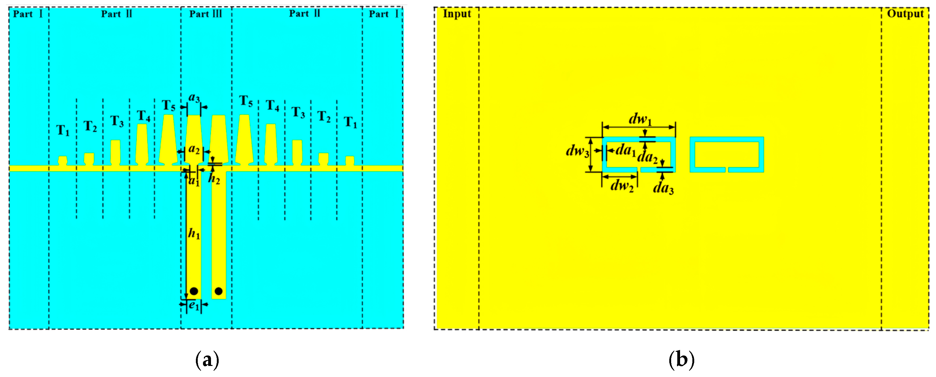
Based on the proposed configuration, the overall bandpass filter layout is illustrated in
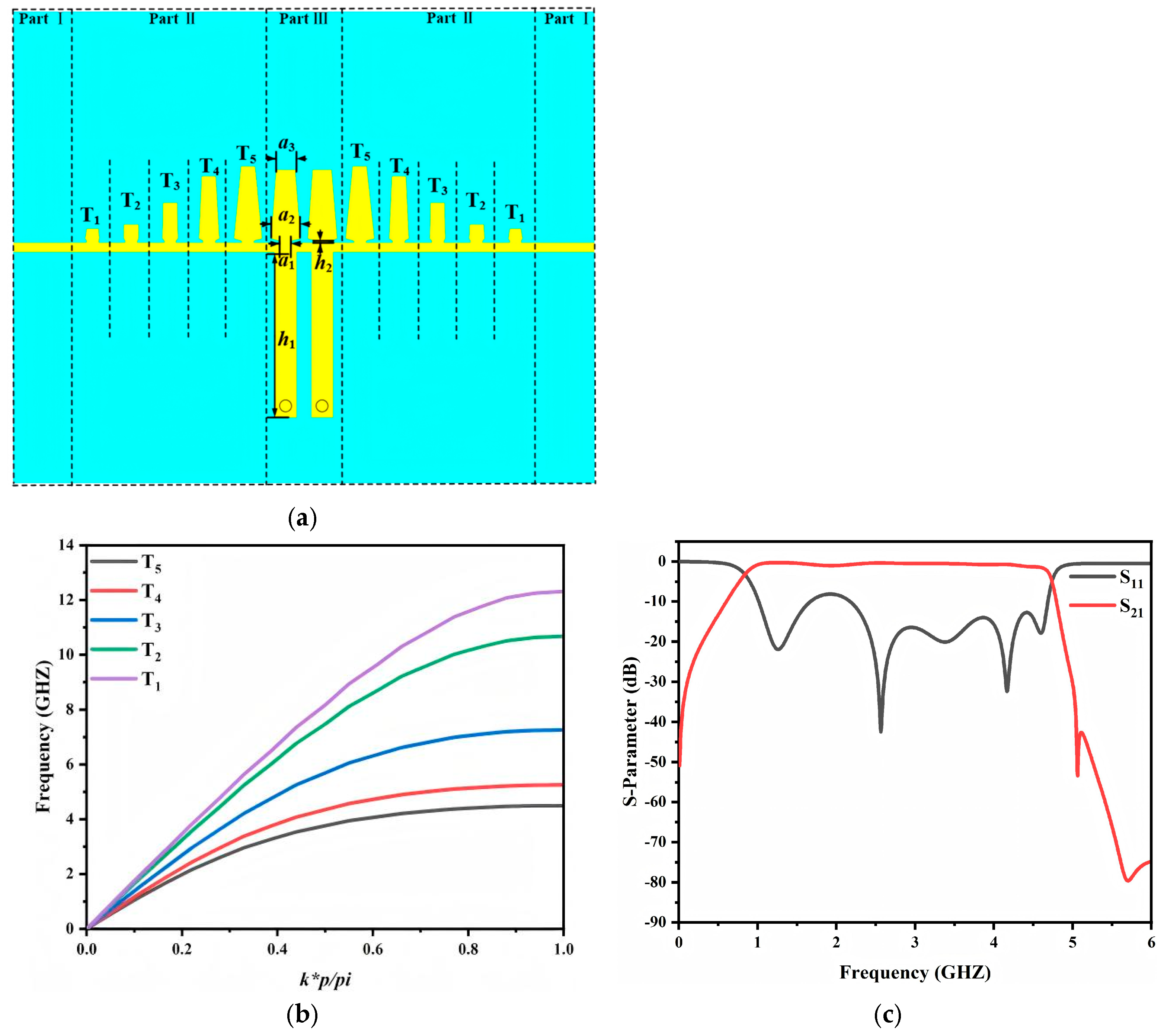
Figure 5a. The circuit consists of three regions. Region I is the feed section, implemented by a 50 Ω microstrip line with a width of 0.72 mm. Region II is the transition section, which comprises five cascaded units with gradually varied heights and widths. This section is derived from the low-pass SSPP structure in
Section 2.1 and provides momentum matching and impedance transformation between the microstrip line and the SSPP resonant transmission line. Region III is the main transmission section, formed by two proposed SSPP resonant units.
Furthermore, the dispersion curves of the transition section are shown in
Figure 5b. The asymptotic frequency evolves monotonically from T
1 to T
5. It shifts from a value close to that of the microstrip line to a value approaching that of the SSPP resonant unit. This continuous evolution indicates that the proposed transition section provides effective momentum matching between the microstrip mode and the SSPP mode, enabling smooth energy transfer across the transition region and preserving stable in-band transmission. The simulated S-parameters of the overall bandpass filter are plotted in
Figure 5c. A clear passband is obtained from 1.0 to 4.6 GHz. The insertion loss remains better than −3 dB over the passband. The filter also exhibits satisfactory out-of-band rejection. This response provides a suitable baseline for the subsequent notch integrated bandpass filter design.
A clear passband is observed from 1.0 to 4.6 GHz, with the insertion loss remaining better than −3 dB throughout the passband. The filter also demonstrates satisfactory out-of-band rejection, providing a suitable baseline for the subsequent notch-integrated bandpass filter design.
2.3. Design of a Notch Bandpass Filter Based on SSPPs
Defected ground structures (DGSs) are formed by etching periodic or aperiodic patterns into the ground metallization of a planar transmission line. This perturbation distorts the surface current distribution and modifies the local electromagnetic boundary conditions. As a result, the effective inductance and capacitance of the transmission line are altered. For microstrip implementations, the introduction of a DGS typically increases both the equivalent inductance and the equivalent capacitance.
The earliest defected ground structure is the dumbbell-shaped DGS [
24]. It consists of two rectangular defect regions that are coupled through a narrow gap and connected by a thin slot etched in the ground plane. DGSs are attractive because they can provide bandstop behavior without requiring a large periodic array. A small number of DGS cells are often sufficient to obtain pronounced rejection while keeping the circuit footprint small. In addition, a single DGS element features a simple geometry that is easy to fabricate, and its equivalent circuit model can be conveniently established and extracted. Moreover, the slow wave effect can be achieved with only one or several cells, which simplifies practical implementation. Motivated by these advantages, this section introduces a DGS into the proposed bandpass filter to generate an in-band notch. The resulting notch enables targeted suppression at a specified interference frequency.
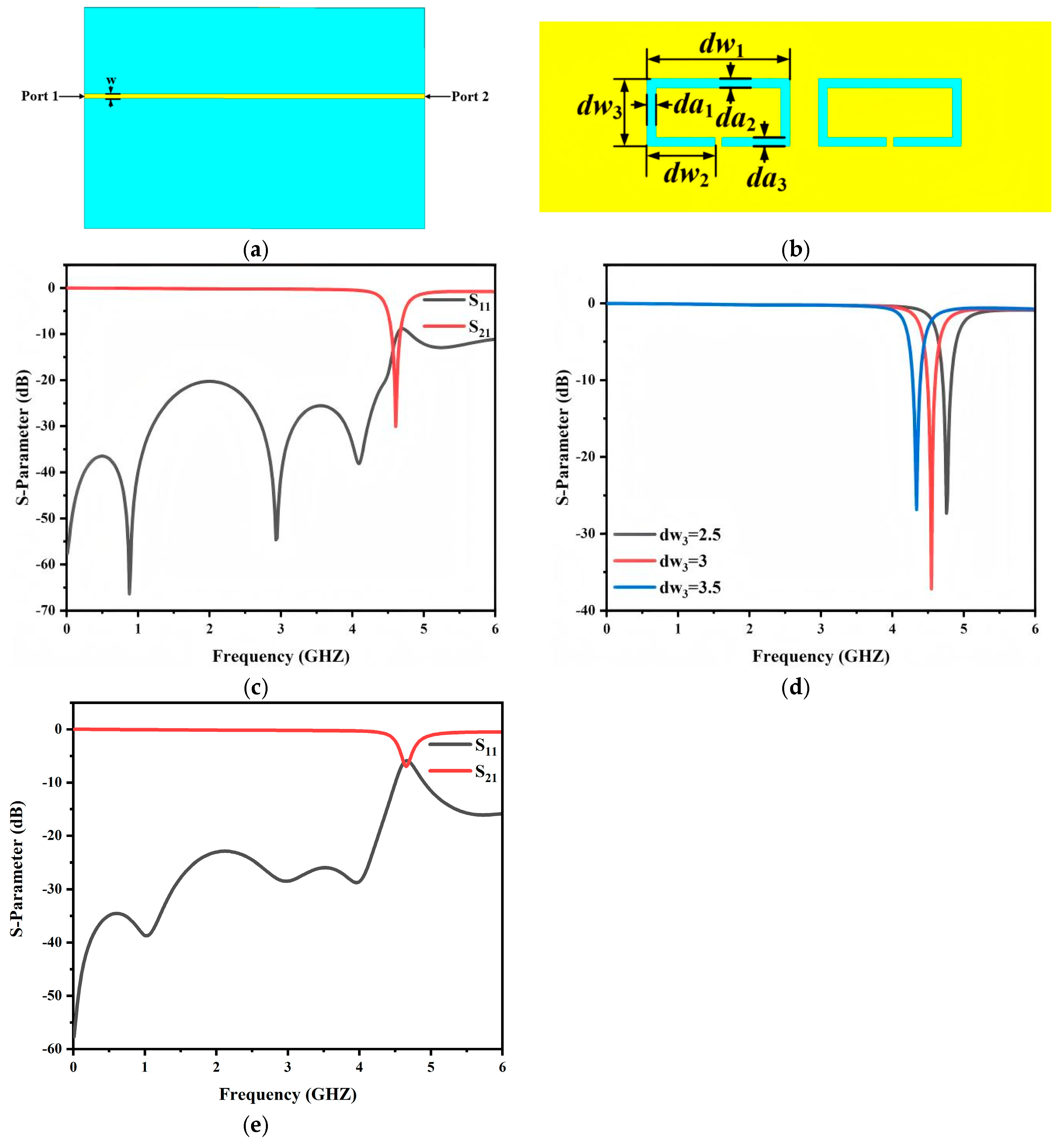
Despite the aforementioned advantages, the conventional dumbbell-shaped DGS still occupies a relatively large etched area on the ground plane due to its two-slot configuration. This becomes a limiting factor when further miniaturization and high integration are required in the proposed filter. To alleviate this constraint, an open-slot annular DGS is adopted, as shown in
Figure 6b. Compared with the traditional dumbbell topology, the proposed structure exhibits a more compact layout and requires less ground plane area while maintaining the desired bandstop characteristic. In addition, the slot length and slot width provide effective tuning parameters for accurately controlling the notch frequency, thereby enabling targeted suppression near the specified interference band within a constrained footprint.
To clearly demonstrate the electromagnetic characteristics of the proposed annular DGS, a 50 Ω microstrip feed line with a width of 0.72 mm is introduced at the input side of the simulation model, and wave ports are assigned at both ends of the microstrip line, as illustrated in
Figure 6a. The annular defect is etched on the backside ground metallization, as depicted in
Figure 6b. Consequently, the proposed DGS improves ground plane utilization and supports further miniaturization and integration while preserving the required filtering performance.
Figure 6c plots the simulated S
11 and S
21 of the proposed DGS. A pronounced notch is clearly observed in the target band. It exhibits deep attenuation, which confirms strong rejection capability. This response effectively suppresses the undesired spectral components at the specified frequency.
To investigate the influence of the slot DGS parameters on the notch behavior the transmission responses under different dw
3 values are presented. As shown in
Figure 6d increasing dw
3 shifts the notch frequency toward the lower band. This trend can be interpreted using an equivalent circuit model. A larger dw
3 effectively extends the slot line length and increases the effective slot area. The corresponding series equivalent inductance therefore increases. Since the resonant frequency decreases with increasing inductance, the notch frequency moves to a lower value accordingly [
25]. Hence the notch frequency can be controlled within a certain range during the design stage by adjusting dw
3. Moreover, an appropriate choice of dw
3 enables accurate notch placement while preserving a compact layout and simple implementation, thereby enhancing the applicability and tuning flexibility of the proposed DGS in microwave circuits.
Furthermore, the number of annular slots directly affects the notch characteristics. Each annular slot introduces a localized resonance that contributes to the suppression within the passband. When only one slot is used, as shown in
Figure 6e, the notch suppression depth is limited to approximately −7 dB. Introducing a second slot, as in
Figure 6c, provides an additional resonance, enhancing the suppression depth to −25 dB. From a theoretical perspective, the number of slots is also related to the number of SSPP resonant cells in the bandpass filter. Since the designed filter employs two SSPP resonators, using two annular slots ensures mode matching between the resonators and the notches, achieving efficient suppression at the target frequency. Using more than two slots may lead to undesired coupling between resonances, complicating the notch response and potentially degrading the overall passband performance. Therefore, considering both the notch suppression depth and the resonance alignment with the SSPP cells, two annular slots are adopted in this design.
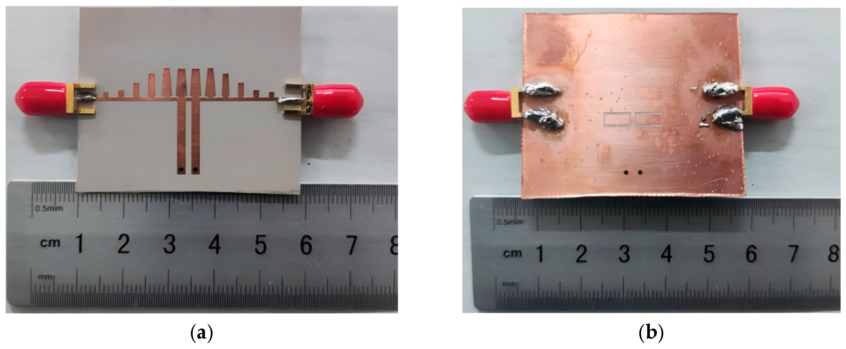
By etching the proposed DGS onto the ground plane of the bandpass filter described in the previous section, a notch response is incorporated into the original bandpass characteristic. The final notch bandpass filter is illustrated in
Figure 7, showing both the top and bottom layouts. The prototype is implemented on a Taconic RF 60 substrate with a relative permittivity of 6.15, a thickness of 0.508 mm, and a copper thickness of 0.018 mm. The bottom layer is fully metallized and serves as the ground plane. Two annular-slot DGS elements are positioned on the backside beneath the SSPP resonator region.
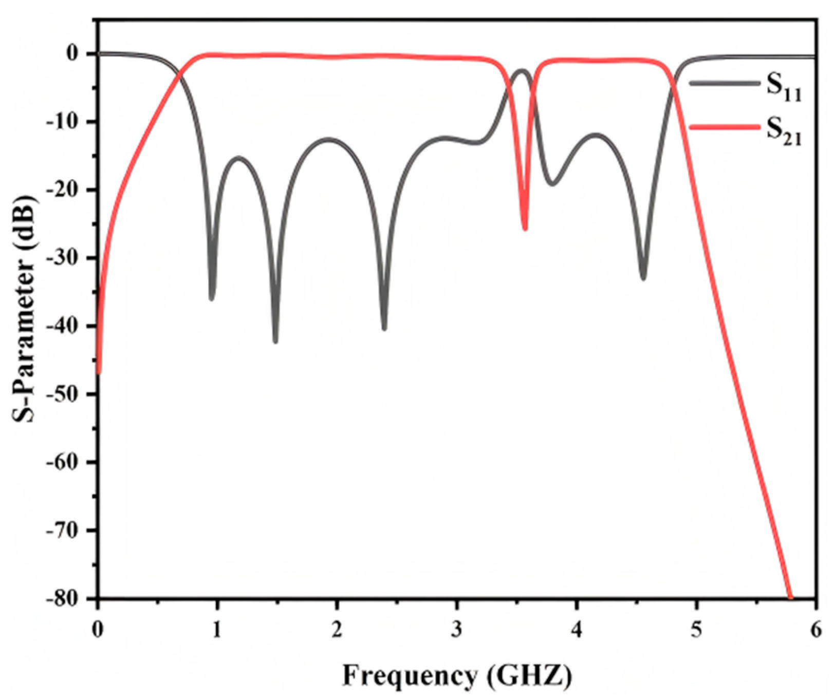
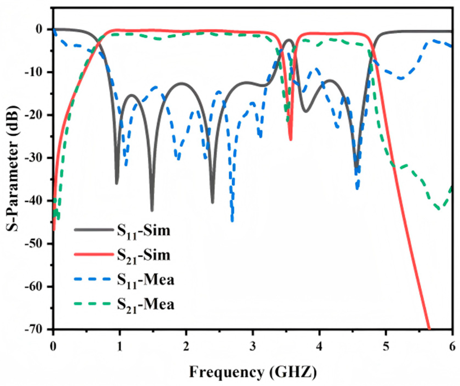
Figure 8 presents the simulated S-parameters of the proposed notch bandpass filter over the full frequency range. Two passbands are obtained from 0.67 to 3.40 GHz and from 3.67 to 4.77 GHz. The insertion loss is 0.48 dB at 2.00 GHz and 1.11 dB at 4.22 GHz. The return loss in both passbands remains better than −12 dB. In addition, the etched DGS introduces a deep notch centered at 3.50 GHz with a rejection level of −25 dB. A deep notch of −25 dB is achieved at 3.50 GHz to mitigate interference around the 3.5 GHz band, which is relevant to several wireless and radar related scenarios. These results confirm high in-band transmission and effective suppression at the specified frequency.
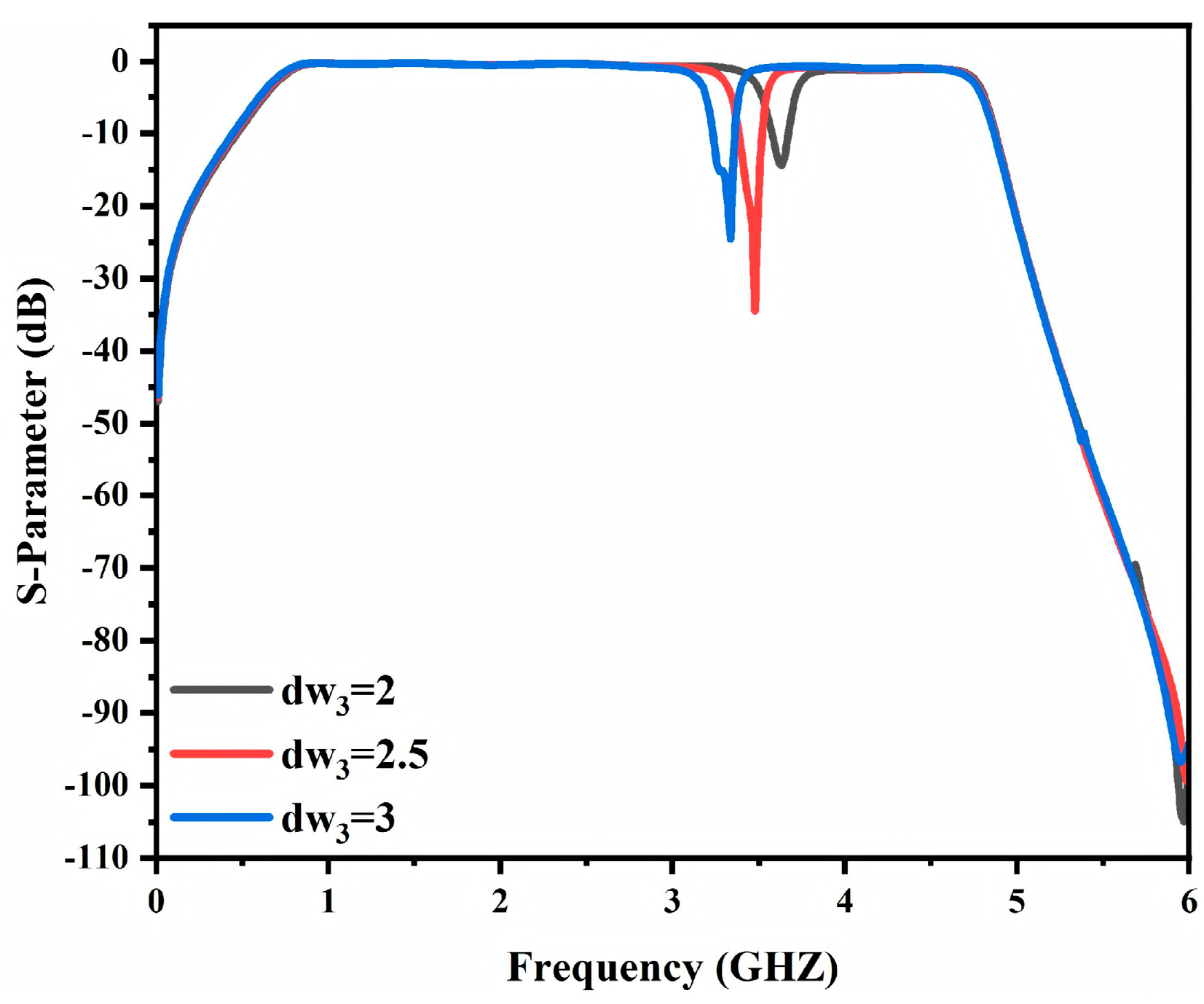
Furthermore, the dispersion-based analysis indicates that varying the effective area of the defected ground structure changes its equivalent inductance. This shifts the resonant frequency of the DGS and consequently tunes the notch frequency. As shown in
Figure 9, the notch location changes as the DGS parameter dw
3 is adjusted. When dw
3 increases from 2 mm to 3 mm, the notch frequency shifts from 3.6 GHz to 3.3 GHz. Therefore, the notch position can be precisely predefined during the design stage through appropriate selection of the DGS geometrical parameters to satisfy different application requirements. This feature enables a more adaptable bandpass filter design for suppressing designated interference frequencies.
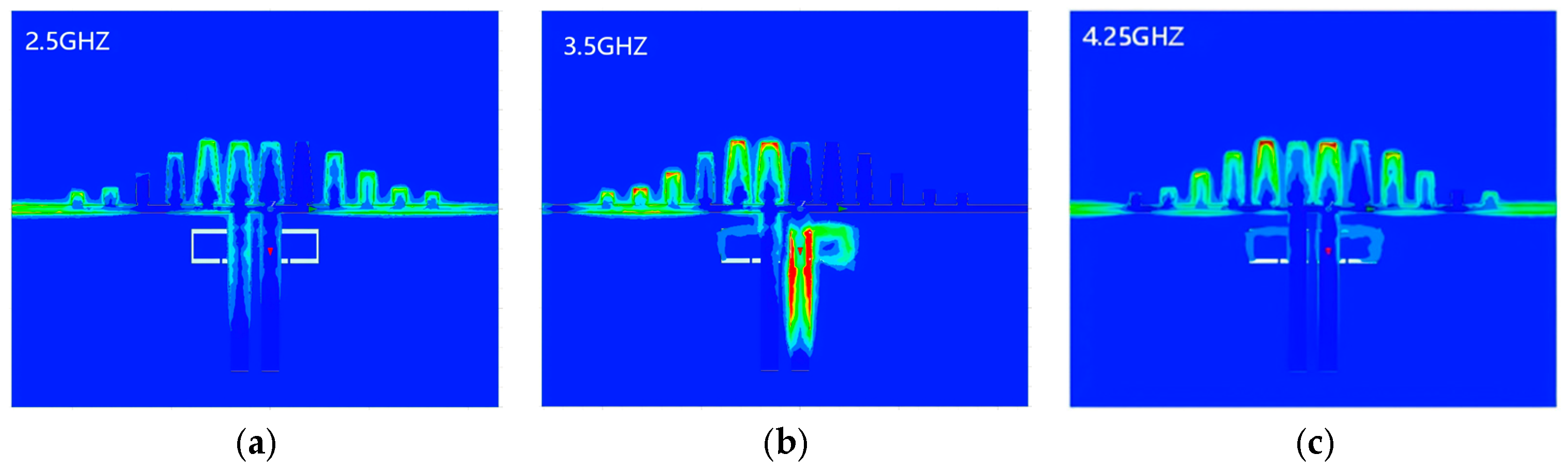
Figure 10 shows the simulated electric field distributions at representative frequencies to clarify the operating mechanism of the proposed notch bandpass filter. At 2.5 GHz and 4.25 GHz within the passband, the field is mainly confined along the transmission path and propagates with weak attenuation. In contrast, at 3.50 GHz, the field is strongly coupled to the defected ground structure and rapidly attenuated. This behavior indicates that the DGS introduces a resonant rejection at the notch frequency and suppresses wave transmission through the filter. Consequently, the 3.50 GHz component is effectively blocked, while the passband signals are maintained.