1. Introduction
Silicon carbide (SiC) Metal-Oxide-Semiconductor Field Effect Transistors (MOSFETs) are emerging as the most promising candidates for high-voltage and high-power applications [
1,
2,
3], which are attributed to their lower on-resistance, higher breakdown voltage, faster switching speed, and superior radiation resistance [
4,
5]. In power electronic modules such as DC-DC and AC-DC converters, the parasitic PN junction diode inherent in MOSFETs is employed to conduct a reverse current, serving as a cost-effective solution for freewheeling diode functionality [
6,
7,
8]. However, as a bipolar device, the parasitic PN junction diode injects a large number of carriers into the drift region during conduction. This leads to a substantial reverse recovery current and charge when the diode turns off, thereby significantly increasing the power loss in power electronic systems [
9].
In recent years, researchers have devoted greater efforts to addressing the abovementioned issue. The primary approach to solving this problem involves introducing unipolar diodes that are connected in parallel with a parasitic body PiN diode. The unipolar diode must possess a lower on-state voltage, when MOSFETs operate as freewheeling diodes, they conduct first, thereby significantly reducing the number of minority carriers injected into the drift region. Consequently, both the reverse recovery current and charge are greatly reduced. To summarize, there are three main types of such structures. The first is the Schottky Barrier Diode (SBD) [
10,
11,
12], the second is the built-in MOS-Channel Diode [
13,
14,
15], and the third is the heterojunction diode [
16,
17,
18].
However, the existing research has focused primarily on the 4H-SiC trench MOSFETs, with few studies examining the 4H-SiC LDMOS. Therefore, this paper explores a novel 4H-SiC LDMOS featuring a trench heterojunction diode to enhance reverse recovery performance. In recent years, the Si-SiC heterojunction LDMOS has been investigated to improve the trade-off between breakdown voltage and on-resistance [
19,
20,
21,
22,
23]. Nevertheless, in these works, the MOS portion of LDMOS is fabricated from silicon, while the substrate is composed of silicon carbide—a configuration that differs from the structure examined in this paper.
In this paper, a trench heterojunction diode is introduced into the source region of an LDMOS for the first time, positioned outside the main current conduction path of the device. The heterojunction diode, composed of P+ polysilicon and an N 4H-SiC drift region, is connected in parallel with a parasitic body diode and functions to suppress the conduction of the latter. The proposed device structure exhibits improved performance in terms of reverse recovery current and charge, while maintaining unchanged basic electrical characteristics such as transfer characteristics, output characteristics, and breakdown characteristics.
2. Device Structure and Operation Principle
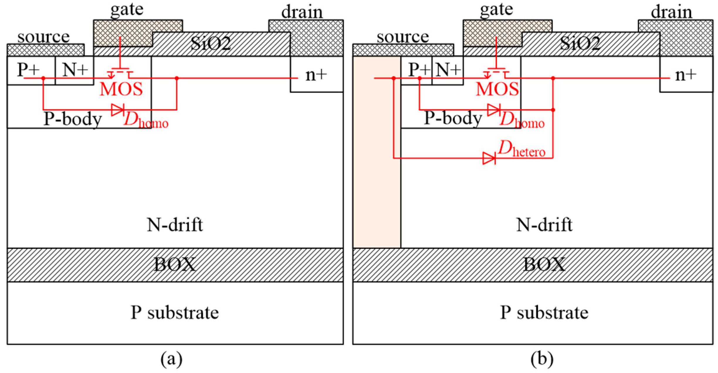
The structures of the conventional and proposed LDMOS are presented in
Figure 1a,b, abbreviated as C-LDMOS and THD-LDMOS, respectively. In addition,
Figure 1 illustrates the equivalent circuits of these two structures, each containing a parasitic P-body/N-drift junction diode that is connected in parallel with the LDMOS. Compared to a C-LDMOS, the THD-LDMOS is characterized by a trench heterojunction diode (THD) in the source side, which consists of P+ polysilicon and an N-drift region. The trench heterojunction diode, a unipolar device, is connected in parallel with the body PiN diode. When the LDMOS operates as a freewheeling diode, THD conducts first due to its lower on-state voltage, while simultaneously inhibiting the conduction of the body PiN diode. Consequently, the THD-LDMOS exhibits superior reverse recovery performance.
Figure 2 illustrates a band energy diagram of the homojunction and heterojunction diodes at thermal equilibrium. Silicon has a bandgap 1.1 of eV, approximately one-third of that of silicon carbide (3.24 eV). When a heterojunction is formed by P+ polysilicon and the 4H-SiC N-drift region, its built-in potential is approximately 0.77 V, whereas that of the 4H-SiC homojunction is about 2.88 V. Under zero bias, for both diodes, the valence band of P-type region is higher than that of the N-type region, preventing electrons in the valence band from moving from the N-type to the P-type region. Similarly, holes in the conduction band cannot migrate from the P-type to the N-type region.
A diode begins to conduct current when applied forward bias exceeds its built-in potential.
Figure 3 presents the band energy diagrams of the homojunction and heterojunction diodes under a forward bias voltage of 2.5 V—a voltage greater than that of the built-in potential of the heterojunction but lower than that of homojunction. In this scenario, the valence band of the P+ polysilicon region is lower than that of the 4H-SiC N-drift region, enabling electrons in the valence band to move from the N-type to the P-type region and form an electron current. However, no hole current is generated because the conduction band of the P+ polysilicon region is higher than that of the 4H-SiC N-drift region. Thus, the heterojunction diode, similar to a Schottky Barrier Diode (SBD), operates as a unipolar device, meaning only electron carriers exist in the 4H-SiC N-drift region. This characteristic contributes to its improved reverse recovery performance. As confirmed by
Figure 3a, the 4H-SiC homojunction diode remains off with no current flow when the forward bias is 2.5 V.
The C-LDMOS and THD-LDMOS share identical physical parameters, with the exception that a THD-LDMOS incorporates a trench P+ polysilicon region into its source. The P+ polysilicon trench has a depth and width of 4 μm and 2 μm, respectively. The gate oxide thickness is 30 nm, and the other parameters are listed in
Table 1.
3. Simulation Results and Discussion
In this section, the basic electrical characteristics are investigated in detail, including the transfer characteristics, output characteristics, and body diode performance. Additionally, when the LDMOS operates as a freewheeling diode, the reverse recovery characteristics of its parasitic diode are examined in depth.
3.1. Basic Electrical Characteristics
3.1.1. Transfer Characteristics
Figure 4 presents the transfer characteristics of the two structures, illustrating the relationship between the drain current density (
JD) and the gate voltage at a constant drain voltage, with the inset showing the test circuit for the transfer curves. As observed from this figure, both the C-LDMOS and THD-LDMOS exhibit a threshold voltage (
Vₜₕ) of approximately 5 V, which can be attributed to the identical parameters of their P-body regions.
3.1.2. Output Characteristics
Figure 5 presents a comparison of the output characteristics, illustrating the relationship between the drain current density (
JD) and the drain voltage under different gate voltages, with the inset showing the test circuit for the output curves. During normal operation of the device, current flows from the drain to the source along the upper surface of the N-drift region. Since the trench P+ polysilicon is positioned outside the current flow path, the THD-LDMOS exhibits the same current-driving capability and specific on-resistance as the C-LDMOS.
3.1.3. Breakdown Characteristics
Figure 6 illustrates the electric field distribution at a drain voltage of 600 V, where the electric field strength is close to the critical breakdown field of 4H-SiC material (3 MV/cm). Both devices undergo avalanche breakdown, indicating that their breakdown voltage is approximately 600 V. As shown in
Figure 6, the breakdown point is located on the drain side, while the trench heterojunction diode is positioned on the source side. Consequently, the THD-LDMOS and C-LDMOS exhibit identical voltage-withstanding capabilities.
3.2. Body Diode Characteristics
When the LDMOS functions as a freewheeling diode in converter applications, it is actually the parasitic body diode that acts as the freewheeling component. Therefore, it is desirable for the parasitic body diode to exhibit superior performance, such as a lower on-state voltage, lower reverse recovery current, and lower reverse recovery charge. However, the parasitic body PiN diode in the C-LDMOS is a bipolar device, which results in poor reverse recovery characteristics. Additionally, due to the higher built-in potential of the 4H-SiC diode, it has a higher on-state voltage. In contrast, the proposed structure adopts a trench heterojunction diode connected in parallel with the PiN diode, leading to improved performance.
Figure 7 presents a comparison of the performance of the parasitic body diodes in the C-LDMOS and THD-LDMOS, illustrating the relationship between the diode current density and the forward-bias voltage. To obtain the volt–ampere characteristics of the body diode, the inset of
Figure 7 shows the corresponding test circuit. The anode of the diode is connected to the source of the LDMOS, and the cathode is connected to the drain; thus, the source–drain voltage (
VSD) must be negative to forward-bias the diode. As shown in
Figure 7, the THD-LDMOS exhibits a lower on-state voltage when the diode current density is below 70 A/cm
2.
For instance, when the drain current density (
JD) is 50 A/cm
2, the on-state voltage of the THD-LDMOS is approximately 2.4 V, representing a 20% reduction compared to the C-LDMOS. The primary reason for this phenomenon is illustrated in
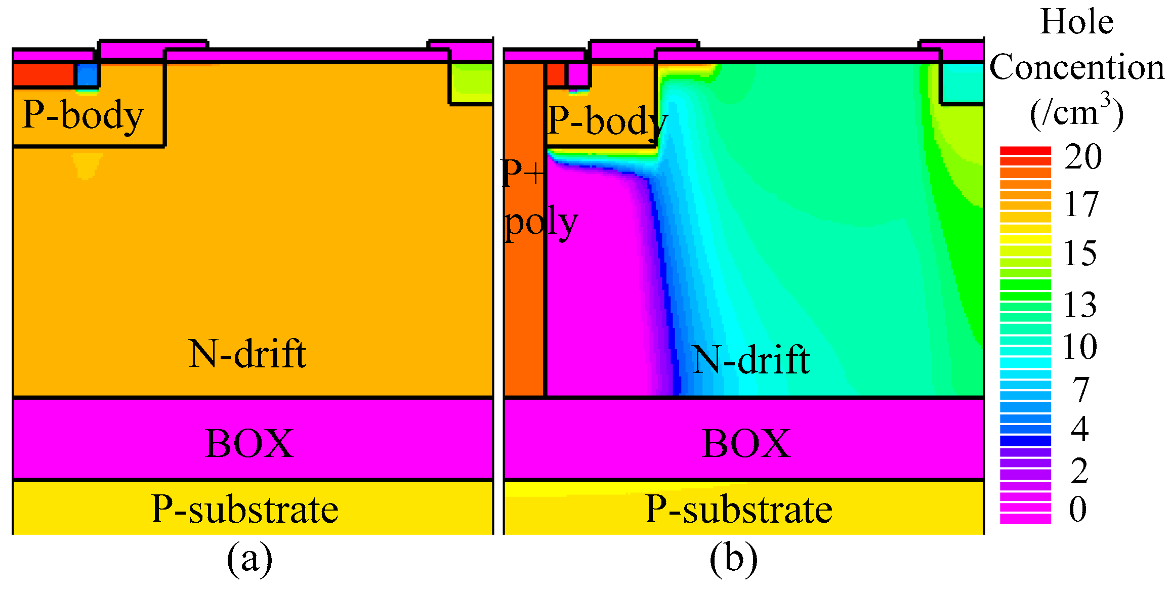
Figure 8,
Figure 9 and
Figure 10. The distributions of electrons (
Figure 8) and holes (
Figure 9) demonstrate that the trench heterojunction diode suppresses the conduction of the body PiN diode. Furthermore, the distribution of current flowlines (
Figure 10) further confirms the aforementioned conclusion, as these flowlines are confined exclusively to the trench heterojunction diode.
As the forward current increases, the carrier concentration in the N-drift region of the C-LDMOS also rises, since its body diode is a bipolar device. In contrast, the carrier concentration in the THD-LDMOS remains approximately constant because its heterojunction diode operates as a unipolar device. An increase in the carrier concentration of the N-drift region leads to a reduction in its parasitic equivalent resistance. As a result, the forward on-state voltage of the proposed device (THD-LDMOS) becomes larger than that of the conventional device (C-LDMOS) under higher current conditions.
3.3. Reverse Recovery Characteristics
The reverse recovery performance of the parasitic diode exerts a significant influence on electronic systems utilizing an LDMOS. The test circuit is presented in
Figure 11a, where a resistor and a current source are connected in parallel to control the anode voltage of the diode (the source voltage of the LDMOS). In a static state, the resistor value is 20 Ω, resulting in an anode voltage of 200 V for the parasitic diode—a value higher than the cathode voltage (or drain voltage) of 100 V—thus placing the parasitic diode in an on-state. Subsequently, the resistor value is reduced from 20 Ω to 0 Ω, causing the anode voltage of the parasitic diode to drop from 200 V to 0 V, which simulates the reverse recovery process of the diode.
The reverse recovery characteristics of the C-LDMOS and THD-LDMOS are presented in
Figure 11b. As shown in this figure, the THD-LDMOS exhibits a lower reverse recovery peak current (
IRM) of approximately 117 A/cm
2, representing a 55.5% reduction compared to the C-LDMOS, which has a value of about 263 A/cm
2. Additionally, the reverse recovery charge (
QRR) can be derived by integrating the current over time. For the THD-LDMOS and C-LDMOS, the
QRR values are approximately 2.47 μC/cm
2 and 11.05 μC/cm
2, respectively, corresponding to a 77.7% reduction in the THD-LDMOS.
Figure 12 and
Figure 13 illustrate the electron and hole concentrations in the C-LDMOS and THD-LDMOS, respectively. As shown in
Figure 12, at the same current density, the THD-LDMOS exhibits a lower electron concentration in the N-drift region, on the order of 10
15 cm
−3 (shown in
Figure 14). This is 100 times smaller than the electron concentration in the C-LDMOS, which is on the order of 10
17 cm
−3 (shown in
Figure 14). In contrast,
Figure 13 reveals that the C-LDMOS contains a large number of hole carriers in the N-drift region, generated by the conduction of its parasitic PiN diode. As observed in
Figure 7, although the on-state voltage of the parasitic diode in the THD-LDMOS is slightly higher than that in the C-LDMOS, its reverse recovery performance is significantly improved. This is because the trench heterojunction diode integrated into the THD-LDMOS is a unipolar device, endowing the THD-LDMOS with superior reverse recovery characteristics.
4. Conclusions
To enhance the reverse recovery performance of the conventional 4H-SiC LDMOS, this paper proposes a novel LDMOS device, incorporating a unipolar trench heterojunction formed by P+ polysilicon and a 4H-SiC N-drift region. For the first time, the reverse recovery characteristics of a Si/SiC LDMOS are investigated in detail. To avoid the degradation of basic electrical characteristics, the trench Si/SiC heterojunction is introduced in the source region, positioned outside the main current flow path. In summary, the proposed THD-LDMOS exhibits improved reverse recovery performance, and a lower on-state voltage for the diode compared to the C-LDMOS. Simulation results indicate that at a current density of 100 A/cm2, the THD-LDMOS achieves a reverse recovery peak current of 117 A/cm2 and a reverse recovery charge of 2.47 μC/cm2, representing reductions of 55.5% and 77.7%, respectively, relative to the C-LDMOS.
Author Contributions
Conceptualization, Y.L. and F.B.; Investigation, Y.L. and J.F.; Methodology, J.F.; Software, Y.L. and F.B.; Validation, Y.L. and J.F.; Writing—original draft, Y.L.; Writing—review and editing, Y.L., F.B. and J.F. All authors have read and agreed to the published version of the manuscript.
Funding
This research was funded by the 2025 Project of the Liaoning Provincial Department of Education (I have not received a number for this grant), and in part, by the PhD research startup foundation of Shenyang Aerospace University, grant number 19YB47.
Data Availability Statement
The original contributions presented in this study are included in the article. Further inquiries can be directed to the corresponding author.
Conflicts of Interest
The authors declare no conflicts of interest.
References
- Spitz, J.; Melloch, M.; Cooper, J.; Capano, M. 2.6 kV 4H-SiC Lateral DMOSFETs. IEEE Electron. Device Lett. 1998, 19, 100–102. [Google Scholar] [CrossRef]
- Kong, M.; Hu, Z.; Gao, J.; Chen, Z.; Zhang, B.; Yang, H. A 1200-V-Class Ultra-Low Specific On-Resistance SiC Lateral MOSFET with Double Trench Gate and VLD Technique. IEEE J. Electron. Devices Soc. 2021, 10, 83–88. [Google Scholar] [CrossRef]
- Hu, Z.; Yao, J.; Li, A.; Sun, Q.; Li, M.; Yang, K.; Zhang, J.; Chen, J.; Zhang, M.; Guo, Y. Review of the SiC LDMOS Power Device. J. Semicond. 2024, 45, 081501. [Google Scholar] [CrossRef]
- Mao, S.; Popovic, J.; Ferreira, J.A. Efficiency impacts of 1.2kV silicon carbide MOSFETs for isolated two-stage AC-DC power conversion. In Proceedings of the 1st Workshop on Wide Bandgap Power Devices and Applications in Asia, Xi’an, China, 16–18 May 2018. [Google Scholar]
- Funaki, T.; Matsushita, M.; Sasagawa, M.; Kimoto, T.; Hikihara, T. A study on SiC devices in synchronous rectification of DC-DC converter. In Proceedings of the 22nd Annual IEEE Applied Power Electronics Conference (APEC 2007), Anaheim, CA, USA, 25 February–1 March 2007. [Google Scholar]
- Zeng, J.; Wheatley, C.F.; Stokes, R.; Kocon, C.; Benczkowski, S. Optimization of the body-diode of power MOSFETs for high efficiency synchronous rectification. In Proceedings of the 12th International Symposium on Power Semiconductor Devices & ICs. Proceedings, Toulouse, France, 22–25 May 2000. [Google Scholar]
- Chen, P.Y.; Jinno, M.; Shie, Y.M. Research on the reverse conduction of synchronous rectifiers. IEEE Trans. Ind. Electron. 2008, 55, 1570–1575. [Google Scholar] [CrossRef]
- Napoli, E.; Spirito, P.; Strollo, A.G.M.; Frisina, F.; Fragapane, L.; Fagone, D. Design of IGBT with integral freewheeling diode. IEEE Electron. Device Lett. 2002, 23, 532–534. [Google Scholar] [CrossRef]
- Ren, Y.; Xu, M.; Zhou, J.; Lee, F. Analytical loss model of power MOSFET. IEEE Trans. Power Electron. 2006, 21, 310–319. [Google Scholar] [CrossRef]
- Han, Z.; Bai, Y.; Chen, H.; Li, C.; Lu, J.; Song, G.; Liu, X. A trench/planar SiC MOSFET integrated with SBD (TPSBD) for low reverse recovery charge and low switching loss. Semicond. Sci. Technol. 2020, 35, 105002. [Google Scholar] [CrossRef]
- Cao, W.; Ying, S.; Ge, X.; Liu, D. SiC superjunction MOSFET with Schottky diode for improving short-circuit and reverse recovery ruggedness. Micro Nanostructures 2024, 191, 207847. [Google Scholar] [CrossRef]
- Liu, S.; Tang, X.; Song, Q.; Wang, Y.; Bai, R.; Zhang, Y.; Zhang, Y. A novel SiC trench MOSFET with integrated Schottky barrier diode for improved reverse recovery charge and switching loss. IET Power Electron. 2021, 14, 2021–2026. [Google Scholar] [CrossRef]
- Huang, M.; Li, R.; Yang, Z.; Ma, Y.; Li, Y.; Zhang, X.; Gong, M. A Multiepi Superjunction MOSFET with a Lightly Doped MOS-Channel Diode for Improving Reverse Recovery. IEEE Trans. Electron. Devices 2021, 68, 2401–2407. [Google Scholar] [CrossRef]
- Zhang, M.; Wei, J.; Zhou, X.; Jiang, H.; Li, B.; Chen, K.J. Simulation Study of a Power MOSFET with Built-in Channel Diode for Enhanced Reverse Recovery Performance. IEEE Electron. Device Lett. 2019, 40, 79–82. [Google Scholar] [CrossRef]
- Li, P.; Guo, J.; Lin, Z.; Hu, S. A Power MOSFET with P-Base Schottky Diode and Built-In Channel Diode for Fast Reverse Recovery. IEEE J. Electron. Devices Soc. 2021, 9, 300–305. [Google Scholar] [CrossRef]
- Kim, J.; Kim, K. A Novel 4H-SiC Super Junction UMOSFET with Hetero-Junction Diode for Enhanced Reverse Recovery Char-acteristics and Low Switching Loss. Semiconductors 2020, 54, 587–595. [Google Scholar] [CrossRef]
- Kim, J.; Kim, K. 4H-SiC Double-Trench MOSFET with Side Wall Heterojunction Diode for Enhanced Reverse Recovery Performance. Energies 2020, 13, 4602. [Google Scholar] [CrossRef]
- Yang, T.; Wang, Y.; Yue, R. A heterojunction-based SiC power double trench MOSFET with improved switching performance and reverse recovery. Superlattices Microstruct. 2020, 140, 106466.1–106466.6. [Google Scholar] [CrossRef]
- Wang, N.; Hu, X.; Xu, Y.; Li, T. A Triple RESURF Si/SiC HeteroJunction LDMOS and Its Analytical Model. Int. J. Numer. Model.-Electron. Netw. Devices Field 2025, 38, e70039. [Google Scholar] [CrossRef]
- Duan, B.; Huang, X.; Song, H.; Wang, Y.; Yang, Y. Novel Si/SiC Heterojunction Lateral Double-diffused Metal Oxide Semiconductor Field Effect Transistor with P-type Buried Layer Breaking Silicon Limit. Chin. Phys. B 2020, 30, 048503. [Google Scholar] [CrossRef]
- Li, Q.; Yuan, L.; Zhang, F.; Li, H.; Xiao, G.; Chen, Y.; Sun, T.; Liu, X.; Fu, T. Novel SiC/Si heterojunction LDMOS with electric field modulation effect by reversed L-shaped field plate. Results Phys. 2025, 16, 102837. [Google Scholar] [CrossRef]
- Wang, Y.; Duan, B.; Sun, L.; Yang, X.; Huang, Y.; Yang, Y. Breakdown Point Transfer Theory for Si/SiC Heterojunction LDMOS with Deep Drain Re-gion. Superlattices Microstruct. 2021, 151, 106810. [Google Scholar] [CrossRef]
- Duan, B.; Xue, S.; Huang, X.; Yang, Y. Novel Si/SiC Heterojunction Lateral Double-Diffused Metal Oxide Semiconductor with SIPOS Field Plate by Simulation Study. IEEE J. Electron. Devices Soc. 2021, 9, 114–120. [Google Scholar] [CrossRef]
| Disclaimer/Publisher’s Note: The statements, opinions and data contained in all publications are solely those of the individual author(s) and contributor(s) and not of MDPI and/or the editor(s). MDPI and/or the editor(s) disclaim responsibility for any injury to people or property resulting from any ideas, methods, instructions or products referred to in the content. |
© 2025 by the authors. Licensee MDPI, Basel, Switzerland. This article is an open access article distributed under the terms and conditions of the Creative Commons Attribution (CC BY) license (https://creativecommons.org/licenses/by/4.0/).


