
Design of a Current-Mode OTA-Based Memristor Emulator for Neuromorphic Medical Application


Abstract
1. Introduction
2. Design of the Emulator
2.1. Characteristics
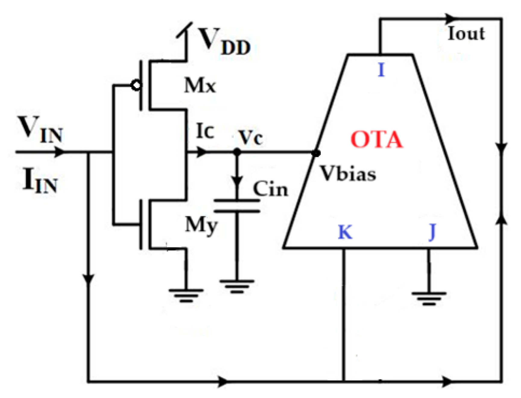
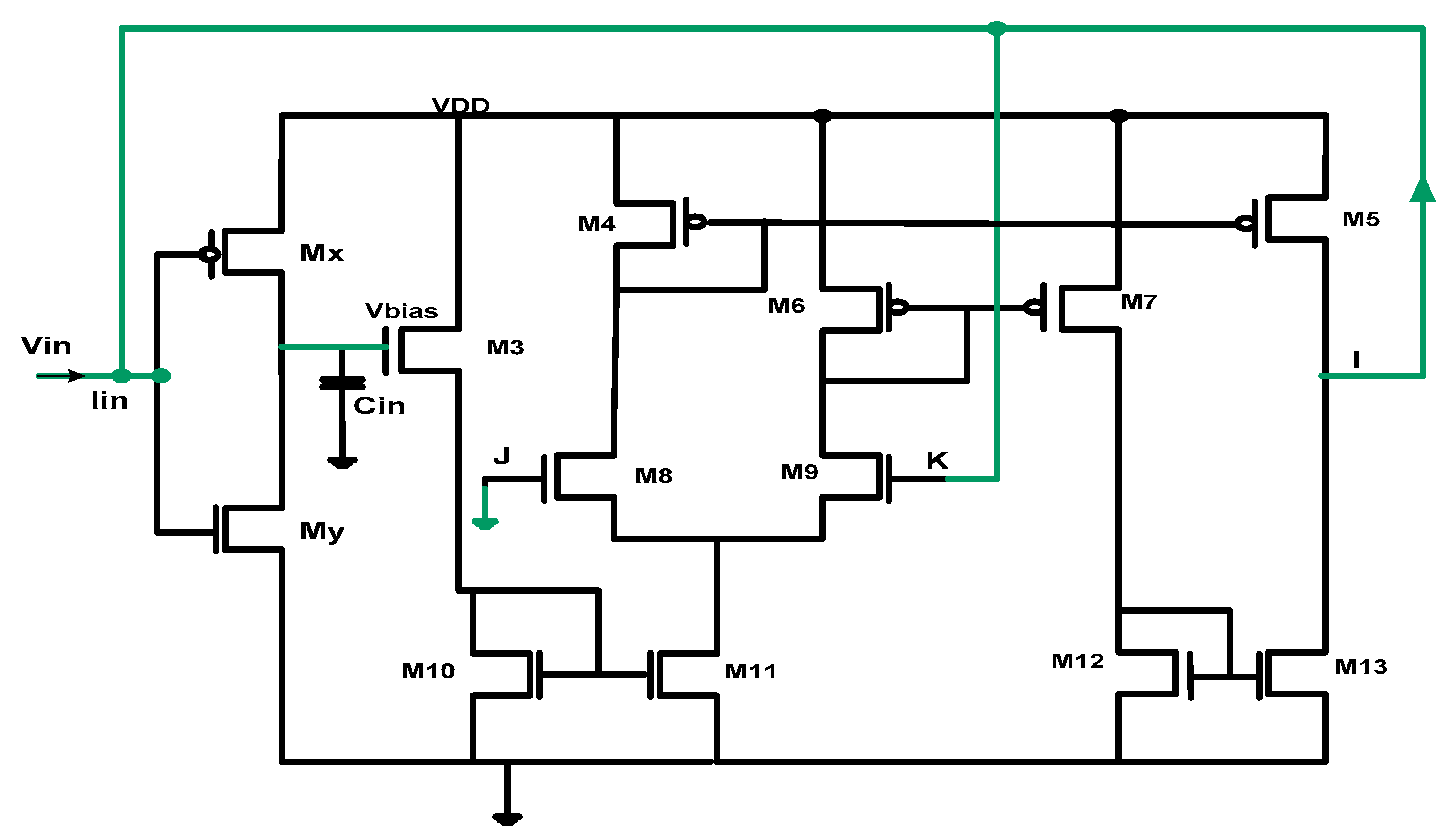
2.2. Circuit Description and Mathematical Modeling
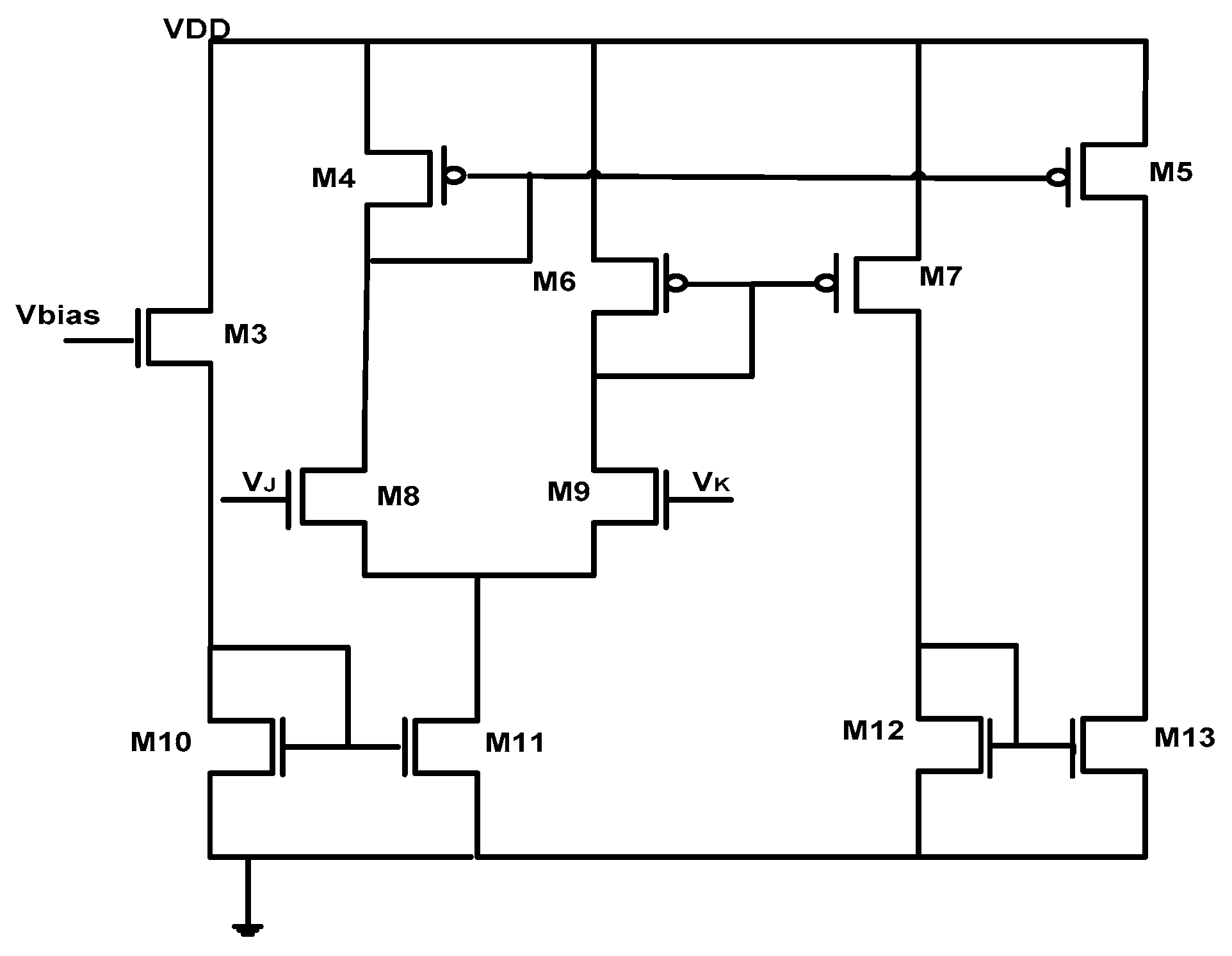
2.3. OTA Design
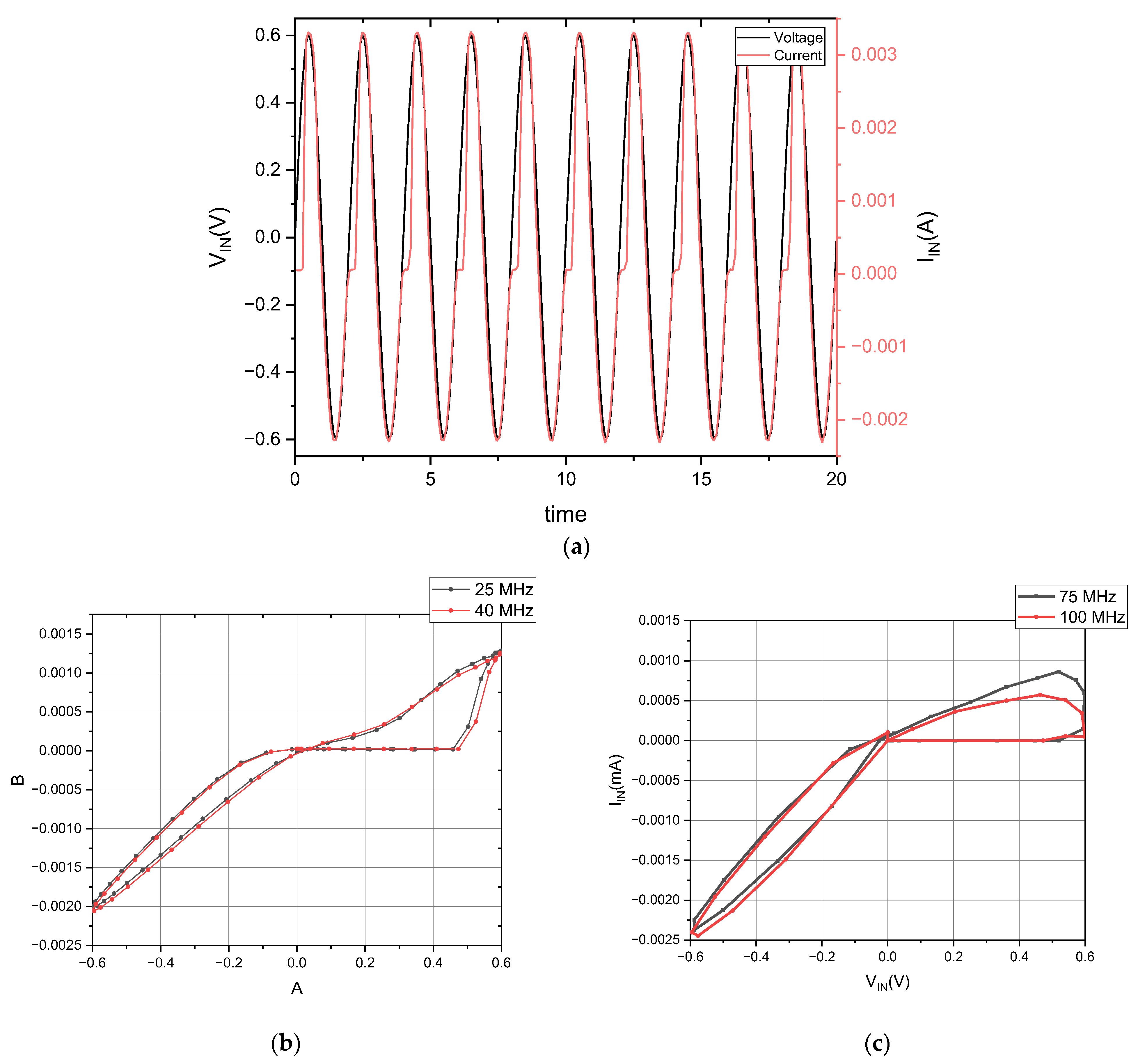
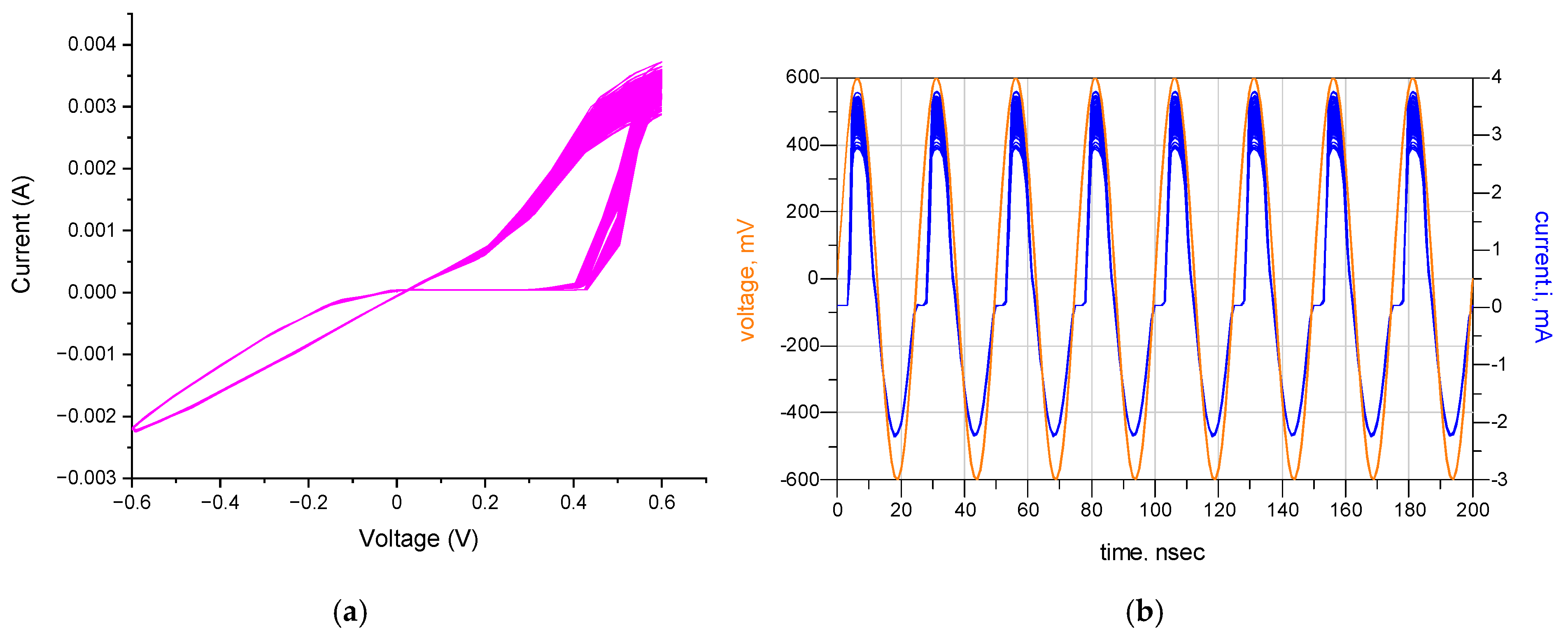
3. Results and Discussion
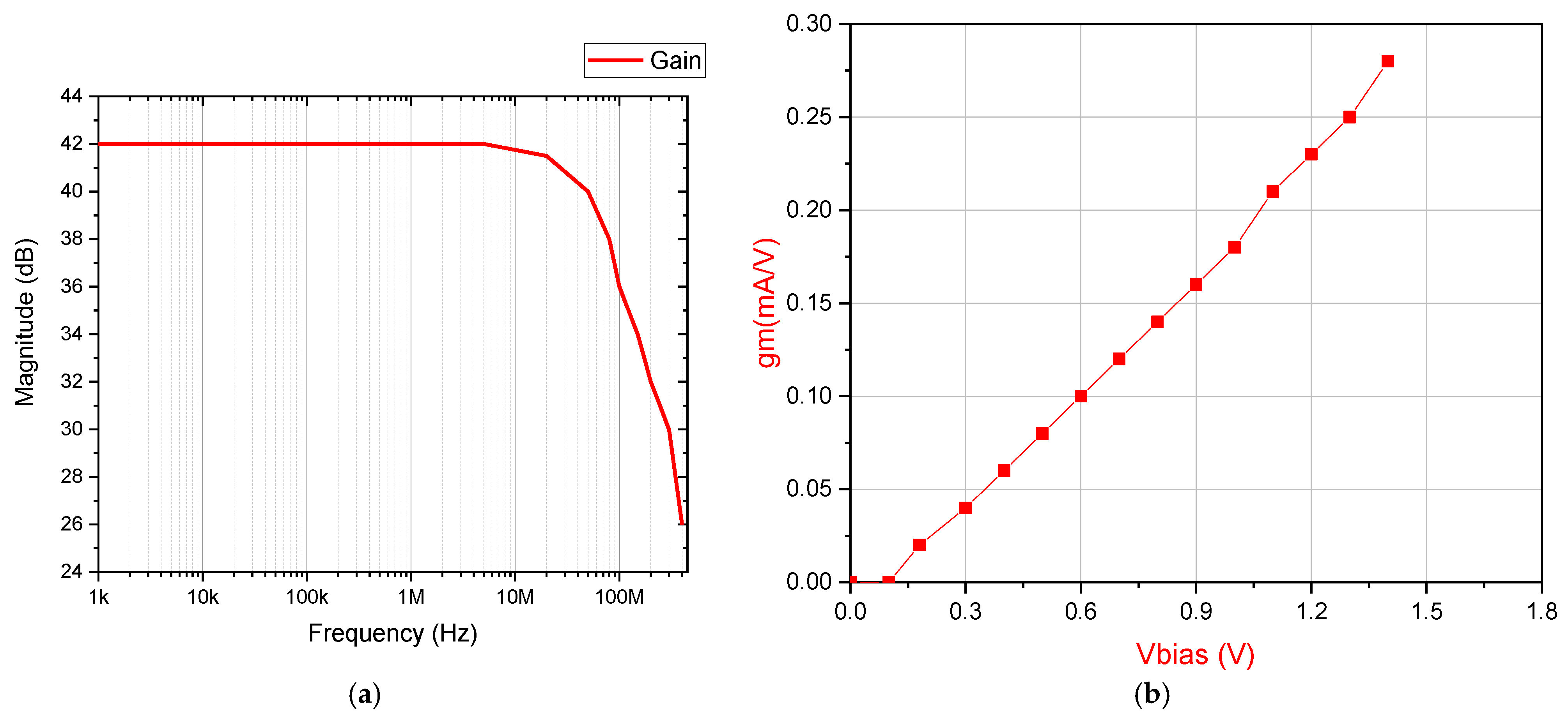
3.1. Simulation Results
3.2. Comparison
- High-Frequency Performance: The proposed emulator achieves a high operating frequency of 100 MHz, matching the highest performance reported in the literature [32], while offering significant architectural improvements. Unlike the reference design requiring 15 MOS transistors and a differential voltage current conveyor (DVCC) with three additional MOS devices, our implementation attains this high-frequency operation with greater efficiency, utilizing only 13 transistors in total and a simpler configuration based on a single OTA with just two MOS components.
- Compact and Efficient Design: The proposed design uses only 13 transistors, fewer than most reported works: 27 in [28], 24 in [15], 32 in [30], 34 in [33], and 22 in [34]. Additionally, it requires just one active block (OTA) and one capacitor, reducing passive component count compared to designs using resistors like [28,30,33].
- Power Efficiency: The design achieves enhanced power efficiency through three key features: a simplified circuit implementation that minimizes both static and dynamic power consumption; avoidance of DC offset circuitry, as transistor polarization is maintained in the required operating region through careful biasing; and adoption of an asymmetric power supply scheme (0 V to 1.2 V) to further optimize energy efficiency. These architectural choices collectively enable significant power savings while preserving the circuit’s memristive functionality.
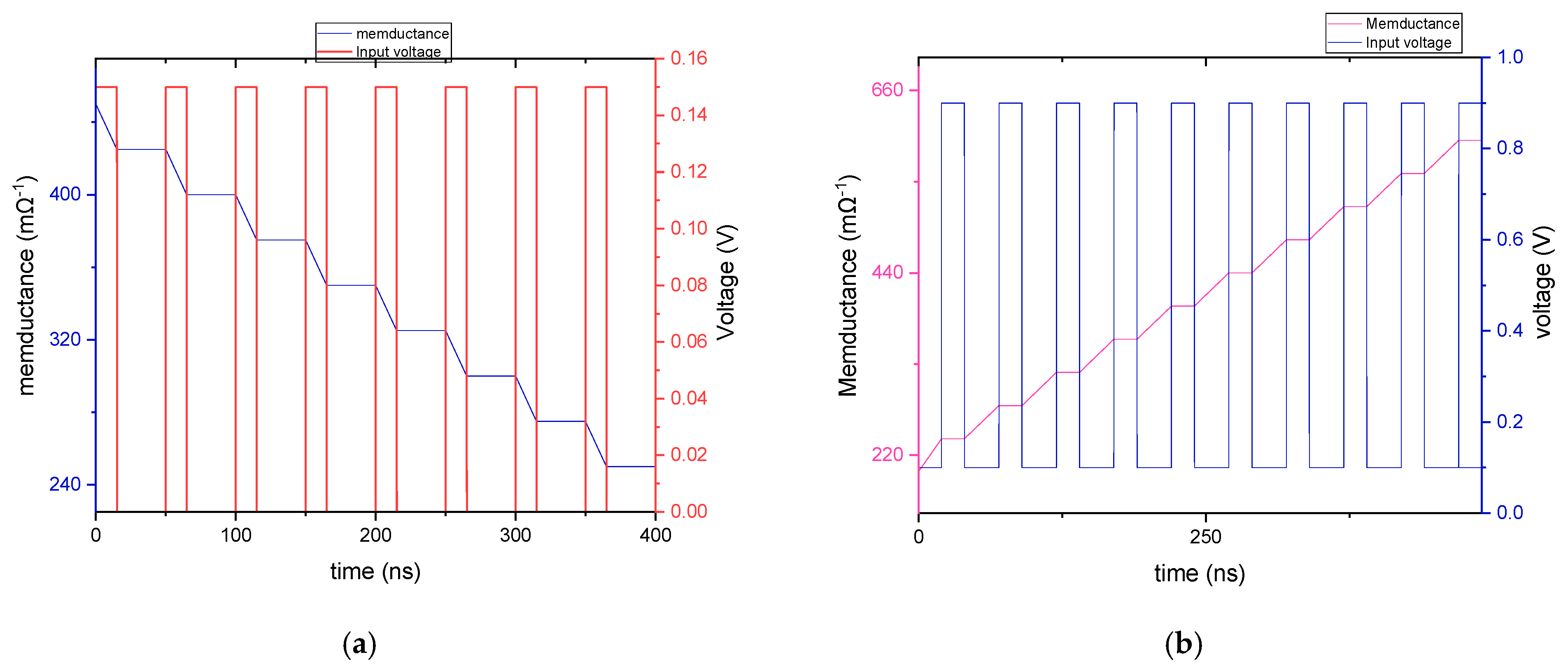
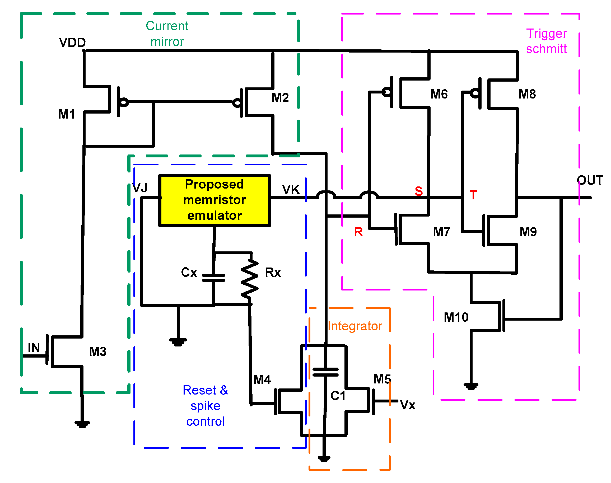
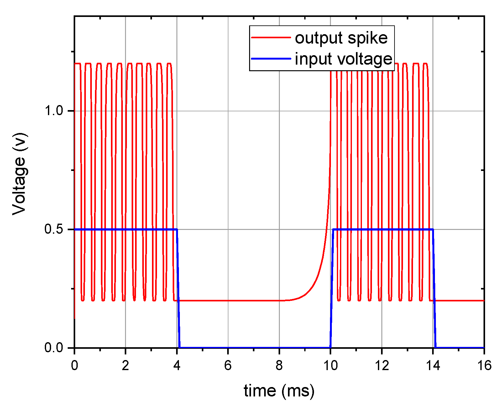
4. Application: MIF Neuron Circuit for Retinal Protheses
4.1. Memristive Integrate and Fire (MIF) Neuron Circuit
4.2. Adaptive MIF Neuron for Artificial Retina Design
4.3. Results and Discussion
5. Conclusions
Author Contributions
Funding
Data Availability Statement
Acknowledgments
Conflicts of Interest
References
- Chua, L. Memristor—The missing circuit element. IEEE Trans. Circuit Theory 1971, 18, 507–519. [Google Scholar] [CrossRef]
- Chua, L.O.; Kang, S.M. Memristive devices and systems. Proc. IEEE 1976, 64, 209–223. [Google Scholar] [CrossRef]
- Barraj, I.; Mestiri, H.; Masmoudi, M. Overview of Memristor-Based Design for Analog Applications. Micromachines 2024, 15, 505. [Google Scholar] [CrossRef] [PubMed]
- Prasad, S.S.; Kumar, P.; Raj, N.; Sharma, P.K.; Priyadarshini, B.; Ranjan, R.K.; Prommee, P. A compact floating and grounded memristor model using single active element. AEU-Int. J. Electron. Commun. 2022, 157, 154426. [Google Scholar] [CrossRef]
- Strukov, D.B.; Snider, G.S.; Stewart, D.R.; Williams, R.S. The missing Memristor found. Nature 2008, 453, 80–83. [Google Scholar] [CrossRef] [PubMed]
- Vongehr, S.; Meng, X. The Missing Memristor has Not been Found. Sci. Rep. 2015, 5, 11657. [Google Scholar] [CrossRef] [PubMed]
- Batas, D.; Fiedler, H. A memristor SPICE implementation and a new approach for magnetic flux-controlled memristor modeling. IEEE Trans. Nanotechnol. 2011, 10, 250–255. [Google Scholar] [CrossRef]
- Sánchez López, C.; Carrasco Aguilar, M.A.; Muñiz Montero, C. A 16 Hz–160 kHz memristor emulator circuit. AEU-Int. J. Electron. Commun. 2015, 69, 1208–1219. [Google Scholar] [CrossRef]
- Ranjan, R.K.; Sharma, P.K.; Sagar; Raj, N.; Kumari, B.; Khateb, F. Memristor emulator circuit using multiple-output OTA and its experimental results. J. Circuits Syst. Comput. 2019, 28, 1950166. [Google Scholar] [CrossRef]
- Ranjan, R.K.; Raj, N.; Bhuwal, N.; Khateb, F. Single DVCCTA based high frequency incremental/decremental memristor emulator and its application. AEU-Int. J. Electron. Commun. 2017, 82, 177–190. [Google Scholar] [CrossRef]
- Pershin, Y.V.; Sazonov, E.; Di Ventra, M. Analogue-to-digital and digital-to-analogue conversion with memristive devices. Electron. Lett. 2012, 48, 73–74. [Google Scholar] [CrossRef]
- Bhardwaj, K.; Srivastava, M. New electronically adjustable memelement emulator for realizing the behaviour of ful-ly-floating meminductor and memristor. Microelectron. J. 2021, 114, 105126. [Google Scholar] [CrossRef]
- Prasad, S.S.; Ranjan, R.K.; Kang, S.-M. Resistorless floating/grounded memristor emulator model with electronic tunability. IEEE Trans. Circuits Syst. II Exp. Briefs 2023, 70, 2340–2344. [Google Scholar]
- Sánchez-López, C.; Aguila-Cuapio, L. A 860 kHz grounded memristor emulator circuit. AEU-Int. J. Electron. Commun. 2017, 73, 23–33. [Google Scholar] [CrossRef]
- Raj, N.; Ranjan, R.K.; Khateb, F. Flux-controlled memristor emulator and its experimental results. IEEE Trans. Very Large Scale Integr. Syst. 2020, 28, 1050–1061. [Google Scholar] [CrossRef]
- Antolini, A.; Lico, A.; Scarselli, E.F.; Carissimi, M.; Pasotti, M. Phase-Change Memory Cells Characterization in an Analog In-Memory Computing Perspective. In Proceedings of the 2022 17th Conference on Ph.D Research in Microelectronics and Electronics (PRIME), Villasimius, Italy, 12–15 June 2022; pp. 233–236. [Google Scholar] [CrossRef]
- Mladenov, V. A modified tantalum oxide memristor model for neural networks with memristor-based synapses. In Proceedings of the 9th International Conference on Modern Circuits and Systems Technologies (MOCAST), Bremen, Germany, 7–9 September 2020; pp. 1–4. [Google Scholar]
- Mladenov, V. Analysis and simulations of hybrid memory scheme based on memristors. Electronics 2018, 7, 289. [Google Scholar] [CrossRef]
- Kumar, P.; Ranjan, R.K.; Kang, S.-M. A Memristor Emulation in 180-nm CMOS Process for Spiking Signal Generation and Chaos Application. IEEE Trans. Circuits Syst. I Regul. Pap. 2024, 71, 1757–1770. [Google Scholar] [CrossRef]
- Ghosh, M.; Singh, A.; Borah, S.S.; Vista, J.; Ranjan, A.; Kumar, S. MOSFET-based memristor for high-frequency signal processing. IEEE Trans. Electron Devices 2022, 69, 2248–2255. [Google Scholar] [CrossRef]
- Barraj, I.; Neifar, A.; Mestiri, H.; Masmoudi, M. Zero-Power, High-Frequency Floating Memristor Emulator Circuit and Its Applications. Micromachines 2025, 16, 269. [Google Scholar] [CrossRef] [PubMed]
- Babacan, Y.; Yesil, A.; Gul, F. The Fabrication and MOSFET-Only Circuit Implementation of Semiconductor Memristor. IEEE Trans. Electron Devices 2018, 65, 1625–1632. [Google Scholar] [CrossRef]
- Yang, S.; Liu, B.; Li, W.; Wu, D.; He, Y.; Dai, G. Design and Application of Passive Very High-Frequency Memristor Emulator. Circuits Syst. Signal Process. 2024, 44, 2330–2348. [Google Scholar] [CrossRef]
- Samardzic, N.M.; Bajic, J.S.; Sekulic, D.L.; Dautovic, S. Volatile Memristor in Leaky Integrate-and-Fire Neurons: Circuit Simulation and Experimental Study. Electronics 2022, 11, 894. [Google Scholar] [CrossRef]
- Singh, P.P.; Roy, B.K.; Volos, C. Memristor-based novel 4D chaotic system without equilibria: Analysis and projective synchronization. In Mem-Elements for Neuromorphic Circuits with Artificial Intelligence Applications; Academic Press: New York, NY, USA, 2021; pp. 183–205. [Google Scholar]
- Adhikari, S.P.; Sah, M.P.; Kim, H.; Chua, L.O. Three fingerprints of memristor. In Handbook of Memristor Networks; Springer: Cham, Switzerland, 2019; pp. 165–196. [Google Scholar]
- Raj, N.; Ranjan, R.K. Emulation of novel floating and tunable Multimem-Elements circuit and its application. AEU-Int. J. Electron. Commun. 2024, 177, 155215. [Google Scholar] [CrossRef]
- Prasad, S.S.; Raj, N.; Verma, V.K.; Ranjan, R.K. Electronically tunable flux-controlled resistorless memristor emulator. IEEE Can. J. Electr. Comput. Eng. 2022, 45, 311–317. [Google Scholar] [CrossRef]
- Yeşil, A.; Babacan, Y.; Kaçar, F. Design and experimental evolution of memristor with only one VDTA and one capacitor. IEEE Trans. Comput. Des. Integr. Circuits Syst. 2018, 38, 1123–1132. [Google Scholar] [CrossRef]
- Petrovic, P.B. Floating incremental/decremental flux-controlled memristor emulator circuit based on single VDTA. Analog. Integr. Circuits Signal Process. 2018, 96, 417–733. [Google Scholar] [CrossRef]
- Vista, J.; Ranjan, A. Flux controlled floating memristor employing VDTA: Incremental or decremental operation. IEEE Trans. Comput. Des. Integr. Circuits Syst. 2020, 40, 364–372. [Google Scholar] [CrossRef]
- Sharma, P.K.; Ranjan, R.K. Single DVCC based High Frequency Flux Controlled Memristor Emulator and its Experimental Results. Res. Sq. 2022, preprint. [Google Scholar] [CrossRef]
- Ersoy, D.; Kaçar, F. Electronically Charge-Controlled Tunable Meminductor Emulator Circuit With OTAs and Its Applications. IEEE Access 2023, 11, 53290–53300. [Google Scholar] [CrossRef]
- Singh, A.; Rai, S.K. VDCC-Based Memcapacitor/Meminductor Emulator and Its Application in Adaptive Learning Circuit. Iran. J. Sci. Technol. Trans. Electr. Eng. 2021, 45, 1151–1163. [Google Scholar] [CrossRef]
- Lin, Z.; Zhang, S.; Jin, Q.; Xia, J.; Liu, Y.; Yu, K.; Zheng, J.; Xu, X.; Fan, X.; Li, K.; et al. A Fully Digital SRAM-Based Four-Layer In-Memory Computing Unit Achieving Multiplication Operations and Results Store. IEEE Trans. Very Large Scale Integr. Syst. 2023, 31, 776–788. [Google Scholar] [CrossRef]
- Bankman, D.; Messner, J.; Gural, A.; Murmann, B. RRAM-Based In-Memory Computing for Embedded Deep Neural Networks. In Proceedings of the 2019 53rd Asilomar Conference on Signals, Systems, and Computers, Pacific Grove, CA, USA, 3–6 November 2019; pp. 1511–1515. [Google Scholar] [CrossRef]
- Shamsi, J.; Mohammadi, K.; Shokouhi, S.B. A hardware architecture for columnar-organized memory based on CMOS neuron and memristor crossbar arrays. IEEE Trans. Very Large Scale Integr. Syst. 2018, 26, 2795–2805. [Google Scholar] [CrossRef]
- Wang, Q.; Pan, G.; Jiang, Y. An Ultra-Low Power Threshold Voltage Variable Artificial Retina Neuron. Electronics 2022, 11, 365. [Google Scholar] [CrossRef]
- Aboumerhi, K.; Güemes, A.; Liu, H.; Tenore, F.; Etienne-Cummings, R. Neuromorphic applications in medicine. J. Neural Eng. 2023, 20, 041004. [Google Scholar] [CrossRef] [PubMed]
- Fang, X.; Duan, S.; Wang, L. Memristive Hodgkin-Huxley Spiking Neuron Model for Reproducing Neuron Behaviors. Front. Neurosci. 2021, 15, 730566. [Google Scholar] [CrossRef] [PubMed]
- Yi, W.; Tsang, K.K.; Lam, S.K.; Bai, X.; Crowell, J.A.; Flores, E.A. Biological plausibility and stochasticity in scalable VO2 active memristor neurons. Nat. Commun. 2018, 9, 4661. [Google Scholar] [CrossRef] [PubMed]


| MOSFET | W/L (µm) |
|---|---|
| Mx | 3/0.18 |
| My | 0.5/0.18 |
| M3 | 30/0.18 |
| M4 | 36/0.18 |
| M5 | 150/0.18 |
| M6 | 3.6/0.18 |
| M7 | 100/0.18 |
| M8 | 160/0.18 |
| M9 | 90/0.18 |
| M10–M11 | 5/0.18 |
| M12–M13 | 7/0.18 |
| Ref | No. of Active Components | No. of Passive Components | Power Supply | Technology Used | No. of MOS | Power Consumption | Max. Operating Frequency |
|---|---|---|---|---|---|---|---|
| [28] | 1-DVCCTA | R-1 C-2 | ±1 V | 180 nm | 27 | 8.74 mW | 12.8 MHz |
| [29] | 2-VDIBA | C-1 | ±1 V | 180 nm | 18 | 1.34 mW | 12.7 MHz |
| [15] | 1-CCII, 1-OTA | R-1 C-1 | ±1.2 V | 180 nm | 24 | 9.567 mW | 26.3 MHz |
| [30] | 1 VDTA, 1 MULT | R-2 C-1 | ±0.9 V | 180 nm | 32 | N/A | 2 MHz |
| [31] | 1 VDTA | 1 R 1 C | ±0.9 V | 180 nm | 16 | N/A | 50 MHz |
| [32] | 1 DVCC, 3-MOS | C-1 | ±1.25 V | 180 nm | 15 | N/A | 100 MHz |
| [33] | 1-OTA, 1-MO OTA, 1-Analog amplifier | R-1 C-2 | ±1.25 V | 180 nm | 34 | 3.87 mW | 1 MHz |
| [34] | 1 VDCC | MR-1 C-1 | ±0.9 V | 180 nm | 22 | N/A | 700 KHz |
| This work | 1-OTA, 2-MOS | C-1 | 1.2 V | 180 nm | 13 | 0.1 mW | 100 MHz |
| Parameter | W/L (µm) |
|---|---|
| M1-M2 | 0.4/0.18 |
| M3-M7 | 0.28/0.18 |
| M4-M6-M8-M9 | 0.25/0.18 |
| M10 | 0.22/0.18 |
| Rx | 10 kΩ |
Disclaimer/Publisher’s Note: The statements, opinions and data contained in all publications are solely those of the individual author(s) and contributor(s) and not of MDPI and/or the editor(s). MDPI and/or the editor(s) disclaim responsibility for any injury to people or property resulting from any ideas, methods, instructions or products referred to in the content. |
© 2025 by the authors. Licensee MDPI, Basel, Switzerland. This article is an open access article distributed under the terms and conditions of the Creative Commons Attribution (CC BY) license (https://creativecommons.org/licenses/by/4.0/).
Share and Cite
Neifar, A.; Barraj, I.; Mestiri, H.; Masmoudi, M. Design of a Current-Mode OTA-Based Memristor Emulator for Neuromorphic Medical Application. Micromachines 2025, 16, 848. https://doi.org/10.3390/mi16080848
Neifar A, Barraj I, Mestiri H, Masmoudi M. Design of a Current-Mode OTA-Based Memristor Emulator for Neuromorphic Medical Application. Micromachines. 2025; 16(8):848. https://doi.org/10.3390/mi16080848
Chicago/Turabian StyleNeifar, Amel, Imen Barraj, Hassen Mestiri, and Mohamed Masmoudi. 2025. "Design of a Current-Mode OTA-Based Memristor Emulator for Neuromorphic Medical Application" Micromachines 16, no. 8: 848. https://doi.org/10.3390/mi16080848
APA StyleNeifar, A., Barraj, I., Mestiri, H., & Masmoudi, M. (2025). Design of a Current-Mode OTA-Based Memristor Emulator for Neuromorphic Medical Application. Micromachines, 16(8), 848. https://doi.org/10.3390/mi16080848