

Effect of Dual Al2O3 MIS Gate Structure on DC and RF Characteristics of Enhancement-Mode GaN HEMT
Abstract
1. Introduction
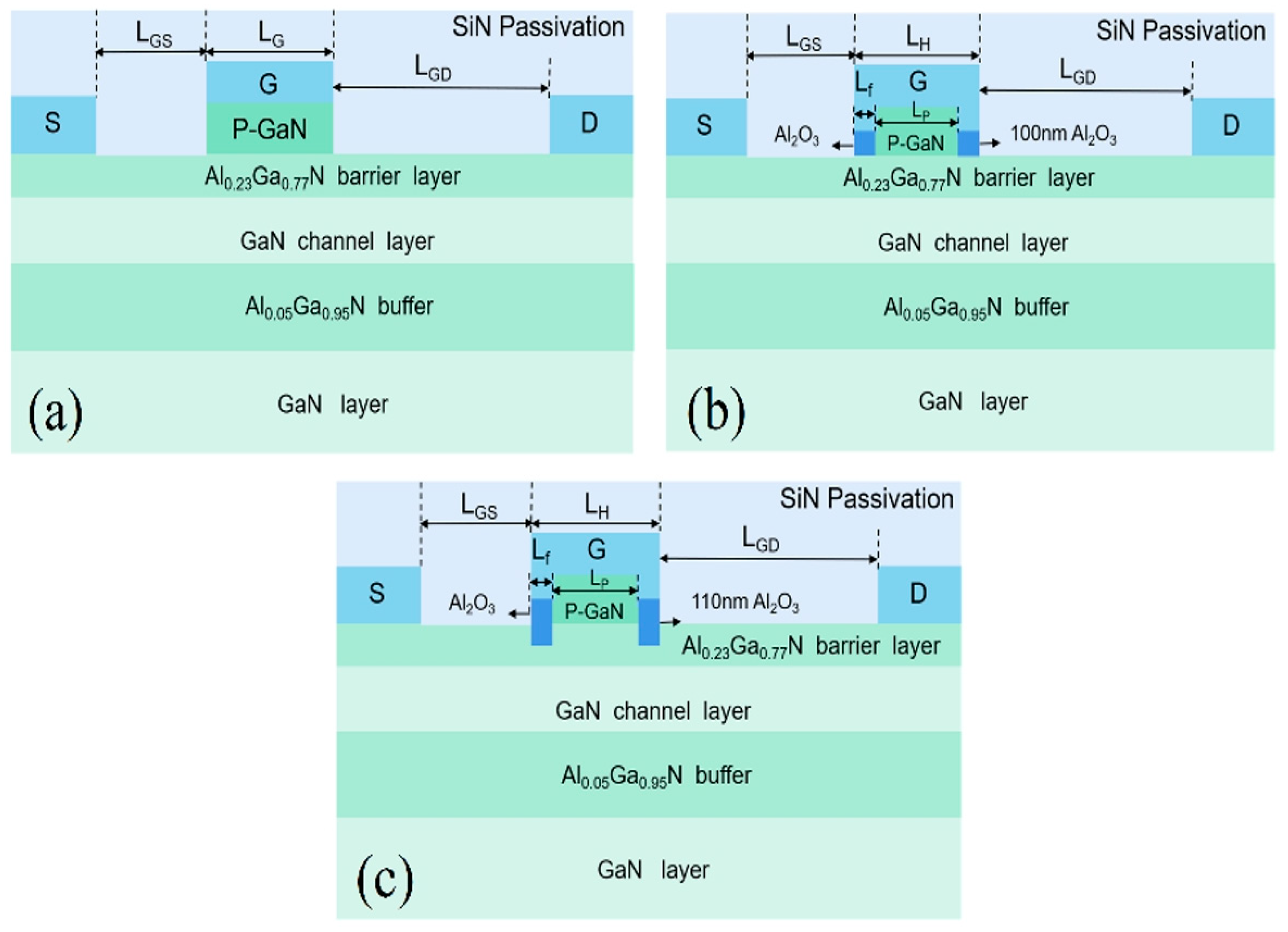
2. Device Structures and Simulation Parameters
3. Results and Discussion
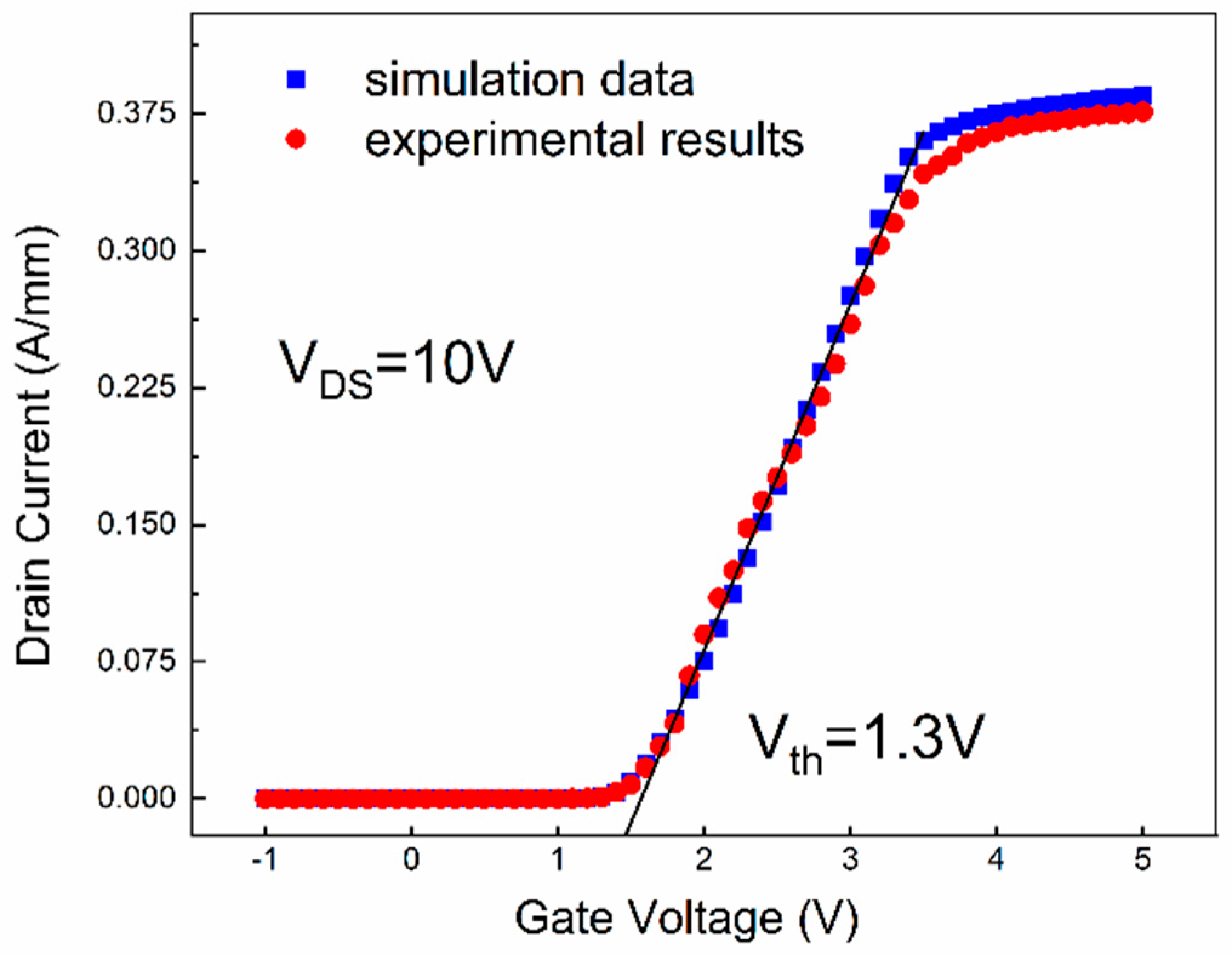
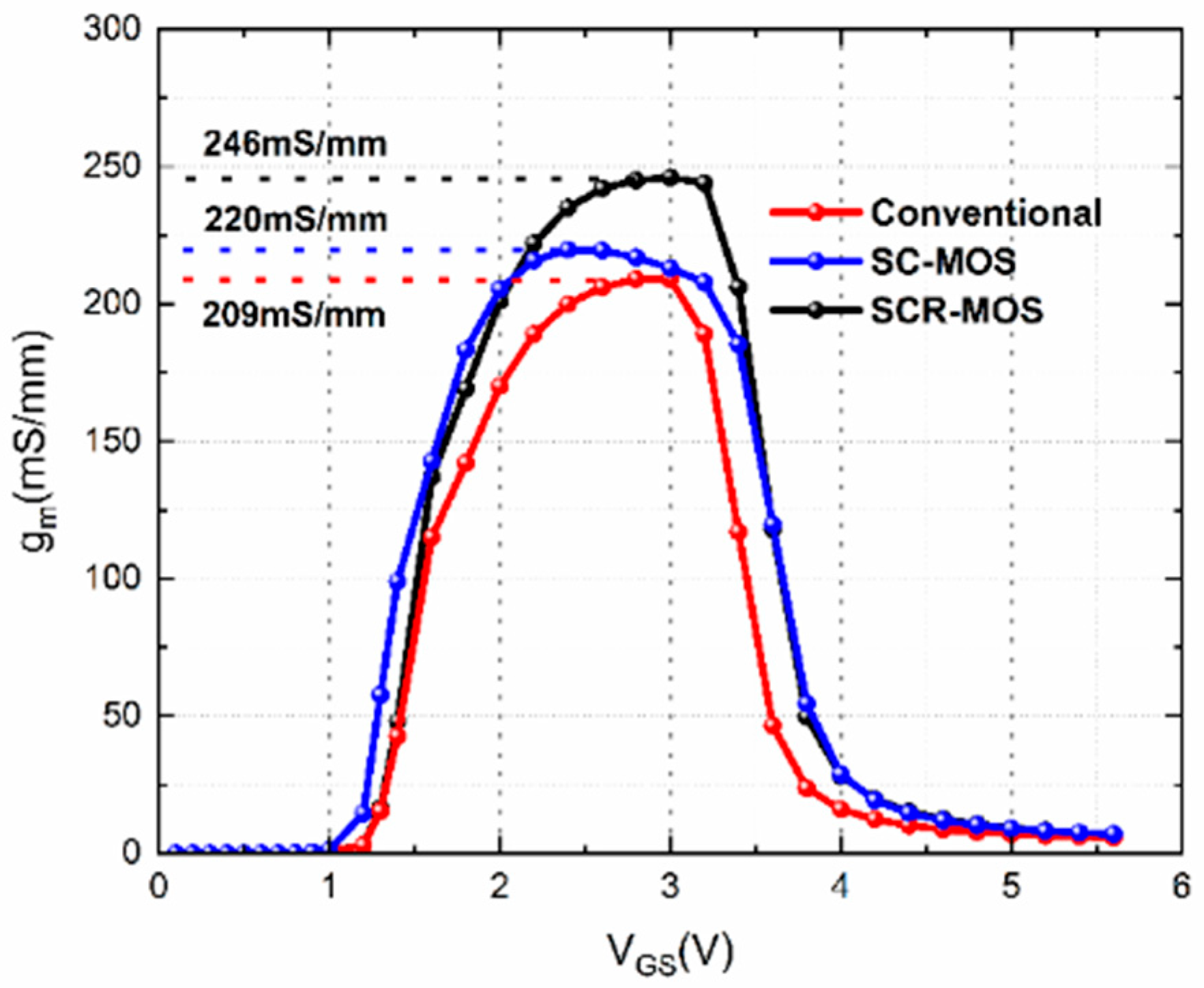
3.1. DC Performance
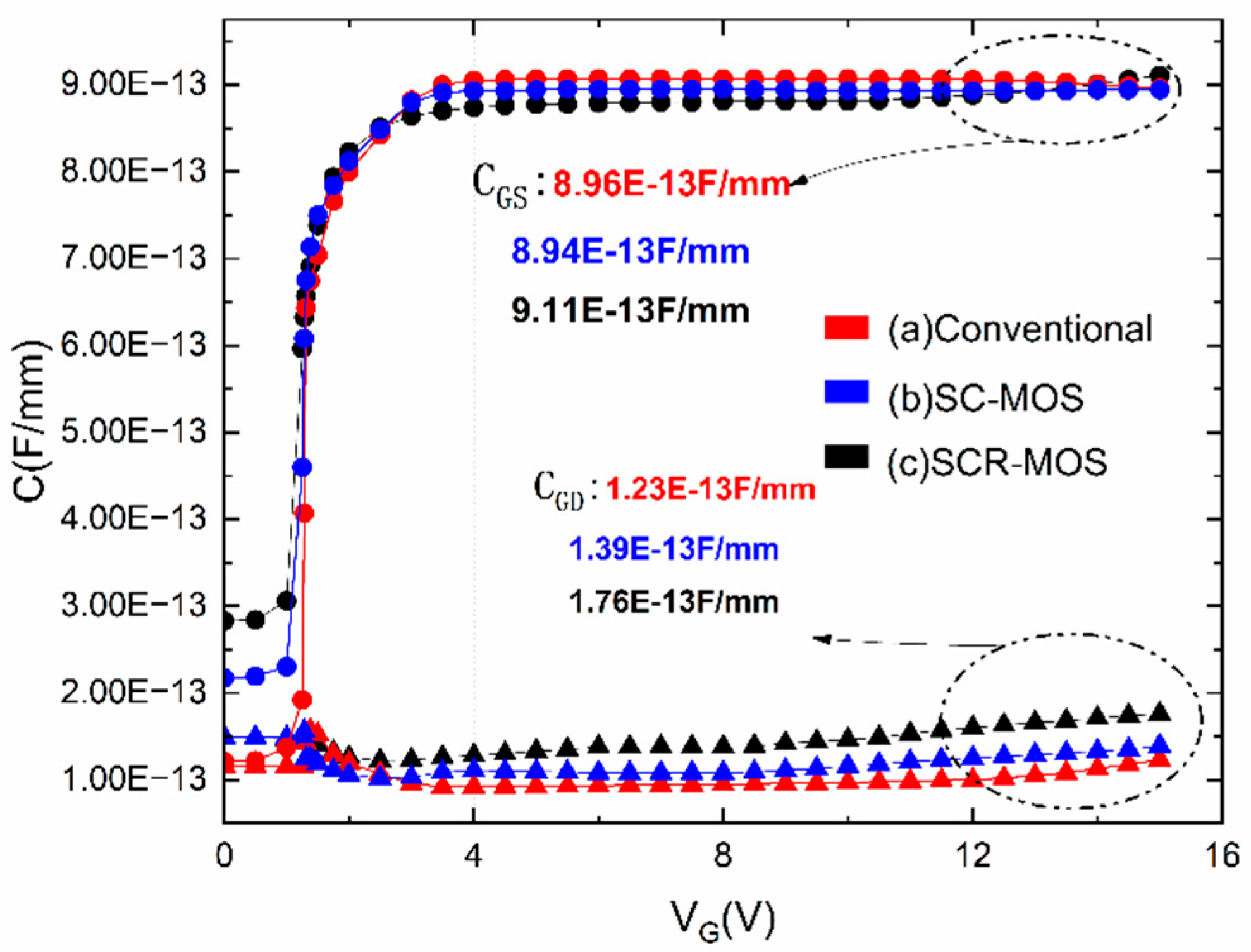
3.2. AC Performance
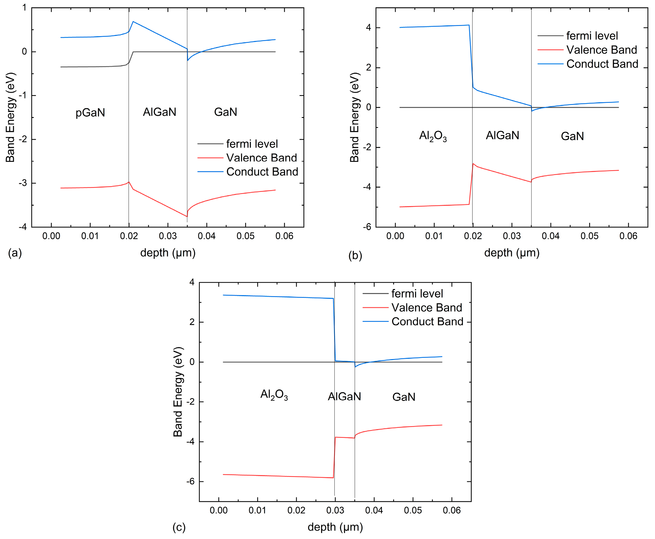
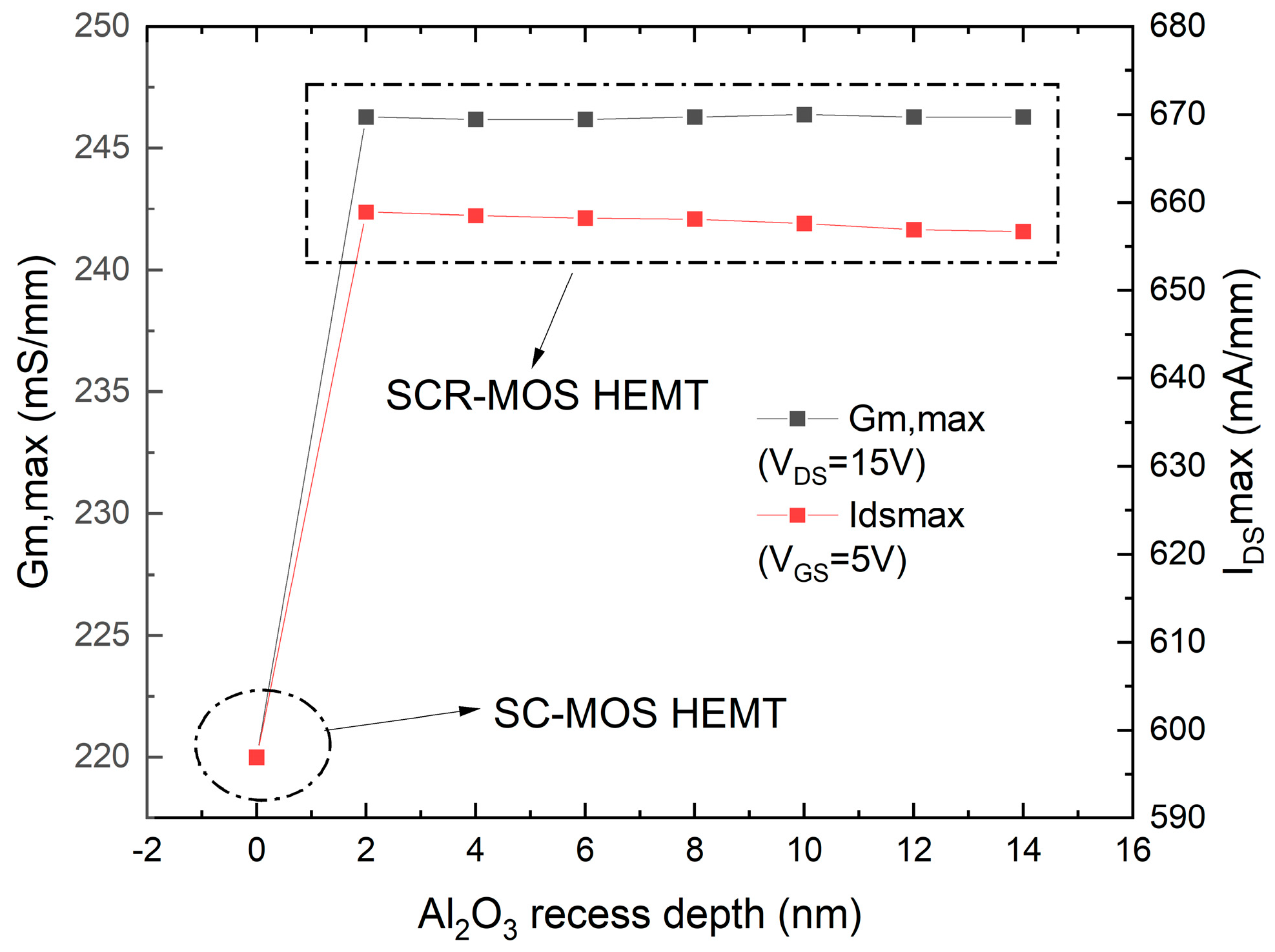
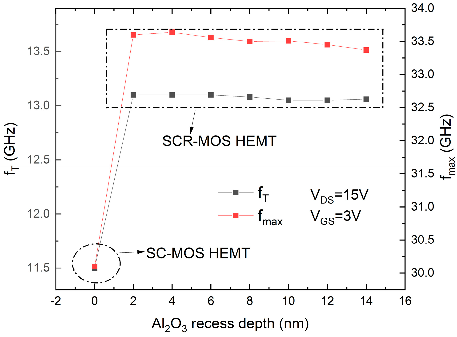
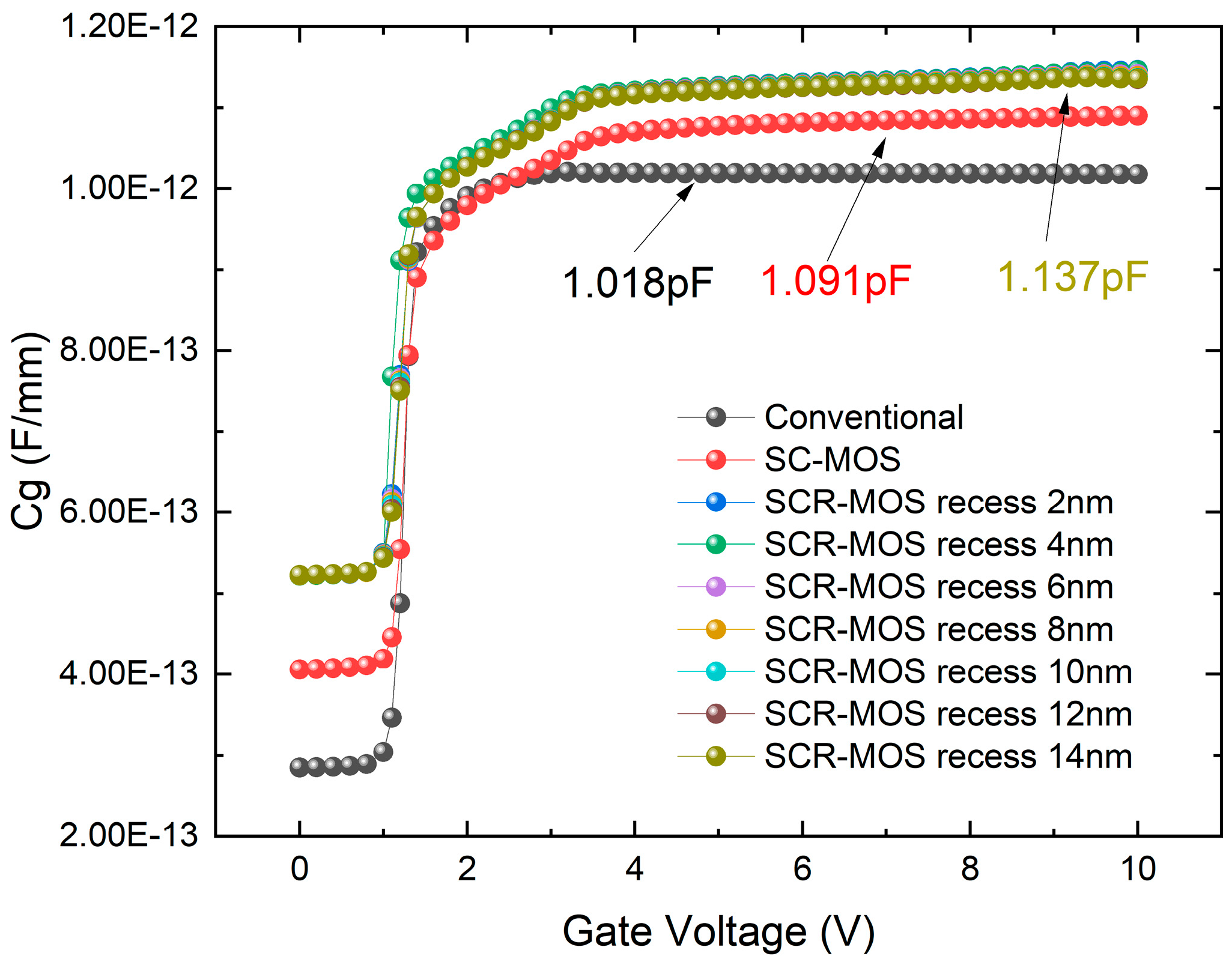
3.3. Physical Insight and Optimization
4. Conclusions
Author Contributions
Funding
Data Availability Statement
Conflicts of Interest
References
- Brinkhoff, J.; Parker, A.E. Characterising HEMT devices for MMIC distortion prediction. In Proceedings of the SPIE Conference Proceedings, Brisbane, Australia, 5 January 2006; Volume 6035, pp. 440–451. [Google Scholar] [CrossRef]
- Iucolano, F.; Boles, T. GaN-on-Si HEMTs for wireless base stations. Mater. Sci. Semicond. Process. 2019, 98, 100–105. [Google Scholar] [CrossRef]
- Lee, S.-Y.; Woo, J.; Park, S.; Kwon, Y. Linear X-band GaN HEMT transformer-based Doherty power amplifier. Electron. Lett. 2016, 52, 1342–1343. [Google Scholar] [CrossRef]
- Wu, T.-L.; Marcon, D.; You, S.; Posthuma, N.; Bakeroot, B. Forward Bias Gate Breakdown Mechanism in Enhancement-Mode p-GaN Gate AlGaN/GaN High-Electron Mobility Transistors. Electron Device Lett. 2015, 36, 1001–1003. [Google Scholar] [CrossRef]
- Wang, H.; Wei, J.; Xie, R.; Liu, C.; Tang, G.; Chen, K.J. Maximizing the Performance of 650-V p-GaN Gate HEMTs: Dynamic RON Characterization and Circuit Design Considerations. IEEE Trans. Power Electron. 2016, 32, 5539–5549. [Google Scholar] [CrossRef]
- Medjdoub, F.; Waldhoff, N.; Zegaoui, M.; Grimbert, B.; Rolland, N.; Rolland, P.A. Low-Noise Microwave Performance of AlN/GaN HEMTs Grown on Silicon Substrate. IEEE Electron Device Lett. 2011, 32, 1230–1232. [Google Scholar] [CrossRef]
- Allaei, M.; Shalchian, M.; Jazaeri, F. Modeling of short-channel effects in GaN HEMTs. IEEE Trans. Electron Devices 2020, 67, 3088–3094. [Google Scholar] [CrossRef]
- Saadaoui, S.; Fathallah, O.; Maaref, H. Effects of gate length on GaN HEMT performance at room temperature. J. Phys. Chem. Solids 2022, 161, 110418. [Google Scholar] [CrossRef]
- Moultif, N.; Latry, O.; Ndiaye, M.; Neveu, T.; Joubert, E.; Moreau, C.; Goupy, J.-F. S-band pulsed-RF operating life test on AlGaN/GaN HEMT devices for radar application. Microelectron. Reliab. 2019, 100–101, 113434. [Google Scholar] [CrossRef]
- Zanoni, E.; Santi, C.D.; Gao, Z.; Buffolo, M.; Fornasier, M.; Saro, M.; Pieri, F.D.; Rampazzo, F.; Meneghesso, G.; Meneghini, M.; et al. Microwave and millimeter-wave GaN HEMTs: Impact of epitaxial structure on short-channel effects, electron trapping, and reliability. IEEE Trans. Electron Devices 2024, 71, 1396–1407. [Google Scholar] [CrossRef]
- Guan, H.; Li, W.; Tong, X.; Shen, G.; Li, F.; Zhang, H. DC and RF performance of HR Si(111)-based AlGaN/GaN MIS-HEMT with a symmetrical multi-finger grid array structure for 5G N28 700MHz low-bias-control applications. Mater. Sci. Semicond. Process. 2023, 164, 107619. [Google Scholar] [CrossRef]
- Kim, J.-G. Optimization of epitaxial structures on GaN-on-Si (111) HEMTs with step-graded AlGaN buffer layer and AlGaN back barrier. Coatings 2024, 16, 700. [Google Scholar] [CrossRef]
- Dutta, G.; DasGupta, N.; DasGupta, A. Gate Leakage Mechanisms in AlInN/GaN and AlGaN/GaN MIS-HEMTs and Its Modeling. IEEE Trans. Electron Devices 2017, 64, 3609–3615. [Google Scholar] [CrossRef]
- Yagi, S.; Shimizu, M.; Inada, M.; Yamamoto, Y.; Piao, G.; Okumura, H.; Yano, Y.; Akutsu, N.; Ohashi, H. High breakdown voltage AlGaN/GaN MIS–HEMT with SiN and TiO2 gate insulator. Solid-State Electron. 2006, 50, 1057–1061. [Google Scholar] [CrossRef]
- Tang, Z.; Jiang, Q.; Lu, Y.; Huang, S.; Yang, S.; Tang, X. 600-V Normally Off SiNx/AlGaN/GaN MIS-HEMT With Large Gate Swing and Low Current Collapse. IEEE Electron Device Lett. 2013, 34, 1373–1375. [Google Scholar] [CrossRef]
- Liu, S.; Yang, S.; Tang, Z.; Jiang, Q.; Liu, C.; Wang, M.; Chen, K.J. Al2O3/AlN/GaN MOS-Channel-HEMTs With an AlN Interfacial Layer. IEEE Electron Device Lett. 2014, 35, 723–725. [Google Scholar] [CrossRef]
- Mondal, A.; Roy, A.; Mitra, R.; Kundu, A. Comparative Study of Variations in Gate Oxide Material of a Novel Underlap DG MOS-HEMT for Analog/RF and High Power Applications. Silicon 2020, 12, 2251–2257. [Google Scholar] [CrossRef]
- Chen, M.; Xu, J.; Cao, Y.; He, H.-Y.; Fan, K.N.; Zhuang, H. Dehydrogenation of propane over In2O3–Al2O3 mixed oxide in the presence of carbon dioxide. J. Catal. 2010, 272, 101–108. [Google Scholar] [CrossRef]
- Boryło, P.; Lukaszkowicz, K.; Szindler, M.; Kubacki, J.; Balin, K.; Basiaga, M.; Szewczenko, J. Structure and properties of Al2O3 thin films deposited by ALD process. Vacuum 2016, 131, 319–326. [Google Scholar] [CrossRef]
- Huang, S.; Liu, X.; Zhang, J.; Wei, K.; Liu, G.; Wang, X.; Zheng, Y.; Liu, H.; Jin, Z.; Zhao, C.; et al. High RF Performance Enhancement-Mode Al2O3/AlGaN/GaN MIS-HEMTs Fabricated with High-Temperature Gate-Recess Technique. IEEE Electron Device Lett. 2015, 36, 754–756. [Google Scholar] [CrossRef]
- Lee, C.-S.; Liao, Y.-H.; Chou, B.-Y.; Liu, H.-Y.; Hsu, W.-C. Composite HfO2/Al2O3-dielectric AlGaAs/InGaAs MOS-HEMTs by using RF sputtering/ozone water oxidation. Superlattices Microstruct. 2014, 72, 194–203. [Google Scholar] [CrossRef]
- Hilt, O.; Knauer, A.; Brunner, F.; Treidel, E.B.; Würfl, J. Normally-off AlGaN/GaN HFET with p-type GaN gate and AlGaN buffer. In Proceedings of the 6th International Conference on Integrated Power Electronics Systems, Nuremberg, Germany, 16–18 March 2010. [Google Scholar]
- Treidel, E.B.; Hilt, O.; Brunner, F.; Sidorov, V.; Würfl, J.; Tränkle, G. AlGaN/GaN/AlGaN DH-HEMTs Breakdown Voltage Enhancement Using Multiple Grating Field Plates (MGFPs). IEEE Trans. Electron Devices 2010, 57, 1206–1208. [Google Scholar] [CrossRef]
- Oğuzman, I.H.; Bellotti, E.; Brennan, K.F.; Kolník, J.; Wang, R.; Ruden, P.P. Theory of hole initiated impact ionization in bulk zincblende and wurtzite GaN. J. Appl. Phys. 1997, 81, 7827–7834. [Google Scholar] [CrossRef]
- Mnatsakanov, T.T.; Levinshtein, M.E.; Pomortseva, L.I.; Yurkov, S.N.; Simin, G.S.; Khan, M.A. Carrier mobility model for GaN. Solid-State Electron. 2003, 47, 111–115. [Google Scholar] [CrossRef]
- Gryglewski, D.; Wojtasiak, W.; Kamińska, E.; Piotrowska, A. Characterization of Self-Heating Process in GaN-Based HEMTs. Electronics 2020, 9, 1305. [Google Scholar] [CrossRef]


| Symbol | Statement | Value |
|---|---|---|
| LGS | Gate–source distance | 1.1 μm |
| LGD | Gate–drain distance | 6 μm |
| LG&LH | Length of gate and length of p-GaN in traditional HEMT | 1.4 μm |
| LP | Length of p-GaN in SC-MOS HEMT and SCR-MOS HEMT | 1 μm |
| Lf | Length of gate foot | 0.2 μm |
| TP | Thickness of p-GaN | 110 nm |
| Tb | Thickness of AlGaN barrier | 15 nm |
| Ho | Height of oxide above barrier layer | 100 nm |
| Do | Depth of oxide recessed in barrier layer | 10 nm |
| Parameter | Symbol | Value |
|---|---|---|
| Lattice constant | a0 | 3.189 Å |
| Elastic constant | C33 | 392 Gpa |
| Elastic constant | C13 | 100 Gpa |
| Spontaneous polarization | Psp | −0.034 C·m−2 |
| Piezoelectric const.(z) | E33 | 0.68 C·m−2 |
| Piezoelectric const.(x,y) | E31 | −0.32 C·m−2 |
Disclaimer/Publisher’s Note: The statements, opinions and data contained in all publications are solely those of the individual author(s) and contributor(s) and not of MDPI and/or the editor(s). MDPI and/or the editor(s) disclaim responsibility for any injury to people or property resulting from any ideas, methods, instructions or products referred to in the content. |
© 2025 by the authors. Licensee MDPI, Basel, Switzerland. This article is an open access article distributed under the terms and conditions of the Creative Commons Attribution (CC BY) license (https://creativecommons.org/licenses/by/4.0/).
Share and Cite
Li, Y.; Huang, Y.; Li, J.; Sun, H.; Guo, Z. Effect of Dual Al2O3 MIS Gate Structure on DC and RF Characteristics of Enhancement-Mode GaN HEMT. Micromachines 2025, 16, 687. https://doi.org/10.3390/mi16060687
Li Y, Huang Y, Li J, Sun H, Guo Z. Effect of Dual Al2O3 MIS Gate Structure on DC and RF Characteristics of Enhancement-Mode GaN HEMT. Micromachines. 2025; 16(6):687. https://doi.org/10.3390/mi16060687
Chicago/Turabian StyleLi, Yuan, Yong Huang, Jing Li, Huiqing Sun, and Zhiyou Guo. 2025. "Effect of Dual Al2O3 MIS Gate Structure on DC and RF Characteristics of Enhancement-Mode GaN HEMT" Micromachines 16, no. 6: 687. https://doi.org/10.3390/mi16060687
APA StyleLi, Y., Huang, Y., Li, J., Sun, H., & Guo, Z. (2025). Effect of Dual Al2O3 MIS Gate Structure on DC and RF Characteristics of Enhancement-Mode GaN HEMT. Micromachines, 16(6), 687. https://doi.org/10.3390/mi16060687