Investigation of Channel Mobility Enhancement Techniques Using Si/SiGe/GeSn Materials in Orthogonally Oriented Selective Buried Triple Gate Vertical Power MOSFET: Design and Performance Analysis
Abstract
1. Introduction
2. Device Structure, Performance, and Process Flow
3. Si(1−x)Gex Triple Gate MOSFET
4. Ge(1−x)Snx Triple Gate MOSFET
4.1. Performance of GeSn Triple Gate Power MOSFET with Other Channel Material
4.2. Device Sensitivity, Mobility, and Gate Charge Analysis
5. Conclusions
Author Contributions
Funding
Data Availability Statement
Acknowledgments
Conflicts of Interest
References
- Baliga, B. Fundamentals of Power Semiconductor Devices; Springer: New York, NY, USA, 2008. [Google Scholar]
- Adler, M.S.; Owyang, K.W.; Baliga, B.J.; Kokosa, R.A. The evolution of power device technology. IEEE Trans. Electron Devices 1984, 31, 1570–1591. [Google Scholar] [CrossRef]
- Grant, D. Power semiconductor devices—Continuous development. Microelctronics J. 1996, 27, 161–176. [Google Scholar] [CrossRef]
- Zhu, M.; Ma, J.; Nela, L.; Matioli, E. High-performance normally-off tri-gate GaN power MOSFETs. In Proceedings of the 31st International Symposium on Power Semiconductor Devices & ICs, Shanghai, China, 19–23 May 2019. [Google Scholar]
- Cooper, J.; Islam, N. Vertical Tri-Gate Power MOSFETs 4H-SiC. Mater. Sci. Forum 2018, 924, 680–683. [Google Scholar] [CrossRef]
- Tega, N.; Yoshimoto, H.; Hisamoto, D.; Watanabe, N.; Shimizu, H.; Sato, S.; Mori, Y.; Ishigaki, T.; Matsumura, M.; Konishi, K.; et al. Novel trench-etched double-diffused SiC MOS (TED MOS) for overcoming tradeoff between RonA and Qgd. In Proceedings of the IEEE 27th International Symposium on Power Semiconductor Devices & IC’s (ISPSD), Hong Kong, China, 10–14 May 2015; pp. 81–84. [Google Scholar] [CrossRef]
- Ramamurthy, R.P.; Islam, N.; Sampath, M.; Morisette, D.T.; Cooper, J.A. The Tri-Gate MOSFET: A New Vertical Power Transistor in 4H-SiC. IEEE Electron Device Lett. 2021, 42, 90–93. [Google Scholar] [CrossRef]
- Juang, M.H.; Chueh, W.C.; Jang, S.L. The formation of trench-gate power MOSFETs with a SiGe channel region. Semicond. Sci. Technol. 2006, 21, 799–802. [Google Scholar] [CrossRef]
- Schulte-Braucks, C.; Glass, S.; Hofmann, E.; Stange, D.; von den Driesch, N.; Hartmann, J.M.; Ikonic, Z.; Zhao, Q.T.; Buca, D.; Mantl, S. Process modules for GeSn nanoelectronics with high Sn-contents. Solid-State Electron. 2017, 128, 54–59. [Google Scholar] [CrossRef]
- Silvaco. ATLAS User’s Manual: Device Simulation Software; Version 4.2.0.R.; Silvaco: Santa Clara, CA, USA, 2015. [Google Scholar]
- Wang, Y.; Liu, Y.J.; Yu, C.H.; Cao, F. A Novel Trench-Gated Power MOSFET with Reduced Gate Charge. IEEE Electron Device Lett. 2014, 36, 165–167. [Google Scholar] [CrossRef]
- Nigar, H.; Loan, S.A. Impact of Gate-Drift Overlap on the Figure of Merits of Dual Buried Gates Power MOSFET. In Proceedings of the International Conference on Electrical, Electronics and Computer Engineering (UPCON), Aligarh, India, 8–10 November 2019. [Google Scholar] [CrossRef]
- Von der Meulen, Y.J. Kinetics of Thermal Growth of Ultra-Thin Layers of SiO2 on Silicon I. Experiment. J. Electrochem. Soc. 1972, 119, 530–534. [Google Scholar] [CrossRef]
- Faraone, L. Thermal SiO2 films on n+ poly crystalline silicon: Electrical conduction and breakdown. IEEE Trans. Electron Devices 1986, 33, 1785–1794. [Google Scholar] [CrossRef]
- Chen, L.; Wu, Y.; Chiang, J.; Hung, M.; Chang, C.; Su, P. Comprehensive Study of Pi-Gate Nanowires poly-Si TFT Nonvolatile Memory with an HfO2 Charge Trapping Layer. IEEE Trans. Nanotechnol. 2011, 10, 260–265. [Google Scholar] [CrossRef]
- Goarin, P.; Koops, G.E.J.; Van Dalen, R.; Le Cam, C.; Saby, J. Split-gate Resurf Stepped Oxide (RSO) MOSFETs for 25V applications with record low gate-to-drain charge. In Proceedings of the 19th International Symposium on Power Semiconductor Devices and IC’s, Jeju Island, Republic of Korea, 27–31 May 2007; pp. 61–64. [Google Scholar] [CrossRef]
- Kim, J.; Roh, T.M.; Kim, S.G.; Park, I.Y.; Yang, Y.S.; Lee, D.W.; Koo, J.G.; Cho, K.I.; Kang, Y.I. A Novel Process for Fabricating High Density Trench MOSFETs for DC-DC Converters. ETRI J. 2002, 24, 333–340. [Google Scholar] [CrossRef]
- Denton, J.P.; Neudeck, G.W. Fully depleted dual-gated thin-film SOI P-MOSFETs fabricated in SOI islands with an isolated buried poly silicon backgate. IEEE Electron Device Lett. 1996, 17, 509–511. [Google Scholar] [CrossRef]
- Calafut, D.S. Power Mos Device with Improved Gate Charge Performance. U.S. Patent 6,461,918 B1, 8 October 2002. [Google Scholar]
- Wang, Y.; Hu, H.; Jiao, W.; Cheng, C. Gate Enhanced Power UMOSFET with Ultralow On-Resistance. IEEE Electron Device Lett. 2010, 31, 338–340. [Google Scholar] [CrossRef]
- Jiang, Q.; Wang, M.; Chen, X. A High-Speed Deep-Trench MOSFET with a Self-Biased Split Gate. IEEE Trans. Electron Devices 2010, 57, 1972–1977. [Google Scholar] [CrossRef]
- Wirths, S.; Buca, D.; Tiedemann, A.T.; Holländer, B.; Bernardy, P.; Stoica, T.; Grützmacher, D.; Mantl, S. Epitaxial growth of Ge1–xSnx by reduced pressure CVD using SnCl4 and Ge2H6. ECS Trans. 2013, 50, 885–893. [Google Scholar] [CrossRef]
- Singh, Y.; Punetha, M. A Lateral Trench Dual Gate Power MOSFET on Thin SOI for Improved Performance. ECS J. Solid State Sci. Technol. 2013, 2, Q113–Q117. [Google Scholar] [CrossRef]
- Erlbacher, T.; Bauer, A.J.; Frey, L. Reduced on Resistance in LDMOS Devices by Integrating Trench Gates into Planar Technology. IEEE Electron Device Lett. 2010, 31, 464–466. [Google Scholar] [CrossRef]
- Na, K.I.; Kim, S.G.; Koo, J.G.; Kim, J.D.; Yang, Y.S.; Lee, J.H. Simulation and Fabrication Studies of Semi-superjunction Trench Power MOSFETs by RSO Process with Silicon Nitride Layer. ETRI J. 2012, 34, 962–965. [Google Scholar] [CrossRef]
- Ng, J.C.W. A New Trench Power MOSFET With an Inverted L-Shaped Source Region. IEEE Electron Device Lett. 2010, 31, 1284–1286. [Google Scholar] [CrossRef]
- Nigar, H.; Alkhammash, H.I.; Qamar, S.; Loan, S.A. A Uni-gate vertical power MOSFET with improved figure of Merits: Design and analysis. Alex. Eng. J. 2023, 67, 31–38. [Google Scholar] [CrossRef]
- Nigar, H.; Loan, S.A. High performance selective buried double gate power MOSFET. Semicond. Sci. Technol. 2019, 34, 05LT01. [Google Scholar] [CrossRef]
- Wei, Y.; Luo, X.; Ge, W.; Zhao, Z.; Ma, Z.; Wei, J. A Split Triple-Gate Power LDMOS with Improved Static-State and Switching Performance. IEEE Trans. Electron Devices 2019, 66, 2669–2674. [Google Scholar] [CrossRef]
- He, J.; Hua, M.; Zhang, Z.; Chen, K. Performance and VTH Stability in E-Mode GaN Fully Recessed MIS-FETs and Partially Recessed MIS-HEMTs with LPCVD-SiNx/PECVD-SiNx Gate Dielectric Stack. IEEE Trans. Electron Devices 2018, 65, 3185–3191. [Google Scholar] [CrossRef]
- Matioli, E.; Palacios, T. Tri-Gate Normally-Off GaN Power MISFET. IEEE Electron Device Lett. 2012, 33, 360–362. [Google Scholar]
- Jagadesh, M.; Sithanandam, R. Extended-p+ Stepped Gate LDMOS for Improved Performance. IEEE Trans. Electron Devices 2010, 57, 1719–1724. [Google Scholar]
- Naguma, T.; Hiramoto, T. Design Guideline of Multi-Gate MOSFETs with Substrate-Bias Control. IEEE Trans. Electron Devices 2006, 53, 3025–3031. [Google Scholar] [CrossRef]
- Zhu, M.; Ma, J.; Nela, L.; Erine, C.; Matioli, E. High-voltage normally-off recessed tri-gate GaN power MOSFETs with low on-resistance. IEEE Electron Device Lett. 2019, 40, 1289–1292. [Google Scholar] [CrossRef]
- Chiang, M.-H.; Lin, J.-N.; Kim, K.; Chuang, C.-T. Optimal Design of Triple-Gate Devices for High-Performance and Low-Power Applications. IEEE Trans. Electron Devices 2008, 55, 2423–2428. [Google Scholar] [CrossRef]
- Gunawan, O.; Sekaric, L.; Majumdar, A.; Rooks, M.; Appenzeller, J.; Sleight, J.W.; Guha, S.; Haensch, W. Measurement of Carrier Mobility in Silicon Nanowires. Nano Lett. 2008, 8, 1566–1571. [Google Scholar] [CrossRef]
- An, S.; Park, H.; Kim, M. Recent advances in single crystal narrow bandgap semiconductor nanomembranes and their flexible optoelectronic device applications: Ge, GeSn, InGaAs, and 2D materials. J. Mater. Chem. C 2023, 11, 2430–2448. [Google Scholar] [CrossRef]
- Chuang, Y.; Liu, C.Y.; Luo, G.L.; Li, J.Y. Electron mobility enhancement in GeSn n-channel MOSFETs by tensile strain. IEEE Electron Device Lett. 2020, 42, 10–13. [Google Scholar] [CrossRef]
- Liu, T.-H.; Chiu, P.Y.; Chuang, Y.; Liu, C.Y.; Shen, C.H.; Luo, G.L.; Li, J.Y. High-mobility GeSn n-channel MOSFETs by low temperature chemical vapor deposition and microwave annealing. IEEE Electron Device Lett. 2018, 39, 468–471. [Google Scholar] [CrossRef]
- Gupta, S.; Vincent, B.; Yang, B.; Lin, D.; Gencarelli, F.; Lin, J.Y.; Chen, R.; Richard, O.; Bender, H.; Magyari-Köpe, B.; et al. Towards high mobility GeSn channel nMOSFETs: Improved surface passivation using novel ozone oxidation method. In Proceedings of the 2012 International Electron Devices Meeting, San Francisco, CA, USA, 10–13 December 2012. [Google Scholar]
- Mizuno, T.; Takagi, S.; Sugiyama, N.; Satake, H.; Kurobe, A.; Toriumi, A. Electron and hole mobility enhancement in strained-Si MOSFET’s on SiGe-on-insulator substrates fabricated by SIMOX technology. IEEE Electron Device Lett. 2000, 21, 230. [Google Scholar] [CrossRef]
- Welser, J.; Hoyt, J.L.; Gibbons, J.F. Electron Mobility Enhancement in Strained-Si N-Type Metal-Oxide-Semiconductor Field-Effect Transistors. IEEE Electron Device Lett. 1994, 15, 100–102. [Google Scholar] [CrossRef]
- Wu, Y.H.; Kim, H.H.; Shin, J.C. Improved mobility in InAs nanowire FETs with sulfur-based surface treatment. Curr. Appl. Phys. 2025, 70, 81–86. [Google Scholar] [CrossRef]
- Gnani, E.; Gnudi, A.; Reggiani, S.; Baccarani, G. An investigation on Effective Mobility in Nanowire FETs under Quasi-Ballistic Conditions. IEEE Trans. Electron Devices 2010, 57, 336–344. [Google Scholar] [CrossRef]
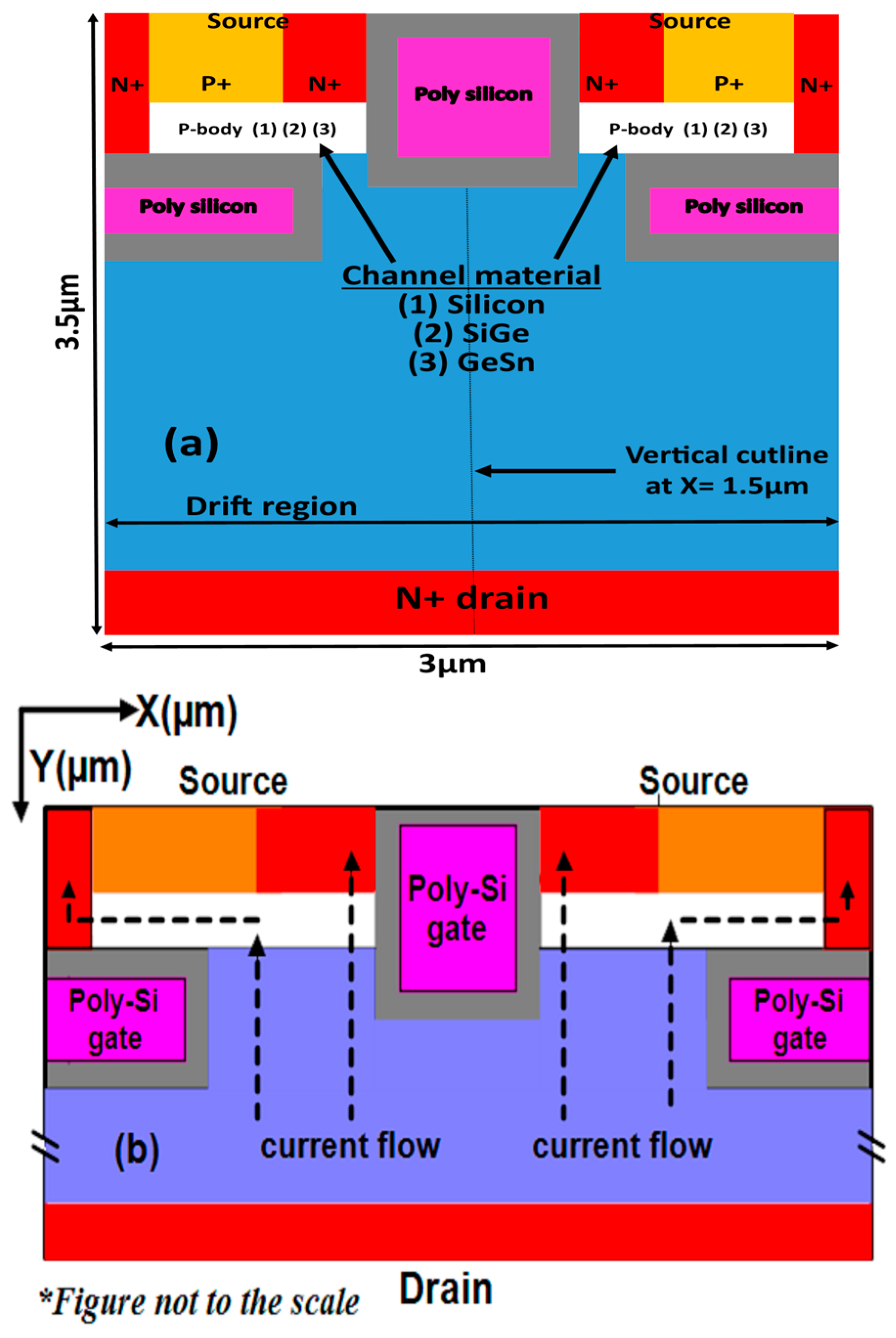
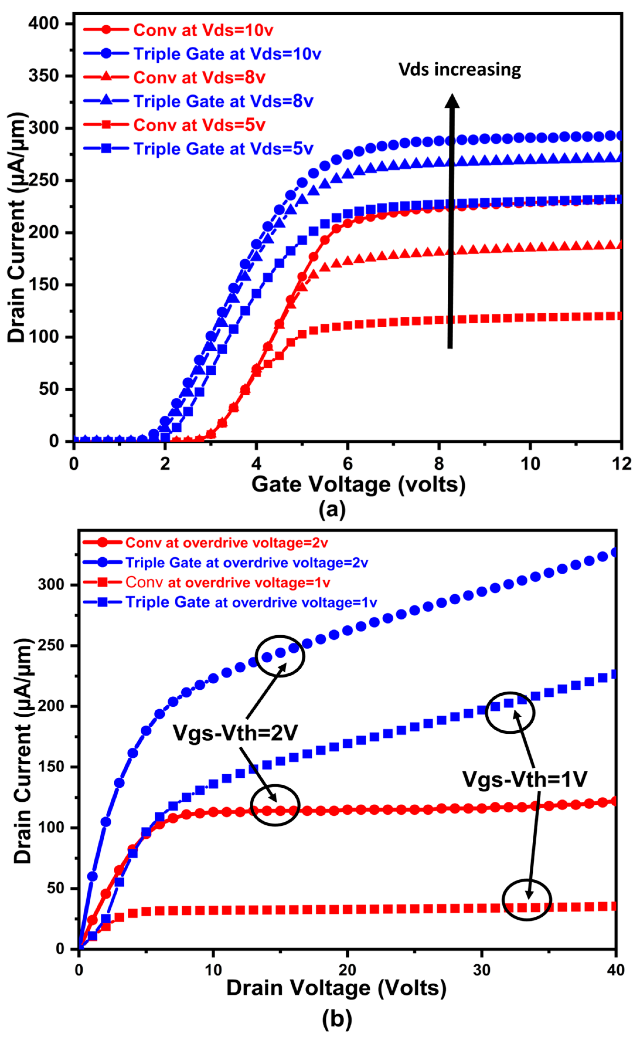
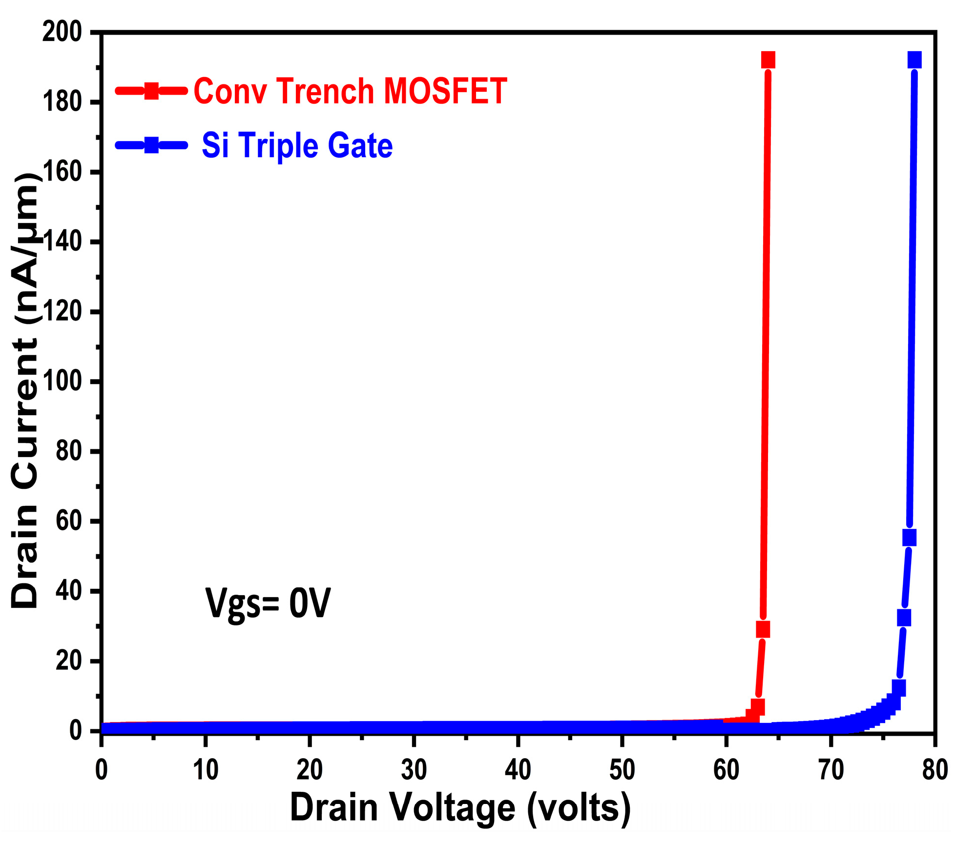

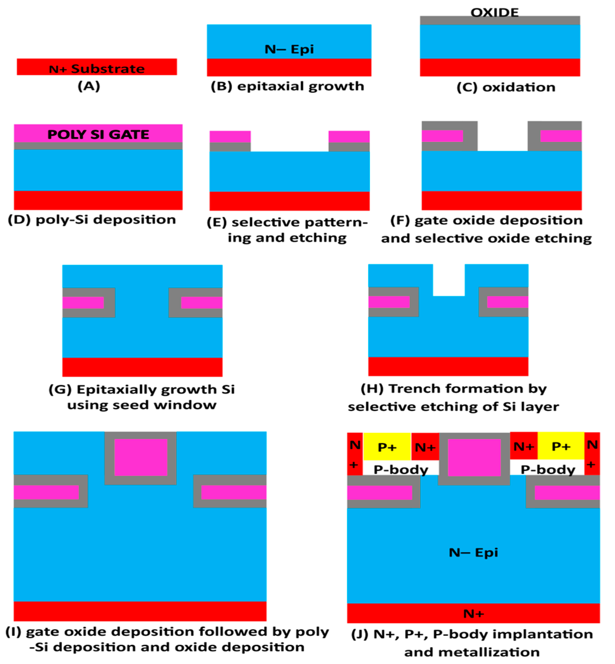
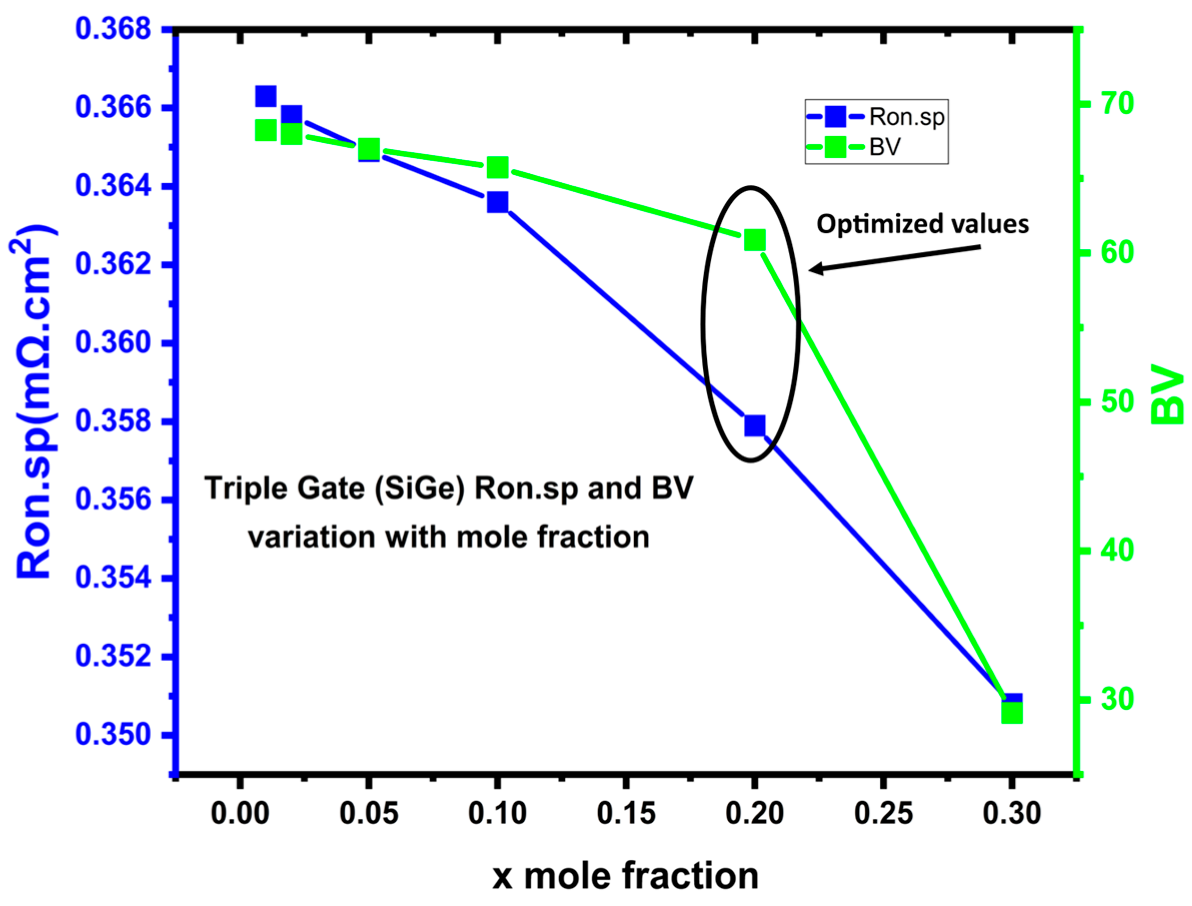
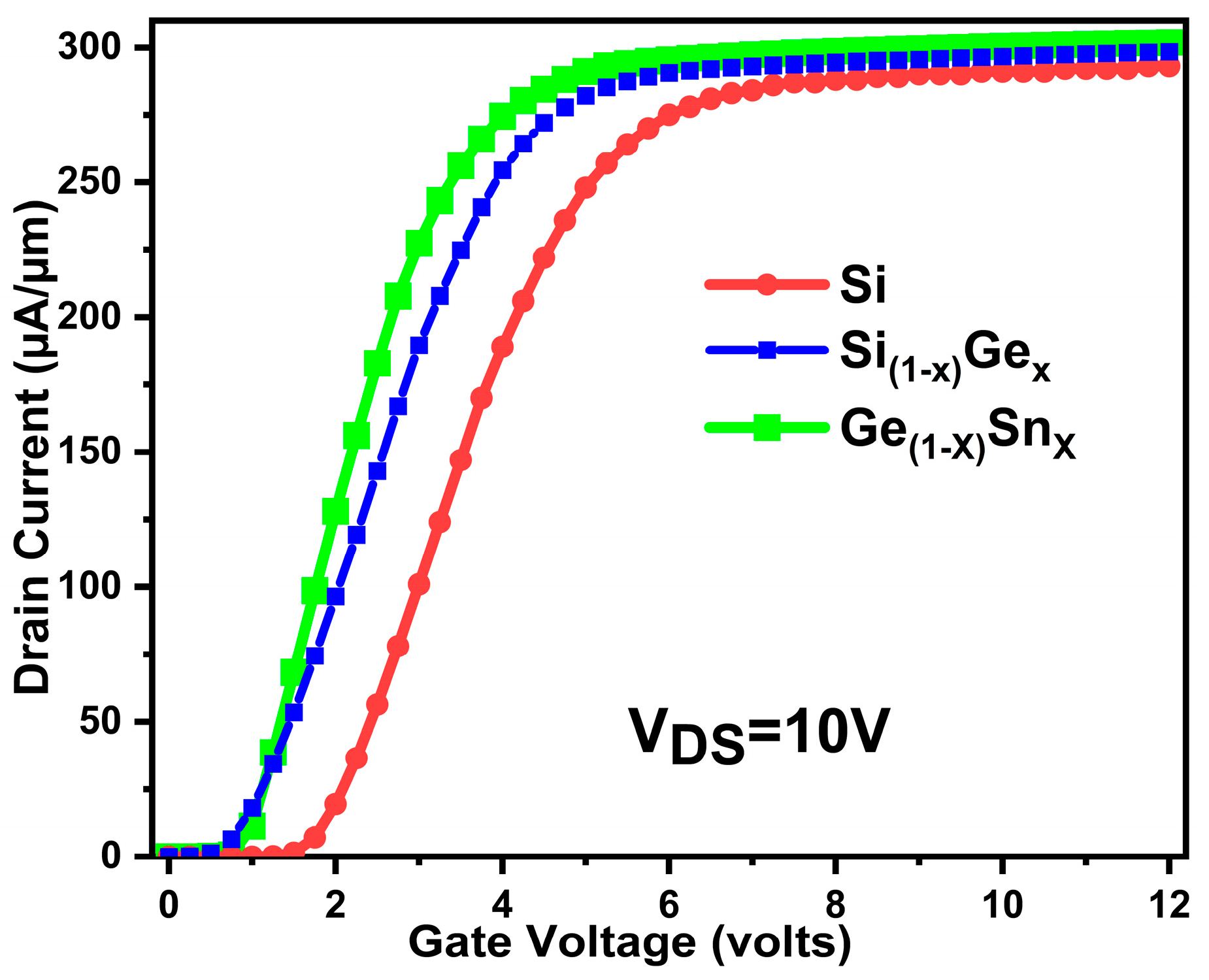

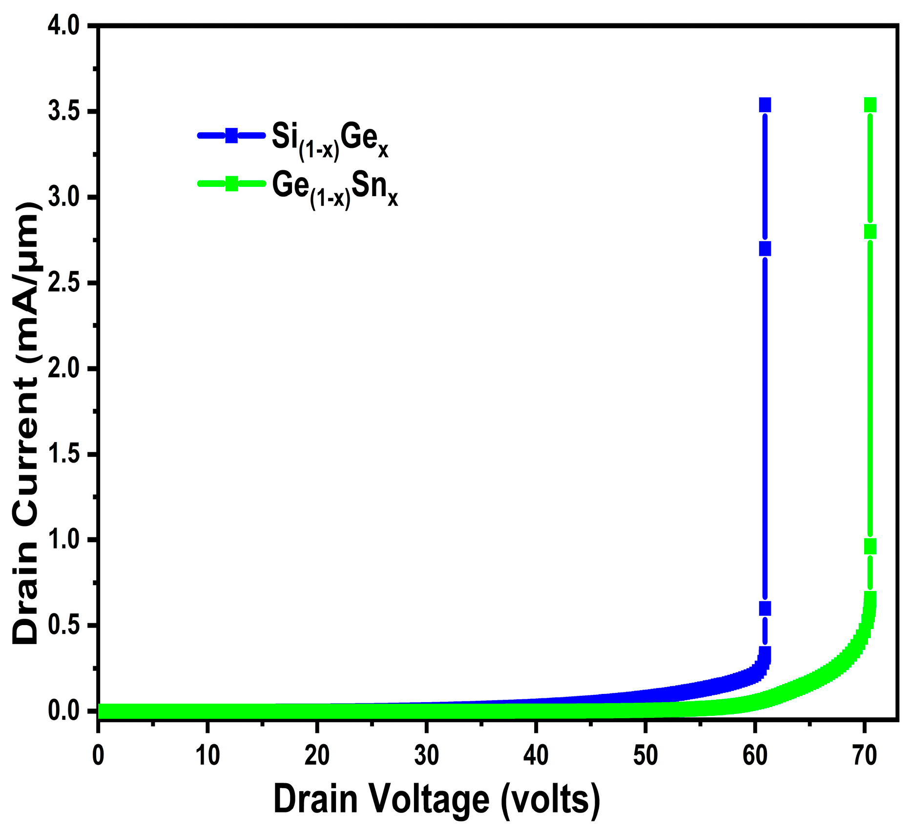
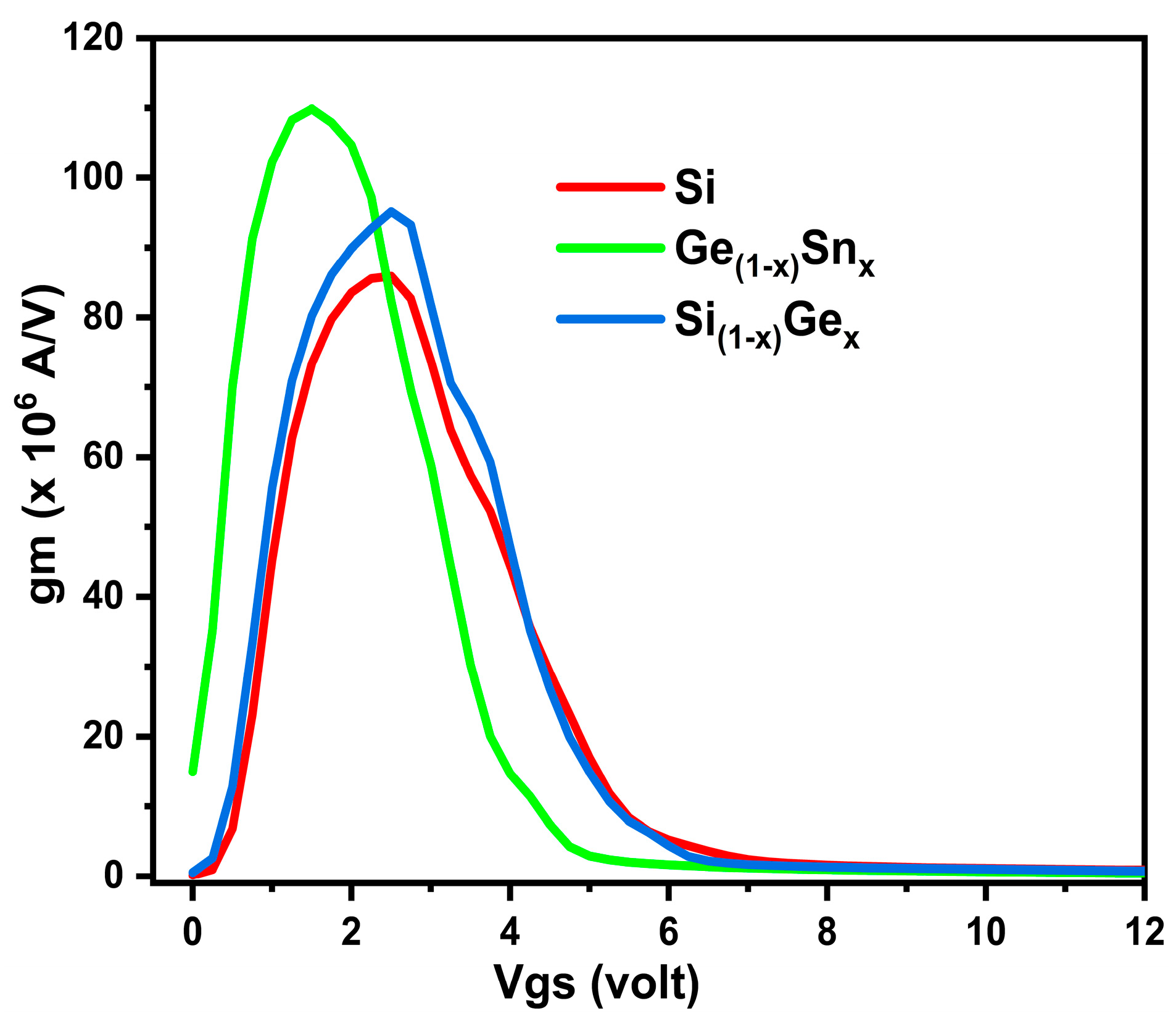
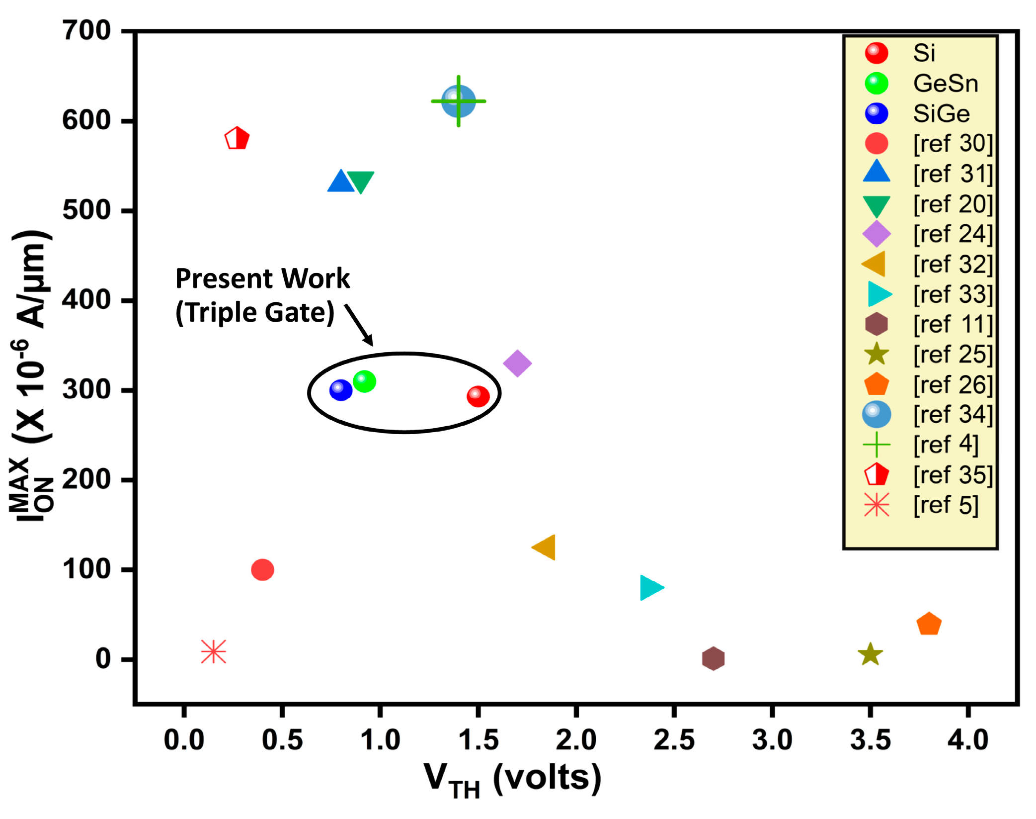
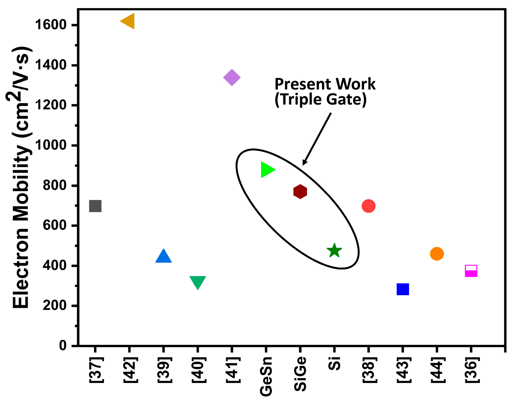
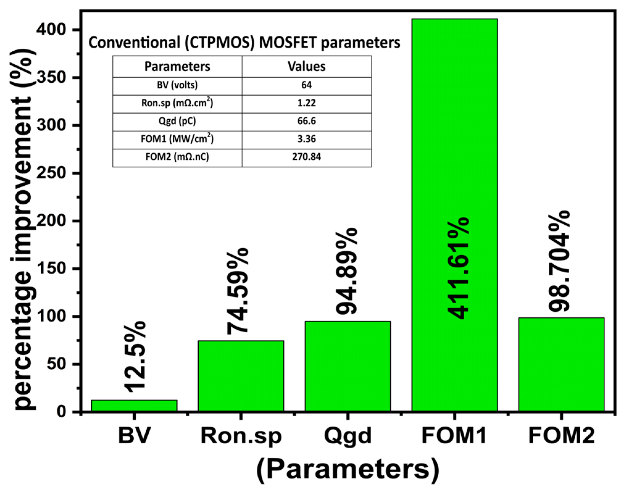
| Parameters | Conventional Trench Power MOSFET [11] | Proposed Vertical Triple Gate Device |
|---|---|---|
| Cell pitch | 3 µm | 3 µm |
| Trench width | 1 µm | Lateral gate = 0.65 µm (each), Vertical gate = 1 µm |
| Trench depth | 1.3 µm | Lateral gate = 0.1 µm (each), Vertical gate = 0.45 µm |
| Gate oxide thickness | 50 nm | 50 nm |
| N+ source width along vertical trench | ---- | 0.334 µm |
| Source doping | 1 × 10¹⁹/cm3 | 1 × 10¹⁹/cm3 |
| Source depth | 0.2 µm | 0.5 µm |
| N-drift region doping | 5.6 × 10¹⁴/cm3 | 5 × 10¹⁵/cm3 |
| p-body doping | 1.7 × 10¹⁷/cm3 | 1.2 × 10¹⁷/cm3 |
| P+ doping | 2 × 10¹⁹/cm3 | 2 × 10¹⁹/cm3 |
| N+ drain doping | 1 × 10¹⁹/cm3 | 1 × 10¹⁹/cm3 |
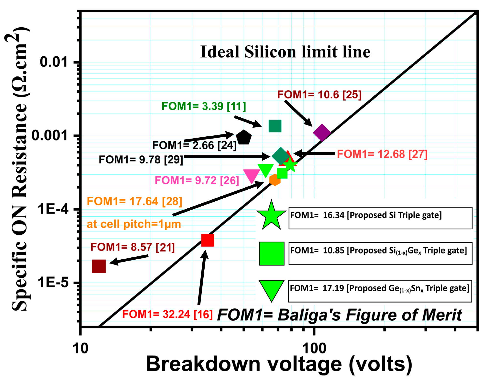
| Figure of Merit (FOM) | Proposed Triple Gate (Si Channel) | Proposed Triple Gate (SiGe Channel) | Proposed Triple Gate (GeSn Channel) |
|---|---|---|---|
| FOM1 (BV2/Ron) | 16.34 (MW/cm2) | 10.85 (MW/cm2) | 17.19 (MW/cm2) |
| FOM2 (Ron. Qgd) | 4.5 (mΩ·nC) | 4.08 (mΩ·nC) | 3.51 (mΩ·nC) |
Disclaimer/Publisher’s Note: The statements, opinions and data contained in all publications are solely those of the individual author(s) and contributor(s) and not of MDPI and/or the editor(s). MDPI and/or the editor(s) disclaim responsibility for any injury to people or property resulting from any ideas, methods, instructions or products referred to in the content. |
© 2025 by the authors. Licensee MDPI, Basel, Switzerland. This article is an open access article distributed under the terms and conditions of the Creative Commons Attribution (CC BY) license (https://creativecommons.org/licenses/by/4.0/).
Share and Cite
Lodhi, M.E.A.; Ansari, A.Q.; Loan, S.A.; Urooj, S.; Nasser, N. Investigation of Channel Mobility Enhancement Techniques Using Si/SiGe/GeSn Materials in Orthogonally Oriented Selective Buried Triple Gate Vertical Power MOSFET: Design and Performance Analysis. Micromachines 2025, 16, 452. https://doi.org/10.3390/mi16040452
Lodhi MEA, Ansari AQ, Loan SA, Urooj S, Nasser N. Investigation of Channel Mobility Enhancement Techniques Using Si/SiGe/GeSn Materials in Orthogonally Oriented Selective Buried Triple Gate Vertical Power MOSFET: Design and Performance Analysis. Micromachines. 2025; 16(4):452. https://doi.org/10.3390/mi16040452
Chicago/Turabian StyleLodhi, M. Ejaz Aslam, Abdul Quaiyum Ansari, Sajad A. Loan, Shabana Urooj, and Nidal Nasser. 2025. "Investigation of Channel Mobility Enhancement Techniques Using Si/SiGe/GeSn Materials in Orthogonally Oriented Selective Buried Triple Gate Vertical Power MOSFET: Design and Performance Analysis" Micromachines 16, no. 4: 452. https://doi.org/10.3390/mi16040452
APA StyleLodhi, M. E. A., Ansari, A. Q., Loan, S. A., Urooj, S., & Nasser, N. (2025). Investigation of Channel Mobility Enhancement Techniques Using Si/SiGe/GeSn Materials in Orthogonally Oriented Selective Buried Triple Gate Vertical Power MOSFET: Design and Performance Analysis. Micromachines, 16(4), 452. https://doi.org/10.3390/mi16040452


