


Performance Degradation of Ga2O3-Based X-Ray Detector Under Gamma-Ray Irradiation

 ,
,
Abstract
1. Introduction
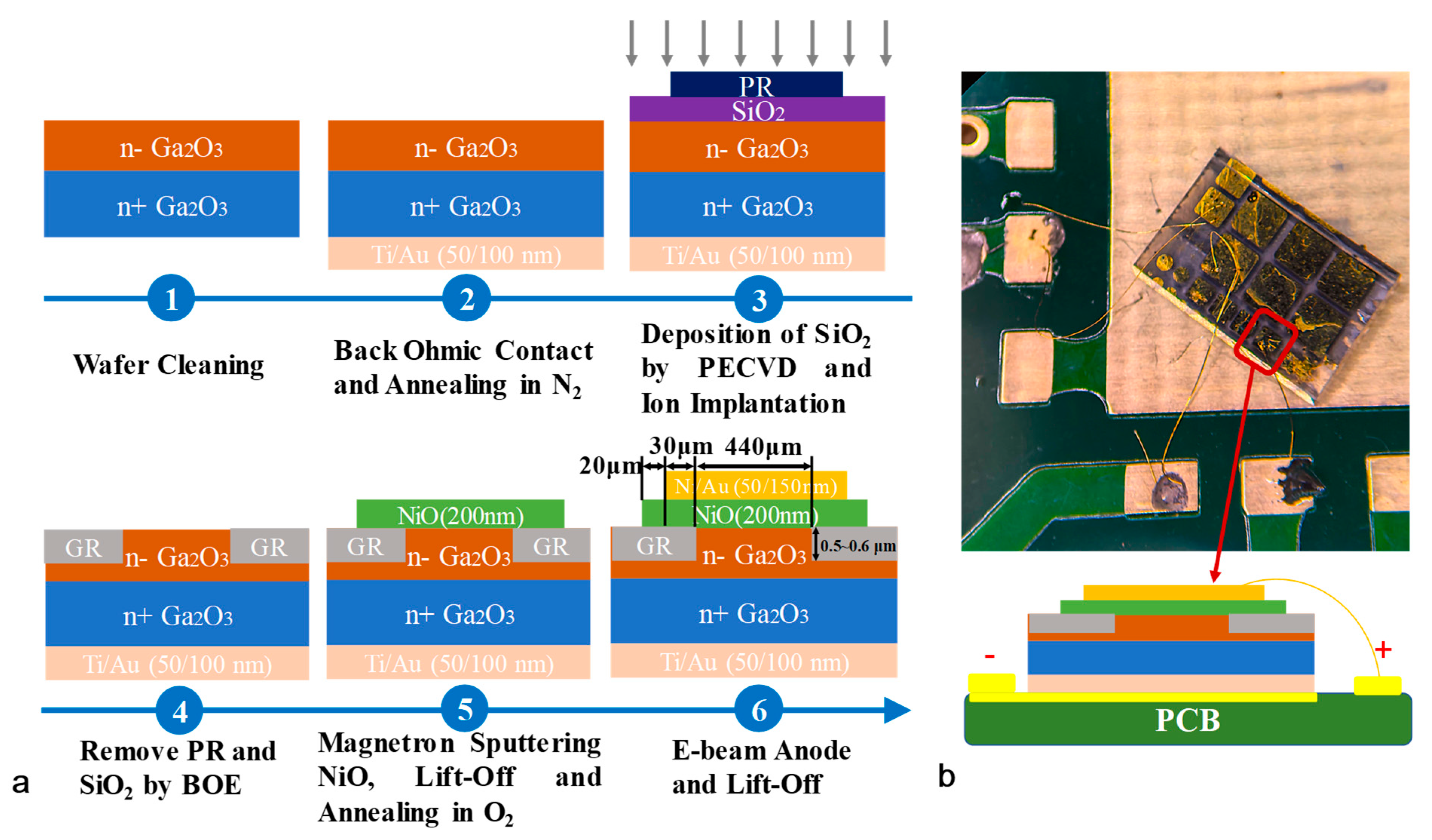
2. Experiments
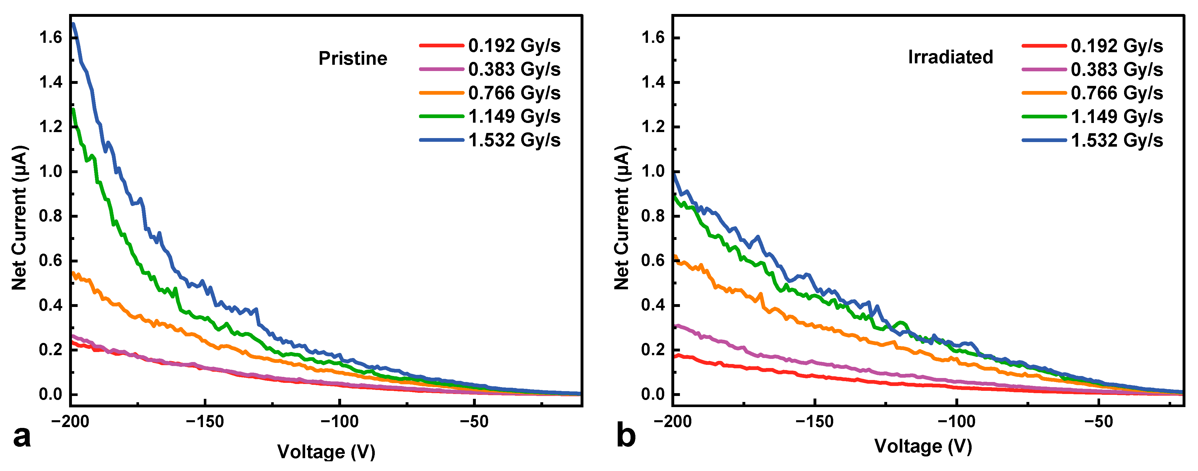
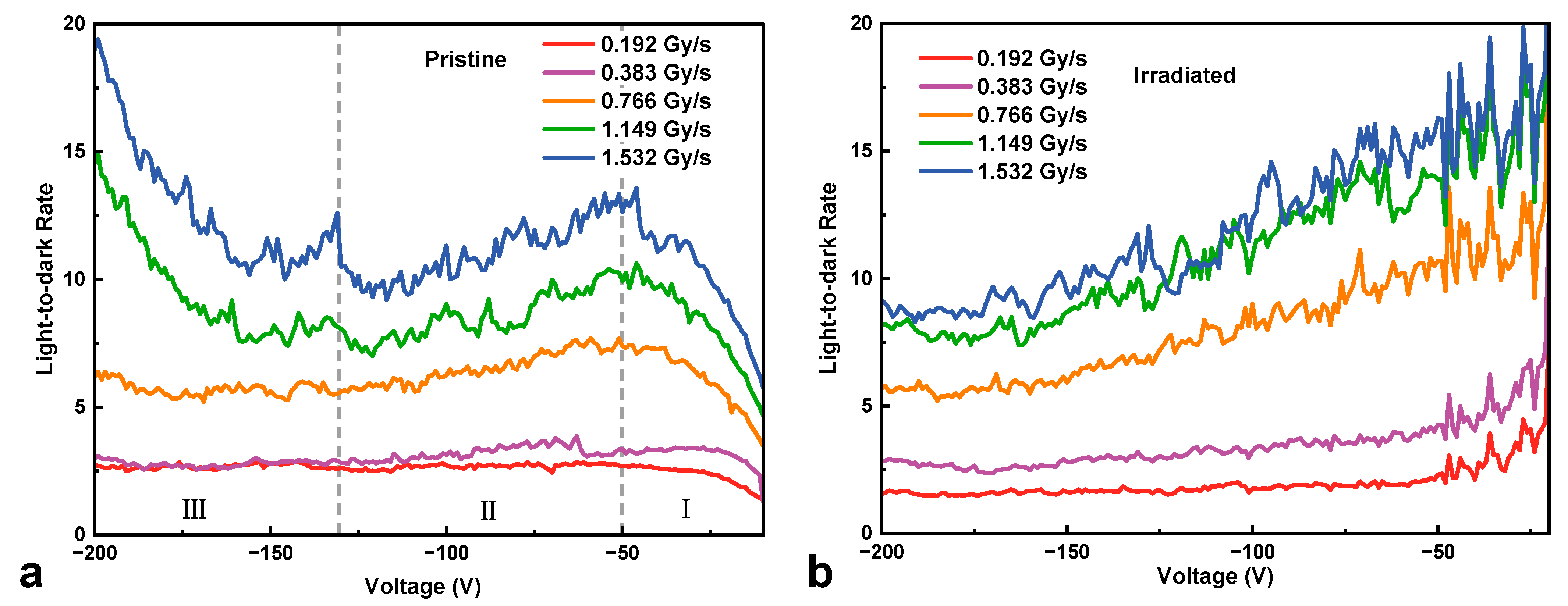
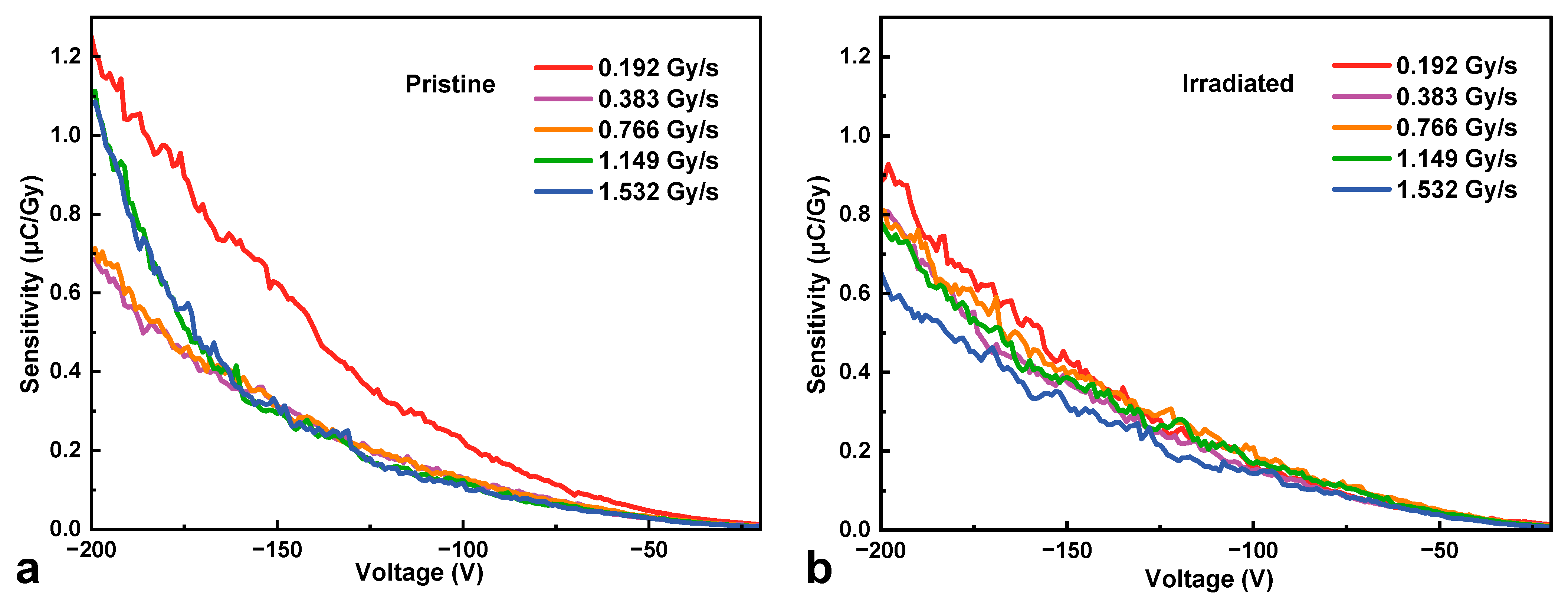
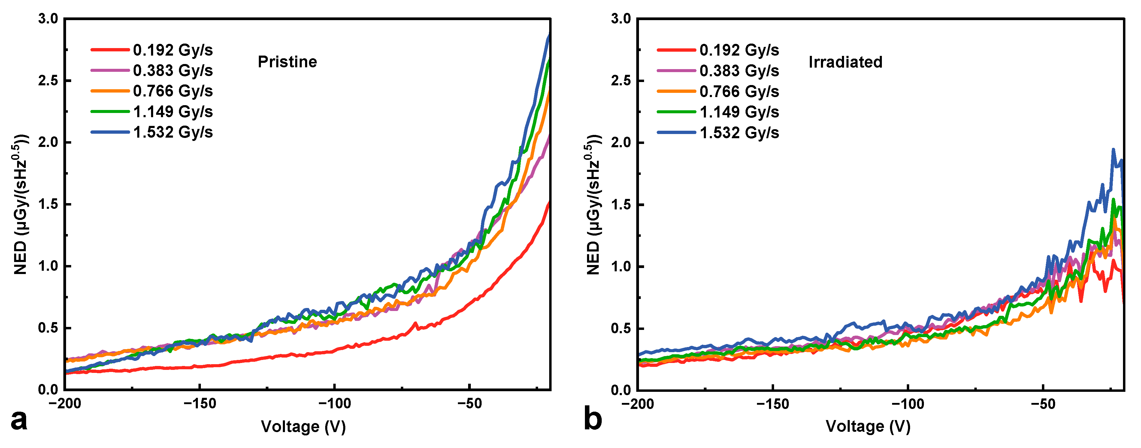
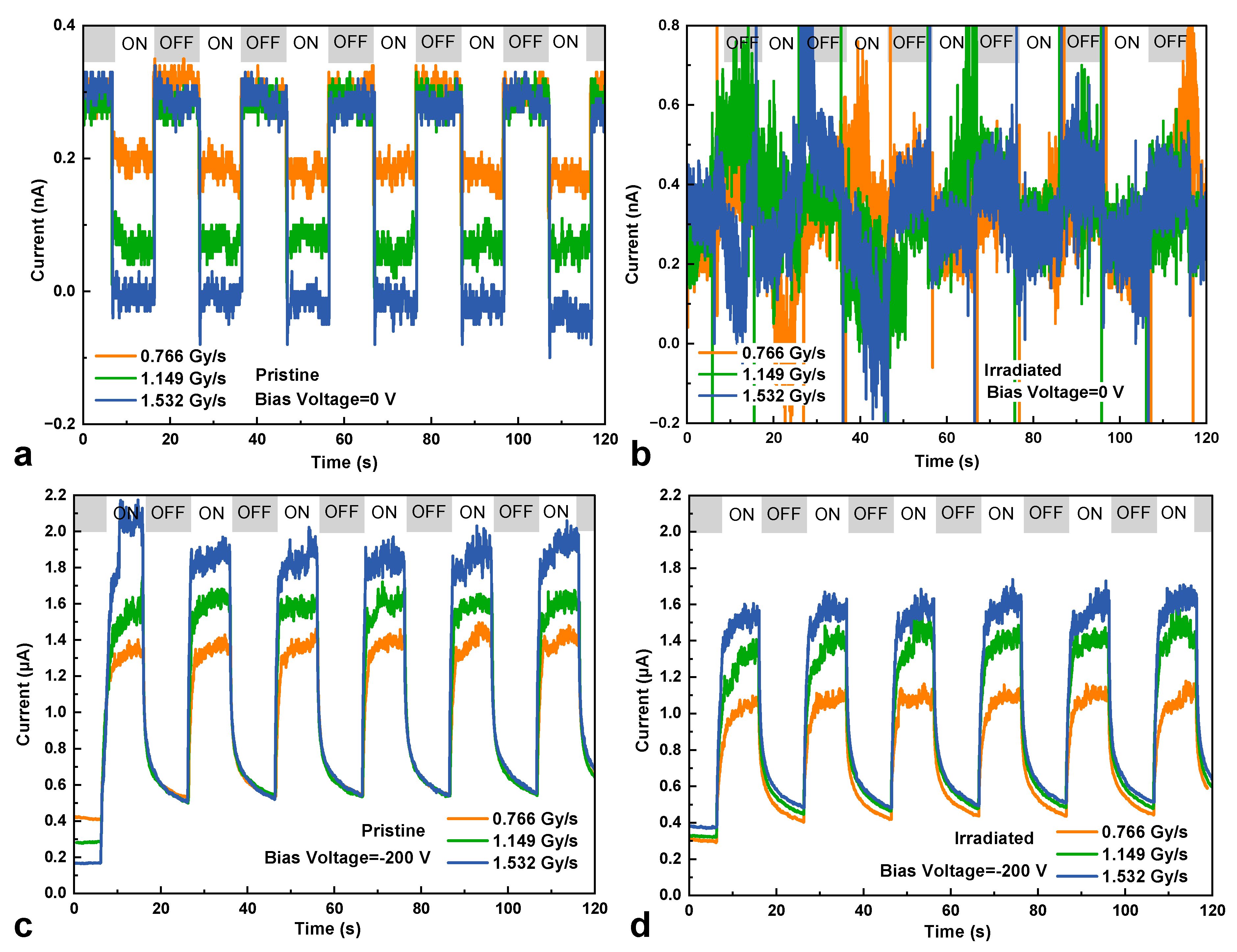
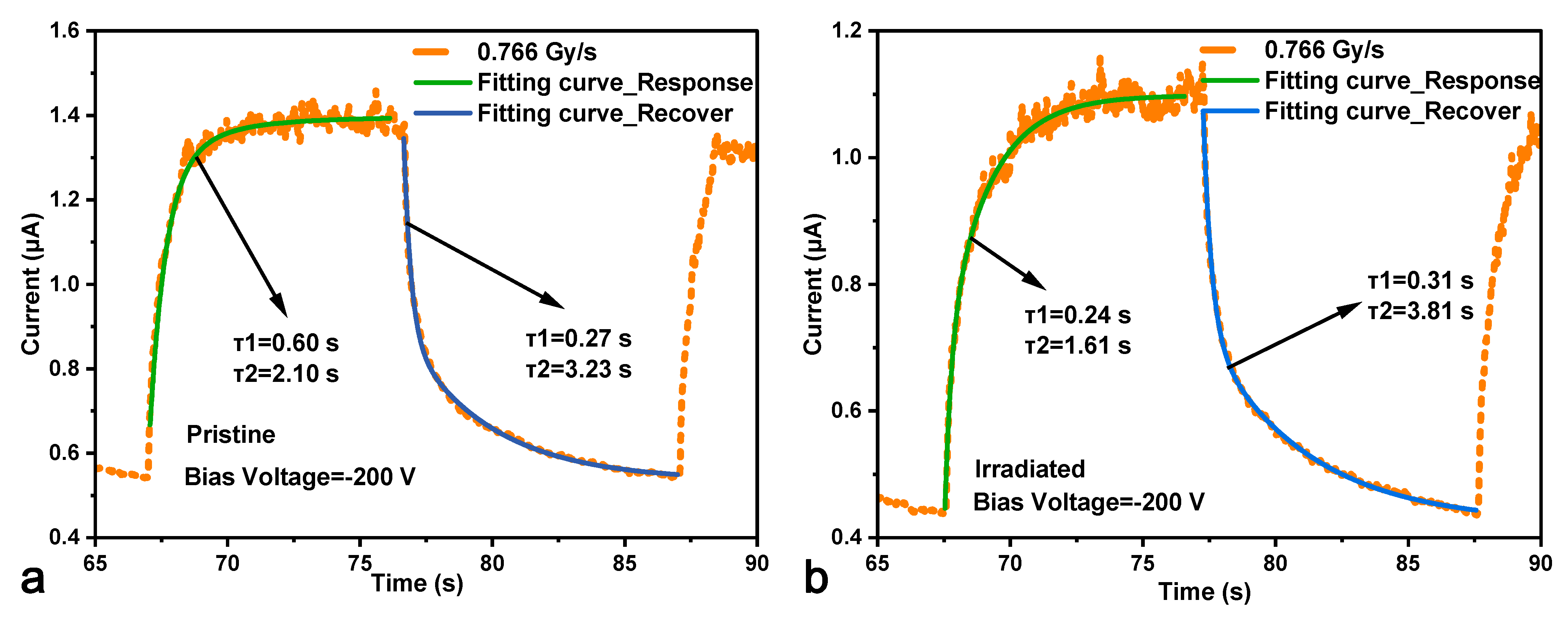
3. Results and Discussion
4. Conclusions
Author Contributions
Funding
Data Availability Statement
Acknowledgments
Conflicts of Interest
References
- Sasaki, K. Prospects for β-Ga2O3: Now and into the future. Appl. Phys. Express 2024, 17, 090101. [Google Scholar] [CrossRef]
- Pearton, S.J.; Yang, J.; Cary, P.H., IV; Ren, F.; Kim, J.; Tadjer, M.J.; Mastro, M.A. A review of Ga2O3 materials, processing, and devices. Appl. Phys. Rev. 2018, 5, 011301. [Google Scholar] [CrossRef]
- Kim, J.; Pearton, S.J.; Fares, C.; Yang, J.; Ren, F.; Kim, S.; Polyakov, A.Y. Radiation damage effects in Ga2O3 materials and devices. J. Mater. Chem. C 2019, 7, 10. [Google Scholar] [CrossRef]
- Mastro, M.A.; Kuramata, A.; Calkins, J.; Kim, J.; Ren, F.; Pearton, S.J. Perspective—Opportunities and Future Directions for Ga2O3. ECS J. Solid State Sci. Technol. 2017, 6, P356–P359. [Google Scholar] [CrossRef]
- Prasad, C.V.; Labed, M.; Shaikh, M.T.A.S.; Min, J.Y.; Nguyen, T.H.V.; Song, W.; Kim, K.J.; Rim, Y.S. Ga2O3-based X-ray detector and scintillators: A review. Mater. Today Phys. 2023, 35, 101095. [Google Scholar] [CrossRef]
- Szalkai, D.; Galazka, Z.; Irmscher, K.; Tutto, P.; Klix, A.; Gehre, D. β-Ga2O3 Solid-State Devices for Fast Neutron Detection. IEEE Trans. Nucl. Sci. 2017, 64, 1574–1579. [Google Scholar] [CrossRef]
- Lu, X.; Zhou, L.; Chen, L.; Ouyang, X.; Liu, B.; Xu, J.; Tang, H. Schottky X-ray detectors based on a bulk β-Ga2O3 substrate. Appl. Phys. Lett. 2018, 112, 103502. [Google Scholar] [CrossRef]
- Hany, I.; Yang, G.; Chung, C.-C. Fast X-ray detectors based on bulk b-Ga2O3 (Fe). J. Mater. Sci. 2020, 55, 9461–9469. [Google Scholar] [CrossRef]
- Zhou, L.; Chen, H.; Deng, Y.; Zhang, S.; Chen, L.; Lu, X.; Ouyang, X. Alpha particle detection based on a NiO/β-Ga2O3 heterojunction diode. Appl. Phys. Lett. 2023, 123, 161103. [Google Scholar] [CrossRef]
- Meng, X.; Pei, X.; Han, Y.; Sun, N.; Fang, Z.; Ren, L.; Zhang, R.; Zhang, L.; Ren, F.-F.; Feng, S.; et al. Demonstration of β-Ga2O3-Based Thermal Neutron Detector. IEEE Electron Device Lett. 2024, 46, 187–190. [Google Scholar] [CrossRef]
- Manikanthababu, N.; Sheoran, H.; Siddham, P.; Singh, R. Review of Radiation-Induced Effects on β-Ga2O3 Materials and Devices. Crystals 2022, 12, 1009. [Google Scholar] [CrossRef]
- Xia, X.; Li, J.-S.; Sharma, R.; Ren, F.; Rasel, A.J.; Stepanoff, S.; Al-Mamun, N.; Haque, A.; Wolfe, D.E.; Modak, S.; et al. Radiation Damage in the Ultra-Wide Bandgap Semiconductor Ga2O3. ECS J. Solid State Sci. Technol. 2022, 11, 095001. [Google Scholar] [CrossRef]
- Pearton, S.J.; Aitkaliyeva, A.; Xian, M.; Ren, F.; Khachatrian, A.; Ildefonsorosa, A.; Islam, Z.; Rasel, A.J.; Haque, A.; Polyakov, A.Y.; et al. Review—Radiation Damage in Wide and Ultra-Wide Bandgap Semiconductors. ECS J. Solid State Sci. Technol. 2021, 10, 055008. [Google Scholar] [CrossRef]
- Xiao, T.; Ma, T.; Lei, Z.; Fu, W.; Zhang, H.; Peng, C.; Zhang, Z.; Song, H.; Fu, Z.; Guo, D.; et al. Total Ionizing Dose Responses of β-Ga₂O₃ Thin Film Solar-Blind Ultraviolet Photodetectors. IEEE Trans. Electron Devices 2025, 72, 1249–1253. [Google Scholar] [CrossRef]
- Chen, H.; Zhou, L.; Ma, T.; Zhao, P.; Chen, L.; Yang, T.; Lei, Z.; Lu, X.; Yang, S.; Ouyang, X. Radiation effects of 5 MeV proton on Ni/β-Ga2O3 Schottky barrier diodes. APL Mater. 2024, 12, 121114. [Google Scholar] [CrossRef]
- Bonaldo, S.; Gorchichko, M.; Zhang, E.X.; Ma, T.; Mattiazzo, S.; Bagatin, M.; Paccagnella, A.; Gerardin, S.; Schrimpf, R.D.; Reed, R.A.; et al. TID Effects in Highly Scaled Gate-All-Around Si Nanowire CMOS Transistors Irradiated to Ultrahigh Doses. IEEE Trans. Nucl. Sci. 2022, 69, 1444–1452. [Google Scholar] [CrossRef]
- MacVittie, T.J.; Farese, A.M.; Jackson, W.E.I. A Systematic Review of the Hematopoietic Acute Radiation Syndrome (H-ARS) in Canines and Non-Human Primates: Acute Mixed Neutron/Gamma vs. Reference Quality Radiations. Health Phys. 2020, 119, 527–558. [Google Scholar] [CrossRef]
- Ma, T.; Bonaldo, S.; Mattiazzo, S.; Baschirotto, A.; Enz, C.; Paccagnella, A.; Gerardin, S. Influence of Fin and Finger Number on TID Degradation of 16-nm Bulk FinFETs Irradiated to Ultrahigh Doses. IEEE Trans. Nucl. Sci. 2022, 69, 307–313. [Google Scholar] [CrossRef]
- Khan, S.A.; Saha, S.; Singisetti, U.; Bhuiyan, A.F.M.A.U. Radiation resilience of β-Ga2O3 Schottky barrier diodes under high dose gamma radiation. J. Appl. Phys. 2024, 136, 225701. [Google Scholar] [CrossRef]
- Fu, W.; Ma, T.; Lei, Z.; Peng, C.; Zhang, H.; Zhang, Z.; Xiao, T.; Song, H.; Wang, Y.; Wang, J.; et al. Temperature Dependence of Total Ionizing Dose Effects of β-Ga2O3 Schottky Barrier Diodes. Electronics 2024, 13, 2215. [Google Scholar] [CrossRef]
- Wong, M.H.; Takeyama, A.; Makino, T.; Ohshima, T.; Sasaki, K.; Kuramata, A.; Yamakoshi, S.; Higashiwaki, M. Radiation hardness of β-Ga2O3 metal oxide-semiconductor field-effect transistors against gamma-ray irradiation. Appl. Phys. Lett. 2018, 112, 023503. [Google Scholar] [CrossRef]
- Gong, H.; Liao, W.; Zhang, E.X.; Sternberg, A.L.; McCurdy, M.W.; Davidson, J.L.; Reed, R.A.; Fleetwood, D.M.; Schrimpf, R.D.; Shuvra, P.D.; et al. Proton-Induced Displacement Damage and Total-Ionizing-Dose Effects on Silicon-Based MEMS Resonators. IEEE Trans. Nucl. Sci. 2018, 65, 34–38. [Google Scholar] [CrossRef]
- Zhang, S.; Deng, Y.; Chen, L.; He, S.; Du, X.; Wang, F.; Lai, Y.; Zhong, S.; Zhao, N.; Li, Y.; et al. Pulsed X-Ray Detector Based on Vertical p-NiO/β-Ga2O3 Heterojunction Diode. Phys. Status Solidi B 2024, 2400363. [Google Scholar] [CrossRef]
- Zhang, P.; Ang, Y.S.; Garner, A.L.; Valfells, Á.; Luginsland, J.W.; Ang, L.K. Space–charge limited current in nanodiodes: Ballistic, collisional, and dynamical effects. J. Appl. Phys. 2021, 129, 100902. [Google Scholar] [CrossRef]
- Lu, X.; Zhou, L.; Chen, L.; Ouyang, X.; Tang, H.; Liu, B.; Xu, J. X-ray Detection Performance of Vertical Schottky Photodiodes Based on a Bulk β-Ga2O3 Substrate Grown by an EFG Method. ECS J. Solid State Sci. Technol. 2019, 8, Q3046–Q3049. [Google Scholar] [CrossRef]
- Yeargan, J.R.; Taylor, H.L. The Poole-Frenkel Effect with Compensation Present. J. Appl. Phys. 1968, 39, 5600–5604. [Google Scholar] [CrossRef]
- Schmitz, G.; Gassmann, P.; Franchy, R. A combined scanning tunneling microscopy and electron energy loss spectroscopy study on the formation of thin, well-ordered β-Ga2O3 films on CoGa(001). J. Appl. Phys. 1998, 83, 2533–2538. [Google Scholar] [CrossRef]
- Xu, W.; Shen, Z.; Qu, Z.; Zhao, T.; Yi, A.; You, T.; Han, G.; Ou, X. Current transport mechanism of lateral Schottky barrier diodes on β-Ga2O3/SiC structure with atomic level interface. Appl. Phys. Lett. 2024, 124, 112102.112101–112102.112107. [Google Scholar] [CrossRef]
- Huang, Y.; Xu, X.; Yang, J.; Yu, X.; Wei, Y.; Ying, T.; Liu, Z.; Jing, Y.; Li, W.; Li, X. Library of intrinsic defects in β-Ga2O3: First-principles studies. Mater. Today Commun. 2023, 35, 105898. [Google Scholar] [CrossRef]


| Parameters | Pristine (Res./Rec.) | Irradiated (Res./Rec.) |
|---|---|---|
| Response time | 2.92 s | 4.37 s |
| Recovery time | 5.03 s | 5.16 s |
| Parameters | Irradiated |
|---|---|
| ε∞ | 2.27 |
| qϕt | 1.07 eV |
Disclaimer/Publisher’s Note: The statements, opinions and data contained in all publications are solely those of the individual author(s) and contributor(s) and not of MDPI and/or the editor(s). MDPI and/or the editor(s) disclaim responsibility for any injury to people or property resulting from any ideas, methods, instructions or products referred to in the content. |
© 2025 by the authors. Licensee MDPI, Basel, Switzerland. This article is an open access article distributed under the terms and conditions of the Creative Commons Attribution (CC BY) license (https://creativecommons.org/licenses/by/4.0/).
Share and Cite
Ouyang, X.; Zhang, S.; Bai, T.; Chen, Z.; Deng, Y.; Zhou, L.; Song, X.; Chen, H.; Lai, Y.; Lu, X.; et al. Performance Degradation of Ga2O3-Based X-Ray Detector Under Gamma-Ray Irradiation. Micromachines 2025, 16, 339. https://doi.org/10.3390/mi16030339
Ouyang X, Zhang S, Bai T, Chen Z, Deng Y, Zhou L, Song X, Chen H, Lai Y, Lu X, et al. Performance Degradation of Ga2O3-Based X-Ray Detector Under Gamma-Ray Irradiation. Micromachines. 2025; 16(3):339. https://doi.org/10.3390/mi16030339
Chicago/Turabian StyleOuyang, Xiao, Silong Zhang, Tao Bai, Zhuo Chen, Yuxin Deng, Leidang Zhou, Xiaojing Song, Hao Chen, Yuru Lai, Xing Lu, and et al. 2025. "Performance Degradation of Ga2O3-Based X-Ray Detector Under Gamma-Ray Irradiation" Micromachines 16, no. 3: 339. https://doi.org/10.3390/mi16030339
APA StyleOuyang, X., Zhang, S., Bai, T., Chen, Z., Deng, Y., Zhou, L., Song, X., Chen, H., Lai, Y., Lu, X., Chen, L., Miao, L., & Ouyang, X. (2025). Performance Degradation of Ga2O3-Based X-Ray Detector Under Gamma-Ray Irradiation. Micromachines, 16(3), 339. https://doi.org/10.3390/mi16030339