
An Overview of Hot Carrier Degradation on Gate-All-Around Nanosheet Transistors
Abstract
1. Introduction
2. Structure, HCD Characterization Results, and Discussion
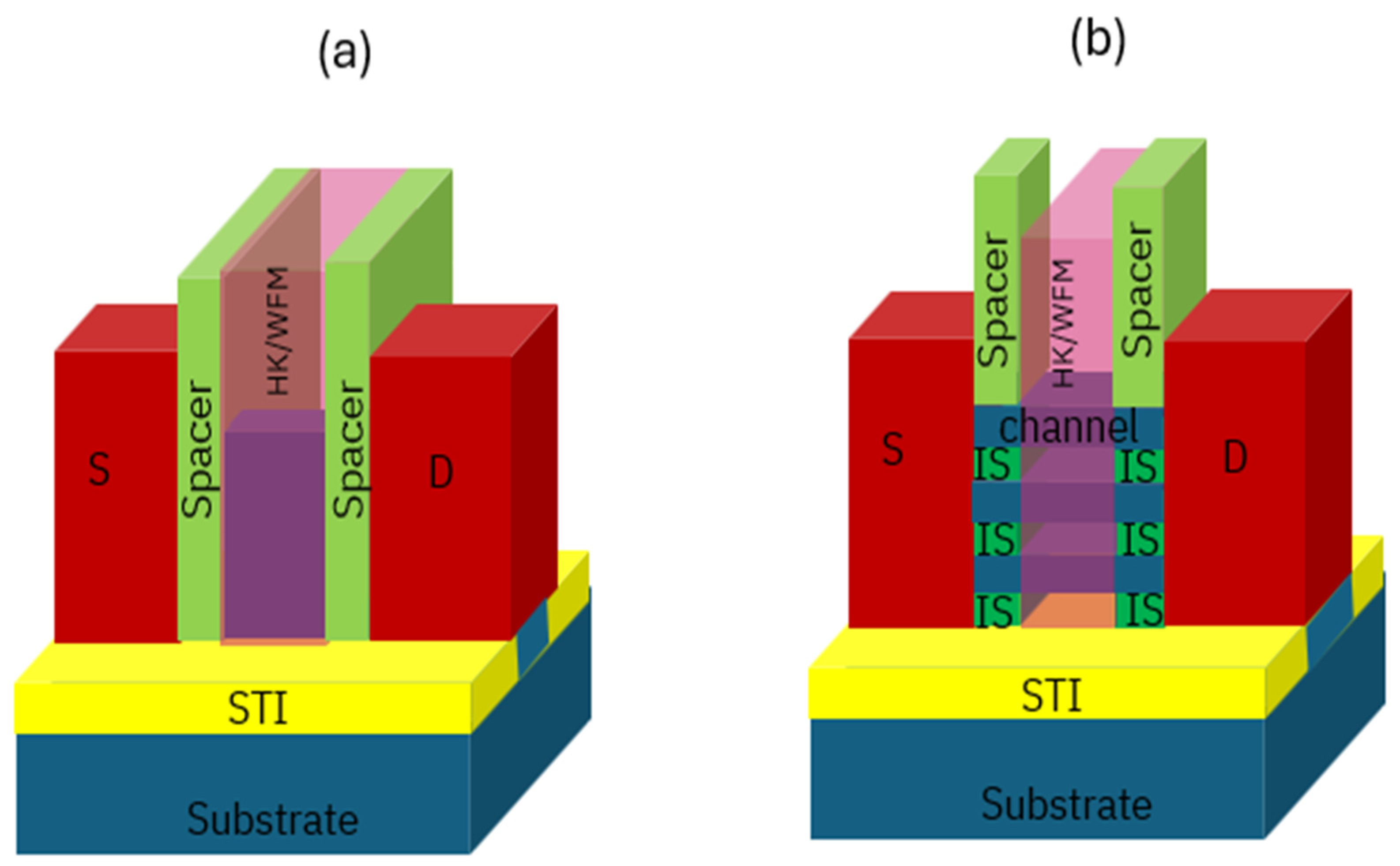
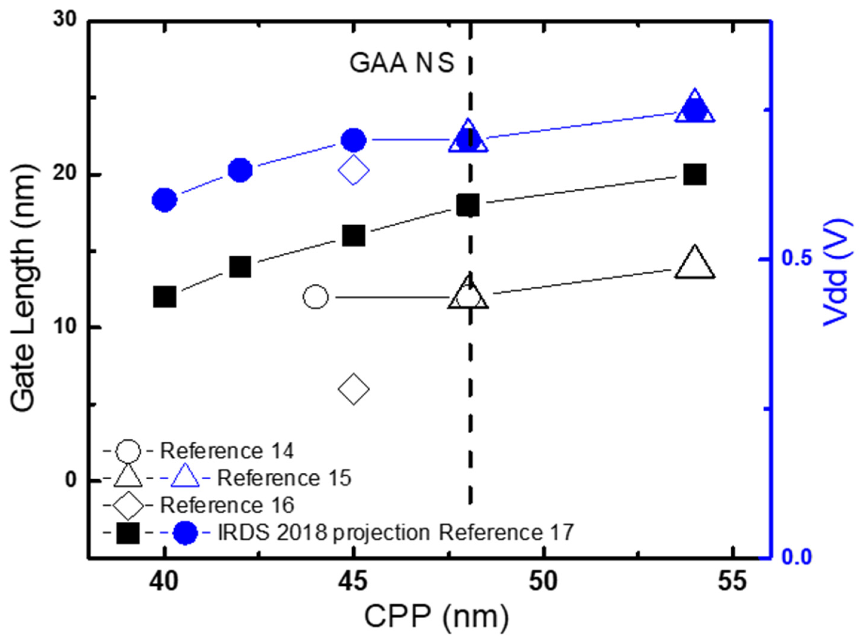
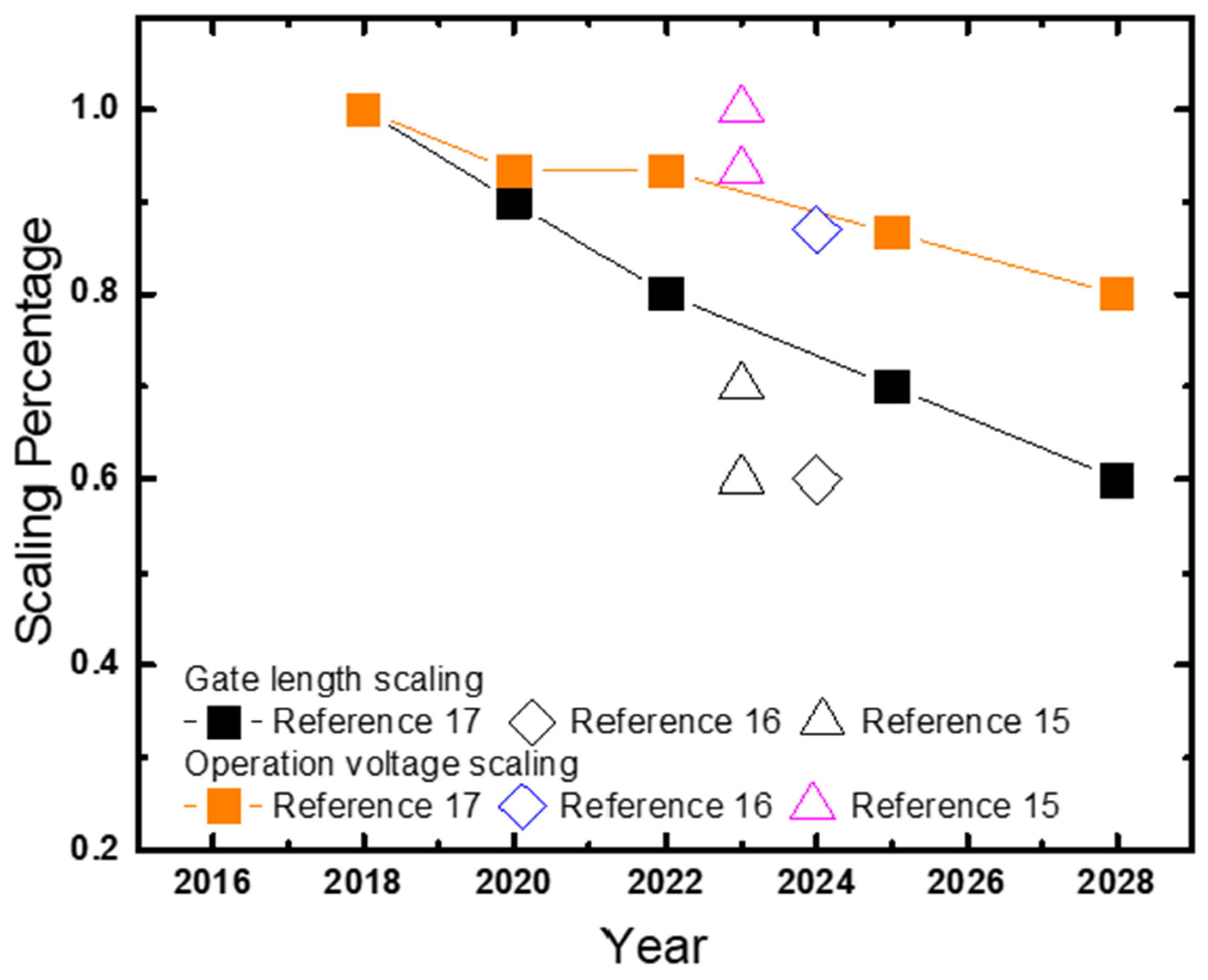
2.1. GAA NS Structures and Gate Length Scaling
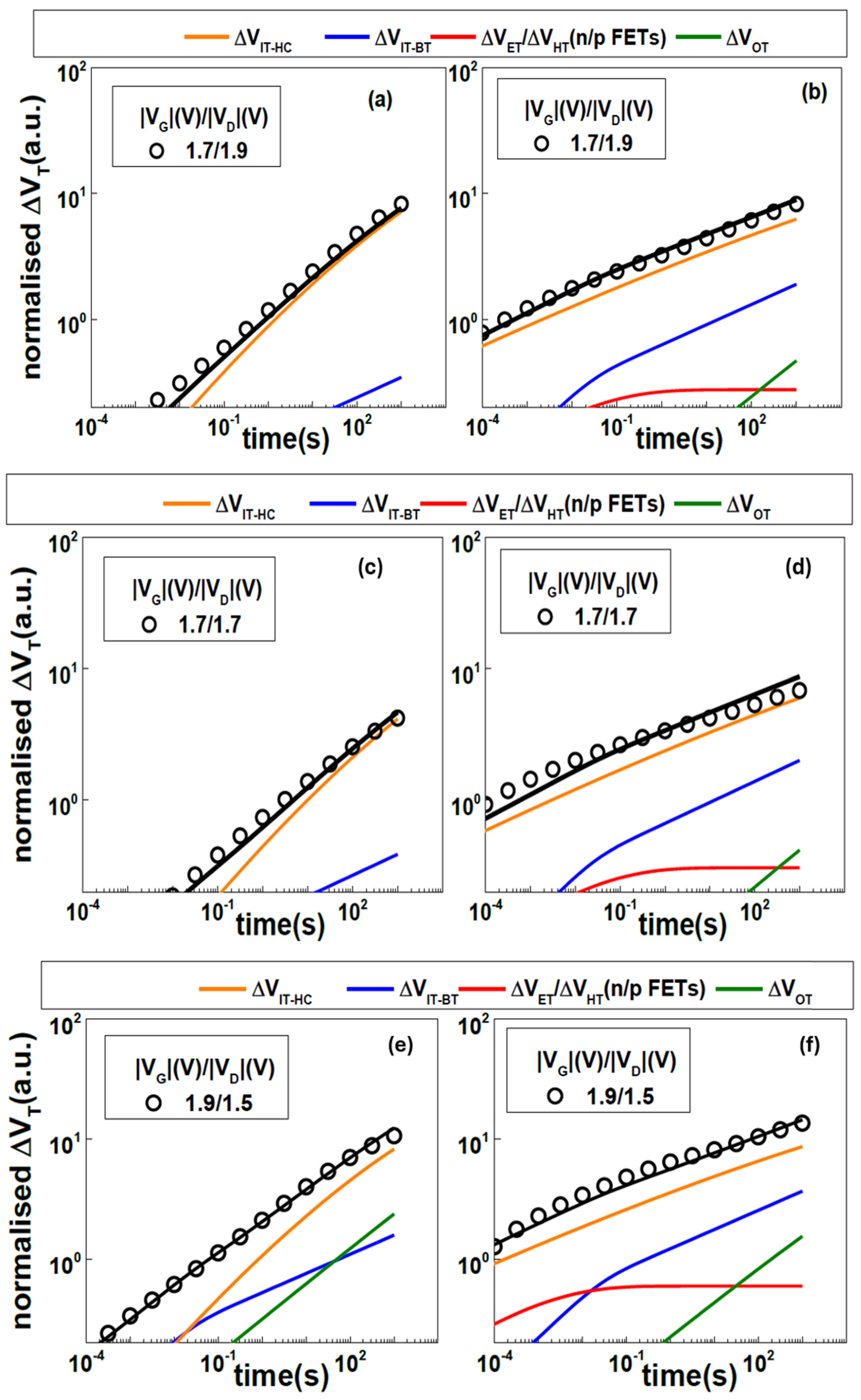
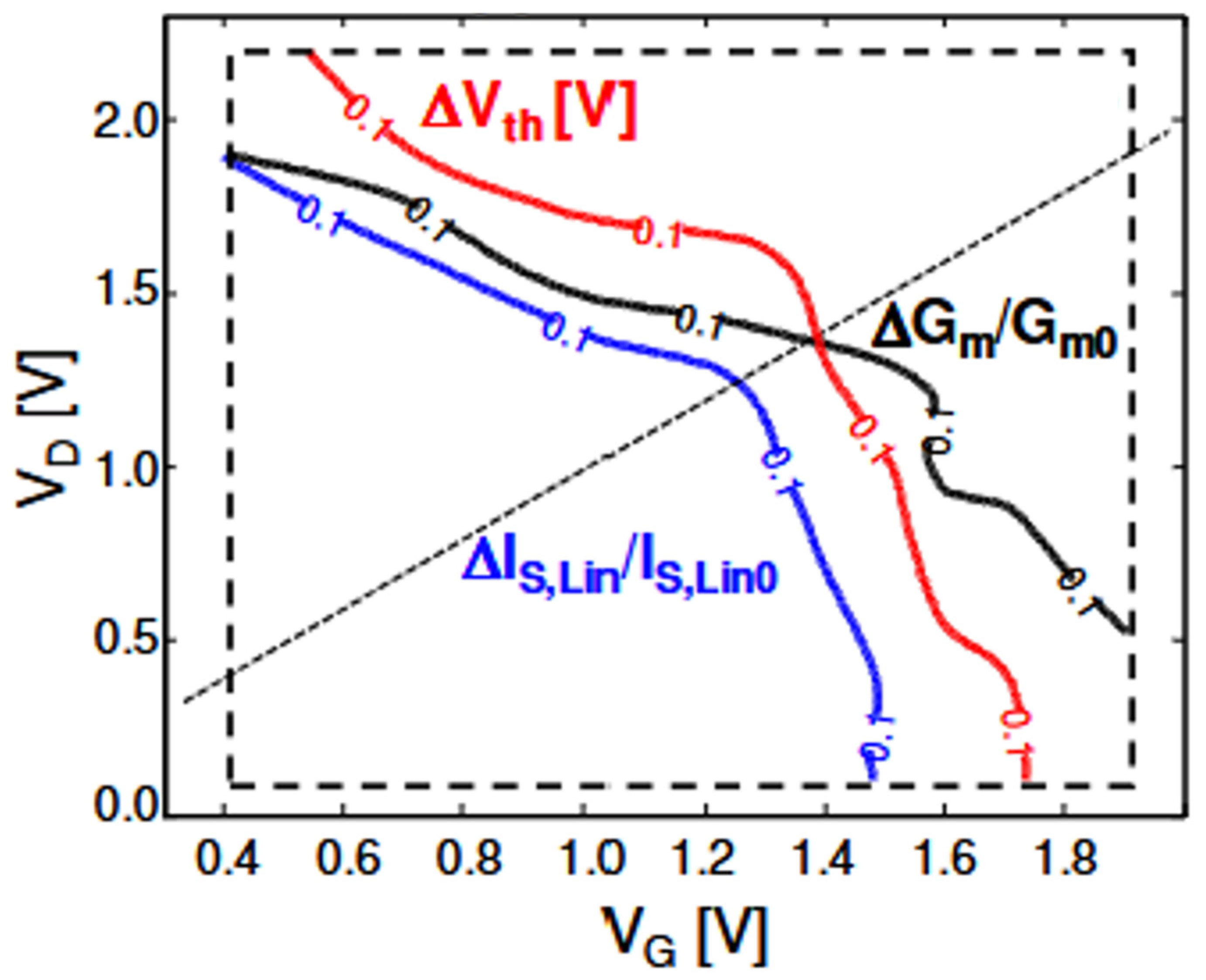
2.2. HCD Characterization
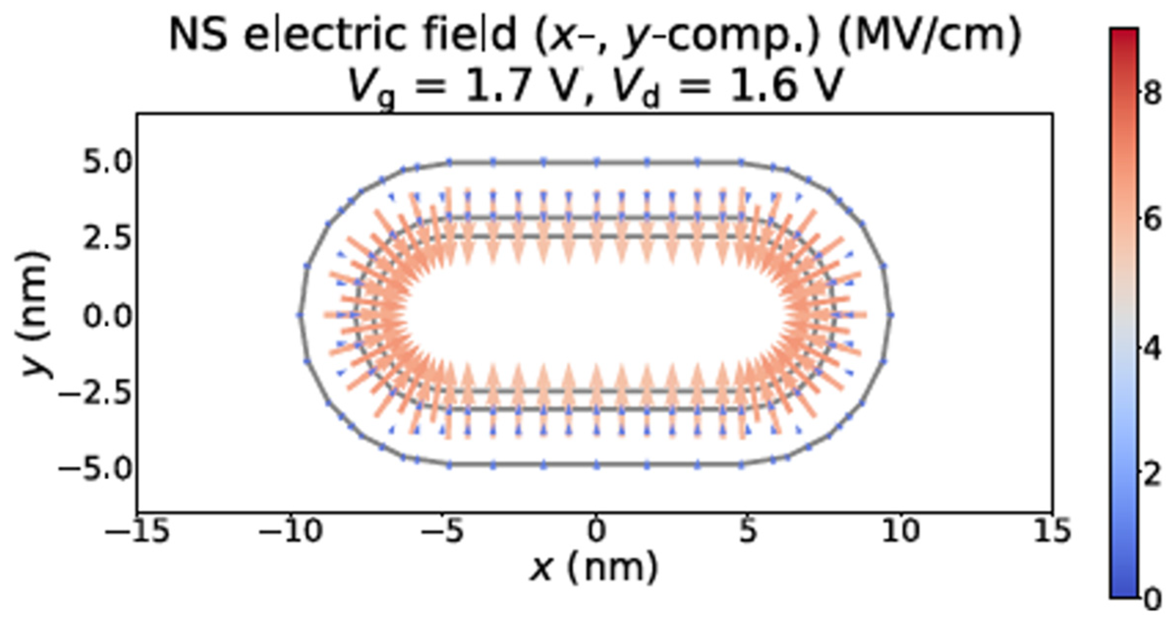
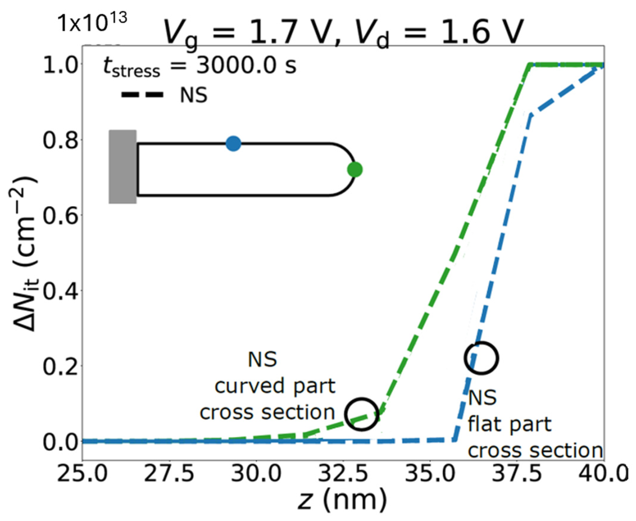
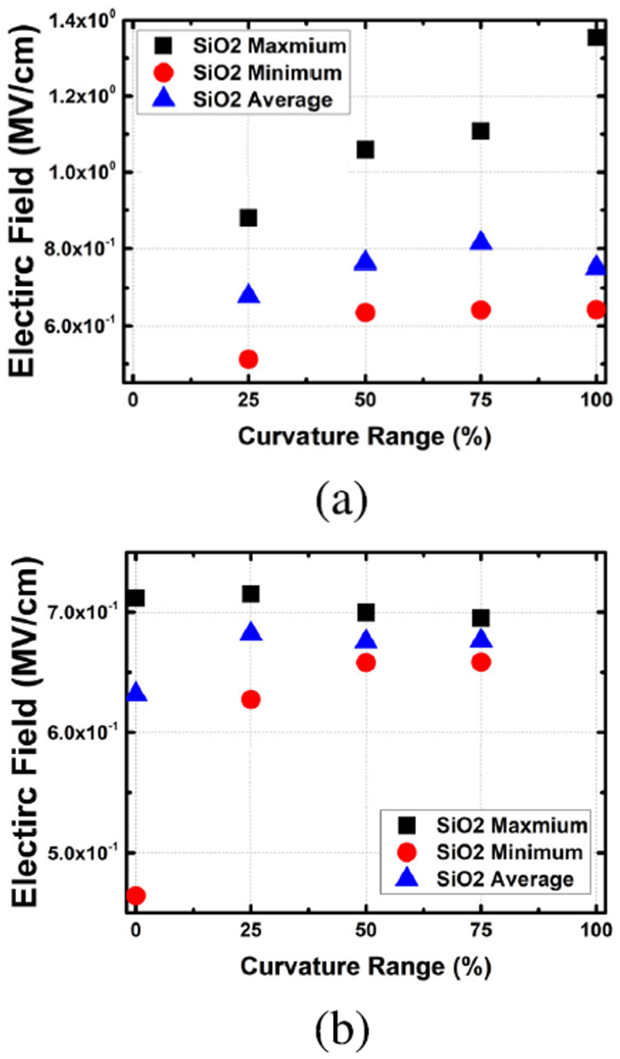
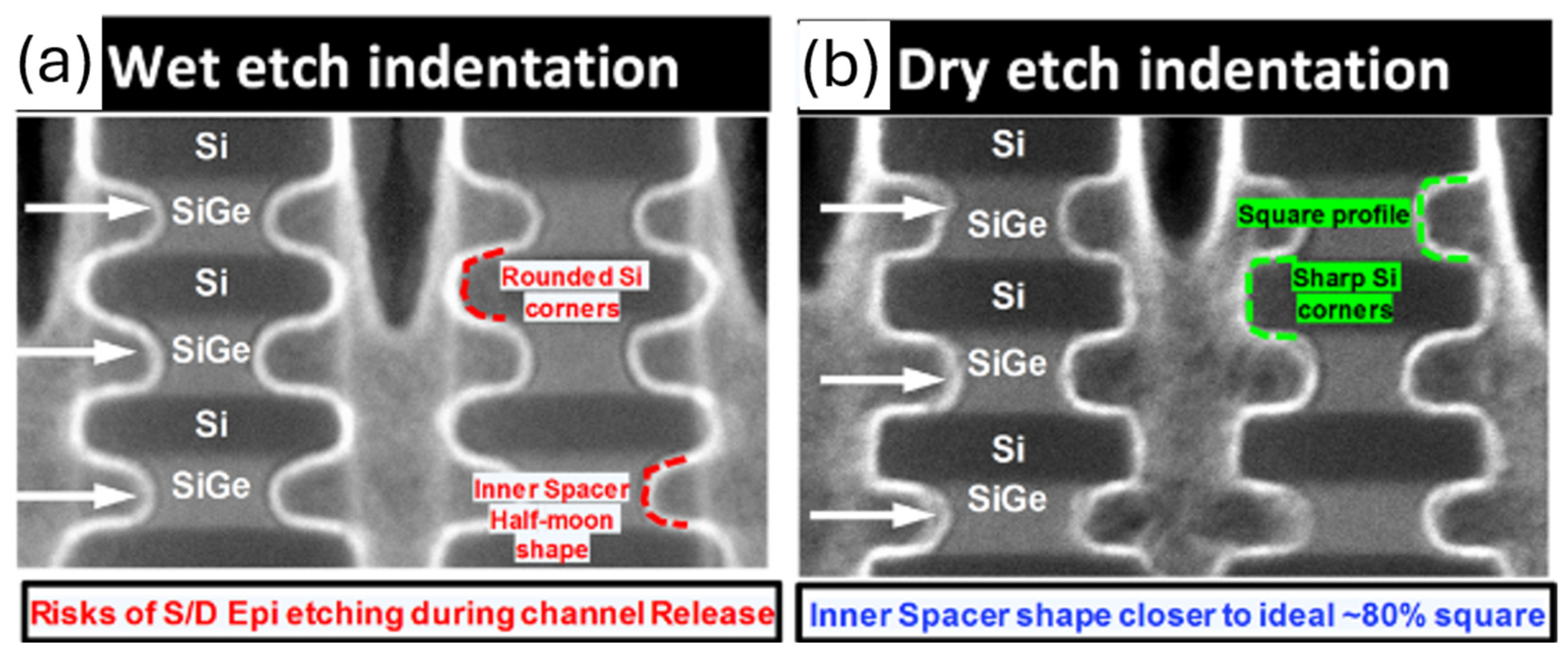
2.3. Corner Effects
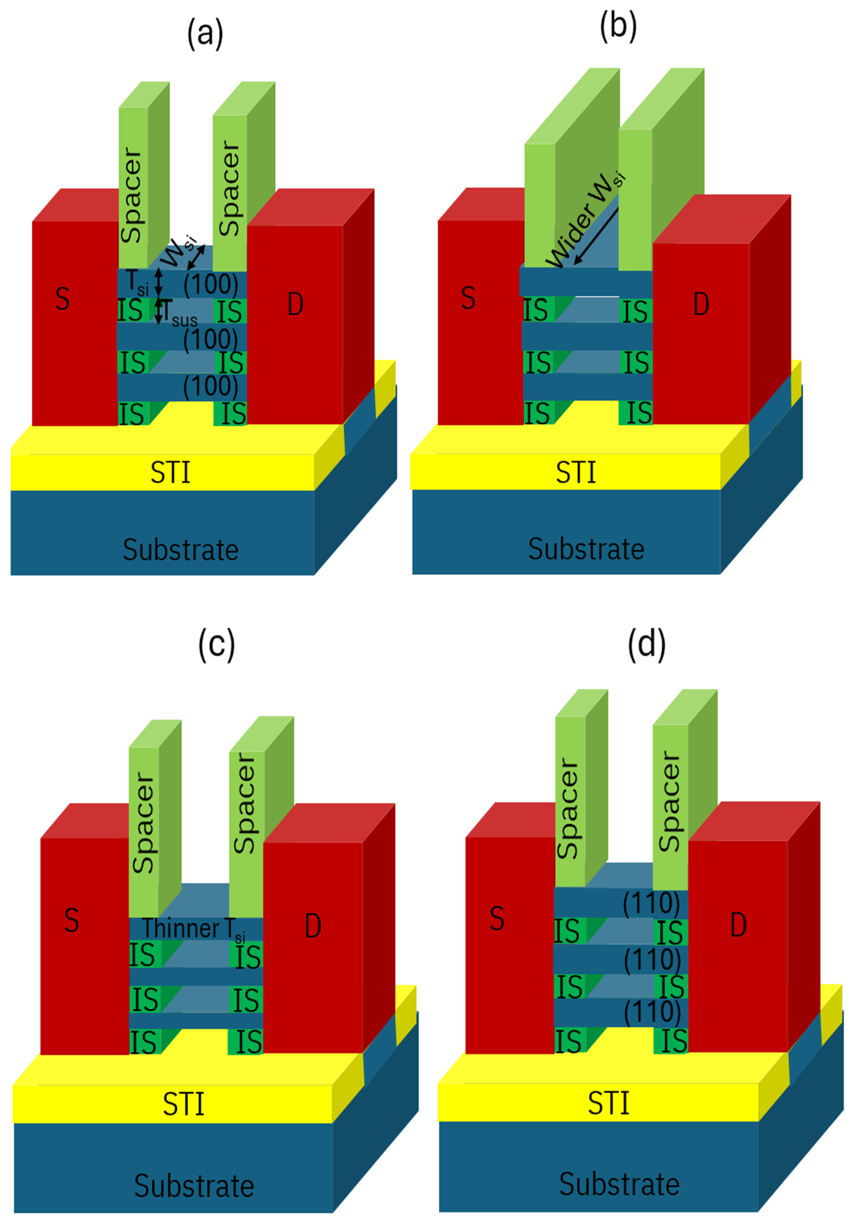
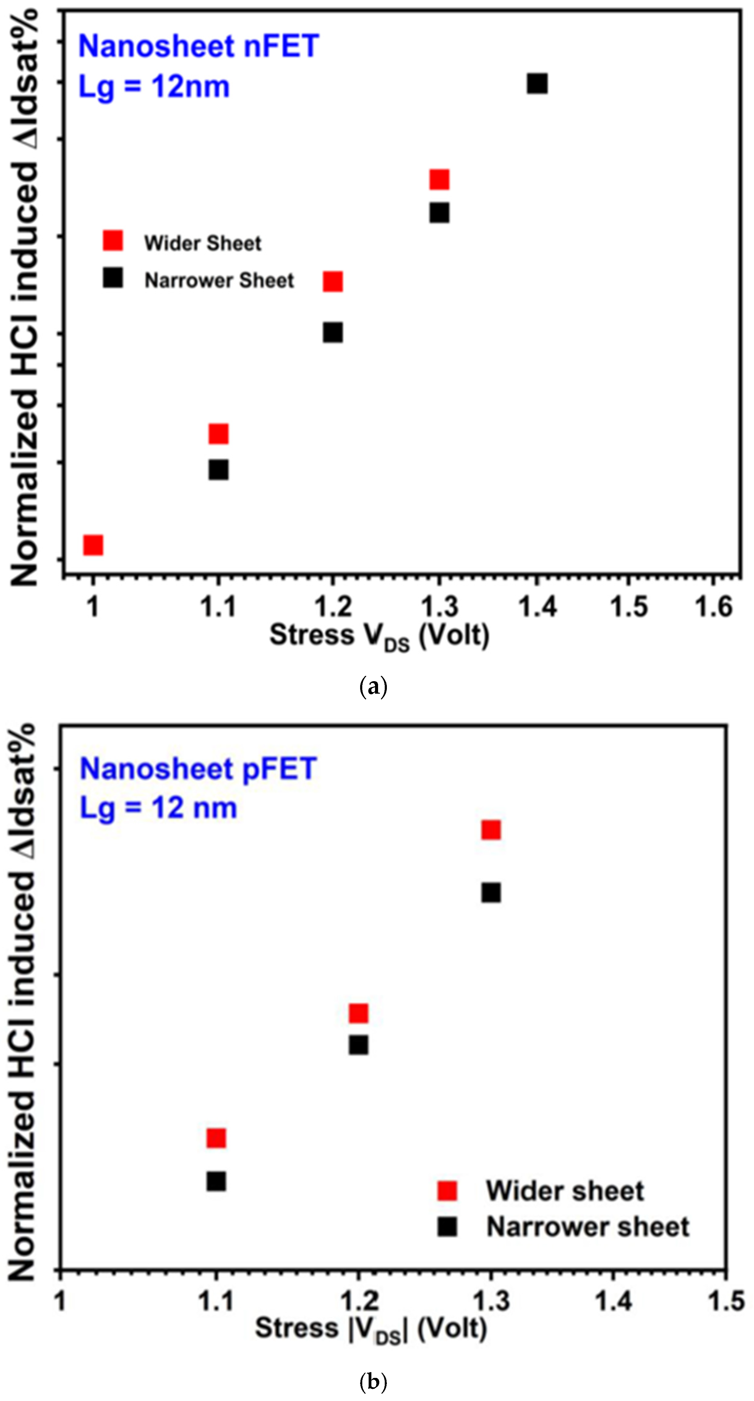
2.4. Geometry (Wsi, Tsi) and Surface Orientation Effect
2.5. Inner Spacer and Junction Dependent
2.6. Dielectric Wall Effect (Fork Sheet Specific)
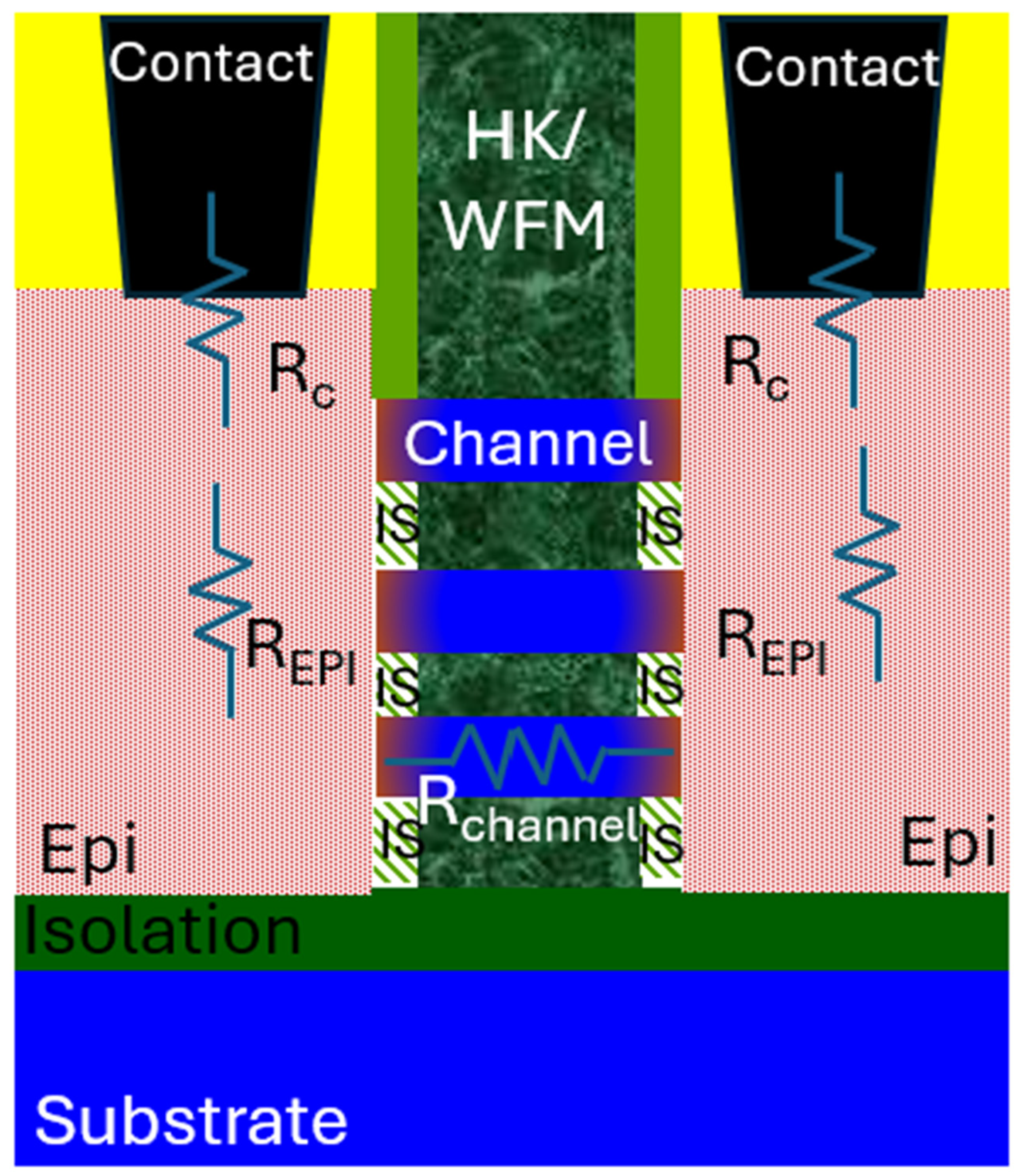
2.7. Body Isolation Effect
2.8. HCD and Self-Heating
3. Challenges and Future Outlook
Funding
Data Availability Statement
Acknowledgments
Conflicts of Interest
References
- Bangsaruntip, S.; Cohen, G.M.; Majumdar, A.; Zhang, Y.; Engelmann, S.U.; Fuller, N.C.M.; Gignac, L.M.; Mittal, S.; Newbury, J.S.; Guillorn, M.; et al. High Performance and Highly Uniform Gate-All-Around Silicon Nanowire MOSFETs with Wire Size Dependent Scaling. In Proceedings of the IEEE International Electron Devices Meeting (IEDM), Baltimore, MD, USA, 7–9 December 2009; pp. 1–4. [Google Scholar]
- Kim, S.; Guillorn, M.; Lauer, I.; Oldiges, P.; Hook, T.; Na, M. Performance Trade-offs in FinFET and Gate-All-Around Device Architectures for 7 nm-node and beyond. In Proceedings of the S3S Conference, Rohnert Park, CA, USA, 5–8 October 2015; pp. 1–3. [Google Scholar]
- Mertens, H.; Ritzenthaler, R.; Chasin, A.; Schram, T.; Kunnen, E.; Hikavyy, A.; Ragnarsson, L.-Å.; Dekkers, H.; Hopf, T.; Wostyn, K.; et al. Vertically Stacked Gate-All-Around Si Nanowire CMOS Transistors with Dual Work Function Metal Gates. In Proceedings of the IEEE International Electron Devices Meeting (IEDM), San Francisco, CA, USA, 3–7 December 2016; pp. 19–27. [Google Scholar]
- Lauer, I.; Loubeta, N.; Kim, B.S.D.; Ott, J.A.; Mignot, C.S.; Venigallab, R.; Yamashitab, T.; Standaertb, T.; Faltermeierb, J.; Basker, B.V.; et al. Si Nanowire CMOS Fabricated with Minimal Deviation from RMG FinFET Technology Showing Record Performance. In IEEE Symposium on VLSI Technology and Circuits (VLSI Technology and Circuits); IEEE: New York, NY, USA, 2015; p. T141. [Google Scholar]
- IEEE. International Roadmap for Devices and Systems More Moore: 2015; IEEE: Piscataway, NJ, USA, 2015; pp. 1–31. [Google Scholar]
- Yeap, G.; Lin, S.S.; Shang, H.L.; Lin, H.C.; Peng, Y.C.; Wang, M.; Wang, P.W.; Lin, C.P.; Lin, C.P.; Yu, K.F.; et al. 2nm Platform Technology featuring Energy-efficient Nanosheet Transistors and Interconnects co-optimized with 3DIC for AI, HPC and Mobile SoC Applications. In Proceedings of the IEEE International Electron Devices Meeting (IEDM), San Francisco, CA, USA, 7–11 December 2024; p. T2-1. [Google Scholar]
- Chen, W.C.; Chen, S.H.; Hellings, G.; Bury, E.; Simicic, M.; Wu, Z.; Van der Plas, G.; Groeseneken, G.; Beyne, E. External I/O interfaces in sub-5 nm GAA NS Technology and STCO Scaling Options. In Proceedings of the IEEE Symposium on VLSI Technology and Circuits (VLSI Technology and Circuits), Kyoto, Japan, 13–19 June 2021; pp. 1–2. [Google Scholar]
- Sun, Z.; Wang, Z.; Wang, R.; Huang, R. Investigation of Sheet Width Dependence on Hot Carrier Degradation in GAA Nanosheet Transistors. In Proceedings of the IEEE Silicon Nanoelectronics Workshop (SNW), Honolulu, HI, USA, 15–16 June 2024; pp. 49–50. [Google Scholar]
- Mahapatra, S.; Diwakar, H.; Thakor, K.; Choudhury, N.; Chatterjee, P.; Kumar, S.; Singhal, U.; Sharma, U. A Generic Framework for MOSFET Reliability—Part II: Gate and Drain Stress—HCD. IEEE Trans. Electron Devices 2024, 71, 126–137. [Google Scholar] [CrossRef]
- Sharma, U.; Mahapatra, S. Modeling of HCD Kinetics Under Full V G-D Space, Different Experimental Conditions and Across Different Device Architectures. J. Electron Devices Soc. 2020, 8, 1354–1362. [Google Scholar] [CrossRef]
- Laurent, A.; Garros, X.; Barraud, S.; Mariniello, G.; Reimbold, G.; Roy, D.; Vincent, E.; Ghibaudo, G. Hot Carrier Degradation in Nanowire Transistors: Physical mechanisms, Width dependence and Impact of Self-Heating. In Proceedings of the IEEE Symposium on VLSI Technology and Circuits (VLSI Technology and Circuits), Honolulu, HI, USA, 14–16 June 2016. [Google Scholar]
- Barraud, S.; Previtali, B.; Vizioz, C.; Hartmann, J.-M.; Sturm, J.; Lassarre, J.; Perrot, C.; Rodriguez, P.; Loup, V.; Magalhaes-Lucas, A.; et al. 7-Levels-Stacked Nanosheet GAA Transistors for High Performance Computing. In Proceedings of the IEEE Symposium on VLSI Technology and Circuits (VLSI Technology and Circuits), Honolulu, HI, USA, 16–19 June 2020. [Google Scholar]
- Chen, S.; Ma, Y.; Su, H.; Fan, X.; Liu, Y. Few-Mode Fiber-Based Long-Period Fiber Gratings: A Review. J. Opt. Photonics Res. 2024, 1, 2–15. [Google Scholar] [CrossRef]
- Loubet, N.; Hook, T.; Montanini, P.; Yeung, C.-W.; Kanakasabapathy, S.; Guillorn, M.; Yamashita, T.; Zhang, J.; Miao, X.; Wang, J.; et al. Stacked Nanosheet Gate-All-Around Transistor to Enable Scaling Beyond FinFET. In Proceedings of the IEEE Symposium on VLSI Technology and Circuits (VLSI Technology and Circuits), Kyoto, Japan, 5–8 June 2017; pp. T230–T231. [Google Scholar]
- Kim, S.; Park, H.; Choi, E.; Kim, Y.H.; Kim, D.; Shim, H.; Chung, S.; Jung, P. Reliability Assessment of 3nm GAA Logic Technology Featuring Multi-Bridge-Channel FETs. In Proceedings of the IEEE International Reliability Physics Symposium (IRPS), Monterey, CA, USA, 26–30 March 2023; pp. 8A1-1–8A1-8. [Google Scholar]
- Agrawal, A.; Chakraborty, W.; Li, W.; Ryu, H.; Markman, B.; Sung, S.H.; Paul, R.; Huang, C.Y.; Choi, S.M.; Rho, K.; et al. Silicon RibbonFET CMOS at 6nm Gate Length. In Proceedings of the IEEE International Electron Devices Meeting (IEDM), San Francisco, CA, USA, 7–11 December 2024; p. T2-2. [Google Scholar]
- International Roadmap for Devices and Systems More Moore: 2020; IEEE: Piscataway, NJ, USA, 2020; pp. 1–31.
- Arfaoui, W.; Federspiel, X.; Mora, P.; Monsieur, F.; Cacho, F.; Roy, D.; Bravaix, A. Energy-driven Hot-Carrier model in advanced nodes. In Proceedings of the IEEE International Reliability Physics Symposium (IRPS), Waikoloa, HI, USA, 1–5 June 2014; pp. XT.12.1–XT.12.5. [Google Scholar]
- Mahapatra, S.; Sharma, U. A Review of Hot Carrier Degradation in n-Channel MOSFETs—Part I: Physical Mechanism. IEEE Trans. Electron Devices 2020, 67, 2660–2671. [Google Scholar] [CrossRef]
- Jech, M.; Rott, G.; Reisinger, H.; Tyaginov, S.; Rzepa, G.; Grill, A.; Jabs, D.; Jungemann, C.; Waltl, M.; Grasser, T. Mixed Hot-Carrier/Bias Temperature Instability Degradation Regimes in Full {VG, VD} Bias Space: Implictions and peculiarities. IEEE Trans. Electron Devices 2020, 67, 3315–3322. [Google Scholar] [CrossRef]
- Zhou, H.; Hasanuzzaman, M.; Suk, S.D.; Emans, S.; Siddiqui, S.; Robison, R.; Vega, R.; Wang, M.; Sulehria, Y.; Mochizuki, S.; et al. Hot Carrier Degradation and performance boost on Si Channel nFET Gate-All-Around Nanosheet Devices. IEEE Int. Reliab. Phys. Symp. (IRPS), 2025; accepted. [Google Scholar]
- Choudhury, N.; Sharma, U.; Zhou, H.; Southwick, R.G.; Wang, M.; Mahapatra, S. Analysis of BTI, SHE Induced BTI and HCD Under Full VG/VD Space in GAA Nano-Sheet N and P FETs. In Proceedings of the IEEE International Reliability Physics Symposium (IRPS), Dallas, TX, USA, 28 April–30 May 2020. [Google Scholar]
- Chasin, A.; Bury, E.; Kaczer, B.; Franco, J.; Roussel, P.; Ritzenthaler, R.; Mertens, H.; Horiguchi, N.; Linten, D.; Mocuta, A. Complete degradation mapping of stacked gate-all-around Si nanowire transistors considering both intrinsic and extrinsic effects. In Proceedings of the IEEE International Electron Devices Meeting (IEDM), San Francisco, CA, USA, 2–6 December 2017; pp. 159–1262. [Google Scholar]
- Vandemaele, M.; Kaczer, B.; Tyaginov, S.; Bury, E.; Chasin, A.; Franco, J.; Makarov, A.; Mertens, H.; Hellings, G.; Groeseneken, G. Simulation Comparison of Hot-Carrier Degradation in Nanowire, Nanosheet and Forksheet FETs. In Proceedings of the IEEE International Reliability Physics Symposium (IRPS), Dallas, TX, USA, 27–31 March 2022; pp. 6A.2-1–6A.2-9. [Google Scholar]
- Kar, A.; Sarker, S.; Dasgupta, A.; Chauhan, Y. Impact of Corner Rounding on Quantum Confinement in GAA Nanosheet FETs for Advanced Technology Nodes. In Proceedings of the Device Research Conference, Columbus, OH, USA, 26–29 June 2022. [Google Scholar]
- Moreno, E.; Villada, M.P.; Ruiz, F.G.; Roldán, J.B.; Marin, E.G. A new explicit and analytical model for square Gate-All-Around MOSFETs with rounded corners. Solid State Electron. 2015, 111, 180–187. [Google Scholar] [CrossRef]
- Lim, J.W.; Yoo, C.H.; Kiron, P.; Jeon, J. Self-heating and Corner Rounding Effects on Time Dependent Dielectric Breakdown of Stacked Multi-Nanosheet FETs. IEEE Access 2023, 11, 82208–82215. [Google Scholar] [CrossRef]
- Loubet, N.; Kal, S.; Alix, C.; Pancharatnam, S.; Zhou, H.; Durfee, C.; Belyansky, M.; Haller, N.; Watanabe, K.; Devarajan, T.; et al. A Novel Dry Selective Etch of SiGe for the Enablement of High Performance Logic Stacked Gate-All-Around NanoSheet Devices. In Proceedings of the IEEE International Electron Devices Meeting (IEDM), San Francisco, CA, USA, 7–11 December 2019; pp. 242–245. [Google Scholar]
- Mukesh, S.; Zhang, J. A Review of the Gate-All-Around Nanosheet FET Process Opportunities. Electronics 2022, 11, 3589. [Google Scholar] [CrossRef]
- Mohapatra, E.; Dash, T.P.; Jena, J.; Das, S.; Maiti, C.K. Design study of gate-all-around vertically stacked nanosheet FETs for sub-7nm nodes. SN Appl. Sci. 2021, 3, 540. [Google Scholar] [CrossRef]
- Yeung, C.W.; Zhang, J.; Chao, R.; Kwon, O.; Vega, R.; Tsutsui, G.; Miao, X.; Zhang, C.; Sohn, C.; Moon, B.K.; et al. Channel Geometry Impact and Narrow Sheet Effect of Stacked Nanosheet. In Proceedings of the IEEE International Electron Devices Meeting (IEDM), San Francisco, CA, USA, 1–5 December 2018; pp. 652–655. [Google Scholar]
- Mochizuki, S.; Loubet, N.; Mirdha, P.; Durfee, C.; Zhou, H.; Tsusui, G.; Frougier, J.; Vega, R.; Qin, L.; Felix, N.; et al. Evaluation of (110) versus (001) Channel Orientation for Improved nFET/pFET Device Performance Trade-Off in Gate-All-Around Nanosheet Technology. In Proceedings of the IEEE International Electron Devices Meeting (IEDM), San Francisco, CA, USA, 9–13 December 2023. [Google Scholar]
- Wang, M.; Zhang, J.; Zhou, H.; Southwick, R.G.; Chao, R.; Miao, X.; Basker, V.S.; Yamashita, T.; Guo, D.; Karve, G.; et al. Bias Temperature Instability Reliability in Stacked Gate-All-Around Nanosheet Transistor. In Proceedings of the IEEE International Reliability Physics Symposium (IRPS), Monterey, CA, USA, 31 March–4 April 2019. [Google Scholar]
- Zhou, H.; Wang, M.; Zhang, J.; Watanabe, K.; Durfee, C.; Mochizuki, S.; Bao, R.; Southwick, R.; Bhuiyan, M.; Basker, V.S. NBTI Impact of Surface Orientation in Stacked Gate-All-Around Nanosheet Transistor. In Proceedings of the IEEE International Reliability Physics Symposium (IRPS), Dallas, TX, USA, 28 April–30 May 2020. [Google Scholar]
- Wang, M. A Review of Reliability in Gate-All-Around Nanosheet Devices. Micromachines 2024, 15, 269. [Google Scholar] [CrossRef] [PubMed]
- Wang, M. Hot Carrier Reliability in Gate-All-Around Nanosheet Devices. In Proceedings of the 2023 IIRW Reliability Experts Forum: Hot Carrier Degradation, Lake Tahoe, CA, USA, 8–12 October 2023. [Google Scholar]
- Choudhury, N.; Mahapatra, S. Modeling and Analysis of PBTI, and HCD in Presence of Self-Heating in GAA-SNS NFETs. IEEE Trans. Electron Devices 2022, 69, 6576–6581. [Google Scholar] [CrossRef]
- Choudhury, N.; Mahapatra, S. A method to isolate intrinsic HCD and NBTI contributions under self heating during varying VG/VD stress in GAA nanosheet PFETs. IEEE Trans. Electron. Devices 2022, 69, 3535–3541. [Google Scholar] [CrossRef]
- Mayuzumi, S.; Yamakawa, S.; Kosemura, D.; Takei, M.; Nagata, K.; Akamatsu, H.; Aamari, K.; Tateshita, Y.; Wakabayashi, H.; Tsukamoto, M.; et al. Comparative Study between Si (110) and (100) Substrates on Mobility and Velocity Enhancements for Short-Channel Highly-Strained PFETs. In Proceedings of the IEEE Symposium on VLSI Technology and Circuits (VLSI Technology and Circuits), Kyoto, Japan, 15–17 June 2009; p. 2A-1. [Google Scholar]
- Sun, G. Hole mobility in silicon inversion layers: Stress and surface orientation. J. Appl. Phys. 2007, 102, 084501. [Google Scholar] [CrossRef]
- Teramoto, A.; Hamada, T.; Yamamoto, M.; Gaubert, P.; Akahori, H.; Nii, K.; Hirayama, M.; Arima, K.; Endo, K.; Sugawa, S.; et al. Very High Carrier Mobility for High-Performance CMOS on a Si(110) Surface. IEEE Trans. Electron Devices 2007, 54, 1438–1445. [Google Scholar] [CrossRef]
- Wang, Y.; Nxumalo, J.; Ioannou, D.; Katnani, A.; Jeon, J.; Bandy, K.; Mcdonald, M.; Bruley, J. Junction profiling on hot carrier stressed device by dual lens electron holography and scanning capacitance microscopy. In Proceedings of the 18th International Workshop on Junction Technology (IWJT), Shanghai, China, 8–9 March 2018. [Google Scholar]
- Equbal, M.S.; Sahay, S. Scaling the MOSFET: Detrimental short channel effects and mitigation techniques. In Nanoelectronics: Physics, Materials and Devices; Elsevier: Amsterdam, The Netherlands, 2023. [Google Scholar]
- Feng, J.; Gan, Z.; Zhang, L.; Chang, L.; Pan, Z.; Shi, X.; Wu, H.; Ye, B.; Yu, T.C. The Effects of Offset Spacer on nMOSFET Hot-Carrier Lifetime. ECS Trans. 2012, 44, 135. [Google Scholar] [CrossRef]
- Weckx, P.; Ryckaert, J.; Litta, E.D.; Yakimets, D.; Matagne, P.; Schuddinck, P.; Jang, D.; Chehab, B.; Baert, R.; Gupta, M.; et al. Novel forksheet device architecture as ultimate logic scaling device towards 2nm. In Proceedings of the IEEE International Electron Devices Meeting (IEDM), San Francisco, CA, USA, 7–11 December 2019. [Google Scholar]
- Zhang, J.; Frougier, J.; Greene, A.; Miao, X.; Yu, L.; Vega, R.; Montanini, P.; Durfee, C.; Gaul, A.; Pancharatnam, S.; et al. Full Bottom Dielectric Isolation to Enable Stacked Nanosheet Transistor for Low Power and High-Performance Applications. In Proceedings of the IEEE International Electron Devices Meeting (IEDM), San Francisco, CA, USA, 7–11 December 2019; pp. 250–253. [Google Scholar]
- Mertens, H.; Ritzenthaler, R.; Oniki, Y.; Gowda, P.P.; Mannaert, G.; Sebaai, F.; Hikavyy, A.; Rosseel, E.; Dupuy, E.; Peter, A.; et al. Forksheet FETs with Bottom Dielectric Isolation, Self-Aligned Gate Cut, and Isolation between Adjacent Source-Drain Structures. In Proceedings of the IEEE International Electron Devices Meeting (IEDM), San Francisco, CA, USA, 3–7 December 2022. [Google Scholar]
- Bury, E.; Vandemaele, M.; Franco, J.; Chasin, A.; Tyaginov, S.; Vandooren, A.; Ritzenthaler, R.; Mertens, H.; Fortuny, J.D.; Horiguchi, N.; et al. Evaluating Forksheet FET Reliability Concerns by Experimental Comparison with Co-integrated Nanosheets. In Proceedings of the IEEE International Reliability Physics Symposium, Dallas, TX, USA, 27–31 March 2022; pp. 8A3-1–8A3-8. [Google Scholar]
- Chasin, A.; Franco, J.; Kaczer, B.; Putcha, V.; Weckx, P.; Ritzenthaler, R.; Mertens, H.; Horiguchi, N.; Linten, D.; Rzepa, G. BTI reliability and time-dependent variability of stacked gate-all-around Si nanowire transistors. In Proceedings of the IEEE International Reliability Physics Symposium (IRPS), Monterey, CA, USA, 2–6 April 2017; pp. 5C-4.1–5C-4.7. [Google Scholar]
- Park, J.Y.; Lee, B.H.; Chang, K.S.; Kim, D.U.; Jeong, C.; Kim, C.K.; Bae, H.; Choi, Y.-K. Investigation of self-heating effects in gate-all-around MOSFETs with vertically stacked multiple silicon nanowire channels. IEEE Trans. Electron Devices 2017, 64, 4393–4399. [Google Scholar] [CrossRef]
- Prakash, O.; Dabhi, C.K.; Chauhan, Y.S.; Amrouch, H. Transistor self-heating: The rising challenge for semiconductor testing. In Proceedings of the IEEE 39th VLSI Test Symposium (VTS), San Diego, CA, USA, 25–28 April 2021; pp. 1–7. [Google Scholar]
- Mittl, S.; Guarin, F. Self-Heating and Its Implications on Hot Carrier Reliability Evaluations. In Proceedings of the IEEE International Reliability Physics Symposium (IRPS), Monterey, CA, USA, 19–23 April 2015; pp. 4A.4.1–4A.4.6. [Google Scholar]
- Cai, L.; Chen, W.; Du, G.; Kang, J.; Zhang, X.; Liu, X. Investigation of Self-Heating Effect on Stacked Nanosheet GAA Transistors. In Proceedings of the International Symposium on VLSI Technology, Systems and Application (VLSI-TSA), Hsinchu, Taiwan, 16–19 April 2018. [Google Scholar]
- Cai, L.; Chen, W.; Du, G.; Zhang, X.; Liu, X. Layout Design Correlated with Self-Heating Effect in Stacked Nanosheet Transistors. IEEE Trans. Electron Devices 2018, 65, 2647–2653. [Google Scholar] [CrossRef]
- Chhabria, V.A.; Sapatnekar, S.S. Impact of Self-heating on Performance and Reliability in FinFET and GAAFET Designs. In Proceedings of the 20th International Symposium on Quality Electronic Design (ISQED), Santa Clara, CA, USA, 6–7 March 2019. [Google Scholar]
- Huang, R.; Wang, R.S.; Zhuge, J.; Yu, T.; Ai, Y.J.; Fan, C.; Pu, S.S.; Zou, J.B.; Wang, Y.Y. Self-Heating Effect and Characteristic Variability of Gate-All-Around Silicon Nanowire Transistors for Highly-Scaled CMOS Technology. In Proceedings of the IEEE International SOI Conference (SOI), San Diego, CA, USA, 11–14 October 2010. [Google Scholar]
- Dinh, T.V.; Tam, S.-W.; Scholten, A.J.; Tondelli, L.; Pijper, R.M.T.; Kondapalli, S.H.; Xie, J.; Wong, A.; To, I.; Asanovski, R.; et al. Assessment of the transient self-heating effect and its impact on the performance of Watt-level RF power amplifier in a FinFET technology. In Proceedings of the IEEE Symposium on VLSI Technology and Circuits, Honolulu, HI, USA, 16–20 June 2024. [Google Scholar]
- Liu, S.E.; Wang, J.S.; Lu, Y.R.; Huang, D.S.; Huang, C.F.; Hsieh, W.H.; Tsai, J.H.L.Y.S.; Shih, J.R.; Lee, Y.H.; Wu, K. Self-Heating Effect in FinFETs and Its Impact on device reliability characterization. In Proceedings of the IEEE International Reliability Physics Symposium (IRPS), Waikoloa, HI, USA, 1–5 June 2014. [Google Scholar]
- Paliwoda, P.; Chbili, Z.; Kerber, A.; Nigam, T.; Nagahiro, K.; Cimino, S.; Toledano-Luque, M.; Pantisano, L.; Min, B.W.; Misra, D. Self-Heating Effects on Hot Carrier Degradation and Its Impact on Logic Circuit Reliability. IEEE Trans. Device Mater. Reliab. 2019, 19, 249–254. [Google Scholar] [CrossRef]
- Bury, E.; Kaczer, B.; Linten, D.; Witters, L.; Mertens, H.; Waldron, N.; Zhou, X.; Collaert, N.; Horiguchi, N.; Spessot, A. Self-heating in FinFET and GAA-NW using Si, Ge and III/V channels. In Proceedings of the IEEE International Electron Devices Meeting (IEDM), San Francisco, CA, USA, 3–7 December 2016; pp. 15.6.1–15.6.4. [Google Scholar]
- Rathore, S.; Jaisawal, R.K.; Kondekar, P.N.; Bagga, N. Design Optimization of Three-Stacked Nanosheet FET from Self-Heating Effects Perspective. IEEE Trans. Device Mater. Reliab. 2022, 22, 396–402. [Google Scholar] [CrossRef]
- Prasad, D.; Nibhanupudi, S.S.T.; Das, S.; Zografos, O.; Chehab, B.; Sarkar, S.; Baert, R.; Robinson, A.; Gupta, A.; Spessot, A. Buried Power Rails and Back-side Power Grids: Arm® CPU Power Delivery Network Design Beyond 5 nm. In Proceedings of the IEEE International Electron Devices Meeting (IEDM), San Francisco, CA, USA, 7–11 December 2019; pp. 19.1.1–19.1.4. [Google Scholar]
- Xie, R.; Hong, W.; Zhang, C.; Lee, J.; Brew, K.; Johnson, R.; Lanzillo, N.; Shobha, H.; Kim, T.; Park, P.; et al. Backside power distribution for nanosheet technologies beyond 2nm. In Proceedings of the IEEE Symposium on VLSI Technology and Circuits, Honolulu, HI, USA, 16–20 June 2024. [Google Scholar]
- Hafez, W.; Agnihotri, P.; Asoro, M.; Aykol, M.; Bains, B.; Bambery, R.; Bapna, M.; Barik, A.; Chatterjee, A.; Chiu, P.C.; et al. Intel PowerVia Technology: Backside Power Delivery for High Density and High-Performance Computing. In Proceedings of the IEEE Symposium on VLSI Technology and Circuits, Kyoto, Japan, 11–16 June 2023; pp. 1–2. [Google Scholar]
- Kim, S.; Kim, G.; Kim, S.; Ahn, S.; Kim, Y.; Jang, I.; Lee, K.; Kim, D. Structural Reliability and Performance Analysis of Backside PDN. In Proceedings of the 2023 IEEE Symposium on VLSI Technology and Circuits, Kyoto, Japan, 11–16 June 2023; pp. 1–2. [Google Scholar]
- Veloso, A.; Vermeersch, B.; Chen, R.; Matagne, P.; Bardon, M.G.; Eneman, G.; Serbulova, K.; Zografo, O.; Chen, S.H.; Sisto, G.; et al. Backside Pwer Delivery: Game Changer and Kye Enabler of Advanced Logic Scaling and New STCO Opportunities. In Proceedings of the IEEE International Electron Devices Meeting (IEDM), Kyoto, Japan, 11–16 June 2023. [Google Scholar]
- Abedin, M.; Khan, S.; Lanzillo, N.; Dechene, D. DTCO Guided Process Integration: Case Sturies from FEOL&BEOL with BSPDN. In Proceedings of the 35th Annual Semi Advanced Semiconductor Manufacturing Conference, Albany, NY, USA, 13–16 May 2024. [Google Scholar]
- Hossen, M.; Chava, B.; VanderPlas, G.; Beyne, E.; Bakir, M.S. Power Delivery Network (PDN) Modeling for Backside-PDN Configurations with Buried Power Rails and μTSVs. IEEE Trans. Electron Devices 2019, 67, 11–17. [Google Scholar] [CrossRef]


Disclaimer/Publisher’s Note: The statements, opinions and data contained in all publications are solely those of the individual author(s) and contributor(s) and not of MDPI and/or the editor(s). MDPI and/or the editor(s) disclaim responsibility for any injury to people or property resulting from any ideas, methods, instructions or products referred to in the content. |
© 2025 by the author. Licensee MDPI, Basel, Switzerland. This article is an open access article distributed under the terms and conditions of the Creative Commons Attribution (CC BY) license (https://creativecommons.org/licenses/by/4.0/).
Share and Cite
Zhou, H. An Overview of Hot Carrier Degradation on Gate-All-Around Nanosheet Transistors. Micromachines 2025, 16, 311. https://doi.org/10.3390/mi16030311
Zhou H. An Overview of Hot Carrier Degradation on Gate-All-Around Nanosheet Transistors. Micromachines. 2025; 16(3):311. https://doi.org/10.3390/mi16030311
Chicago/Turabian StyleZhou, Huimei. 2025. "An Overview of Hot Carrier Degradation on Gate-All-Around Nanosheet Transistors" Micromachines 16, no. 3: 311. https://doi.org/10.3390/mi16030311
APA StyleZhou, H. (2025). An Overview of Hot Carrier Degradation on Gate-All-Around Nanosheet Transistors. Micromachines, 16(3), 311. https://doi.org/10.3390/mi16030311