

Homogeneity of Electro-Mechanical and Optical Characteristics in Ring-Shaped MEMS Shutter Arrays with Subfield Addressing for Interference Microscopy

 ,
,  , , ,
, , ,
Abstract
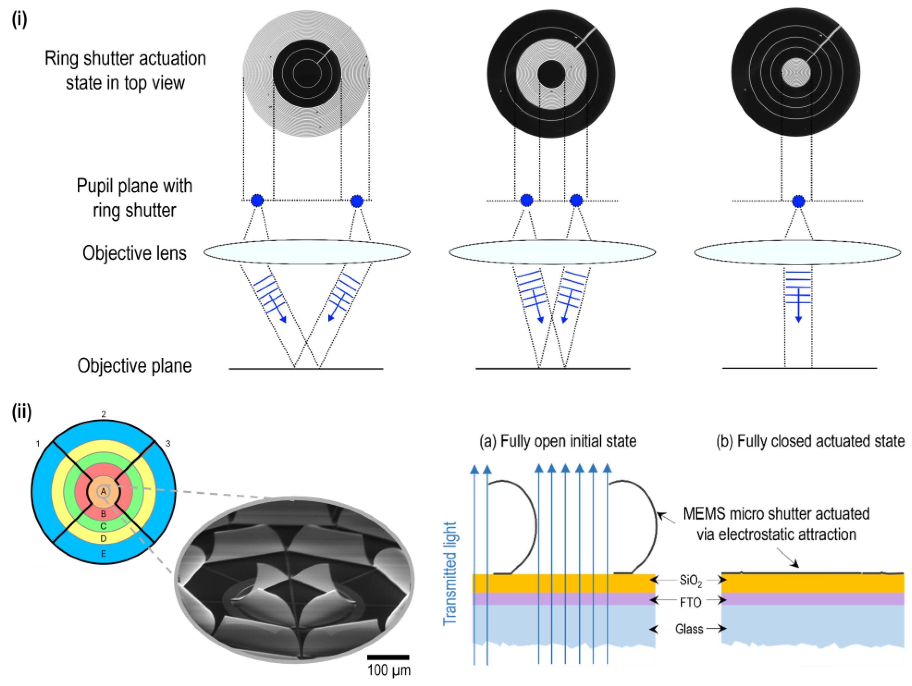
1. Introduction
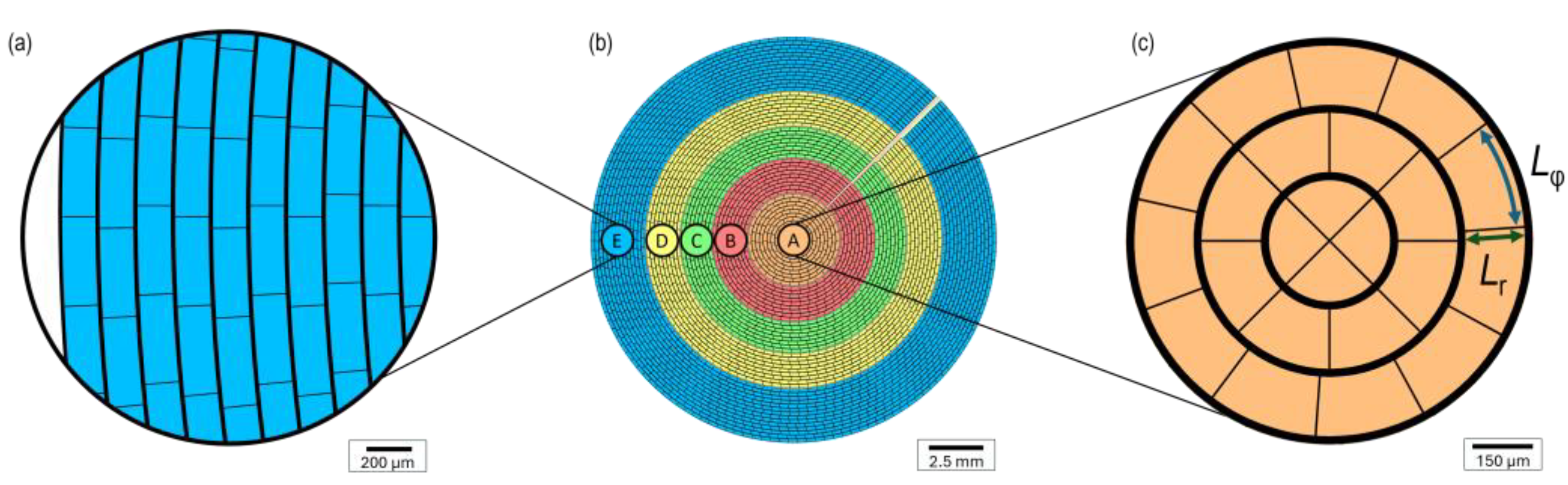
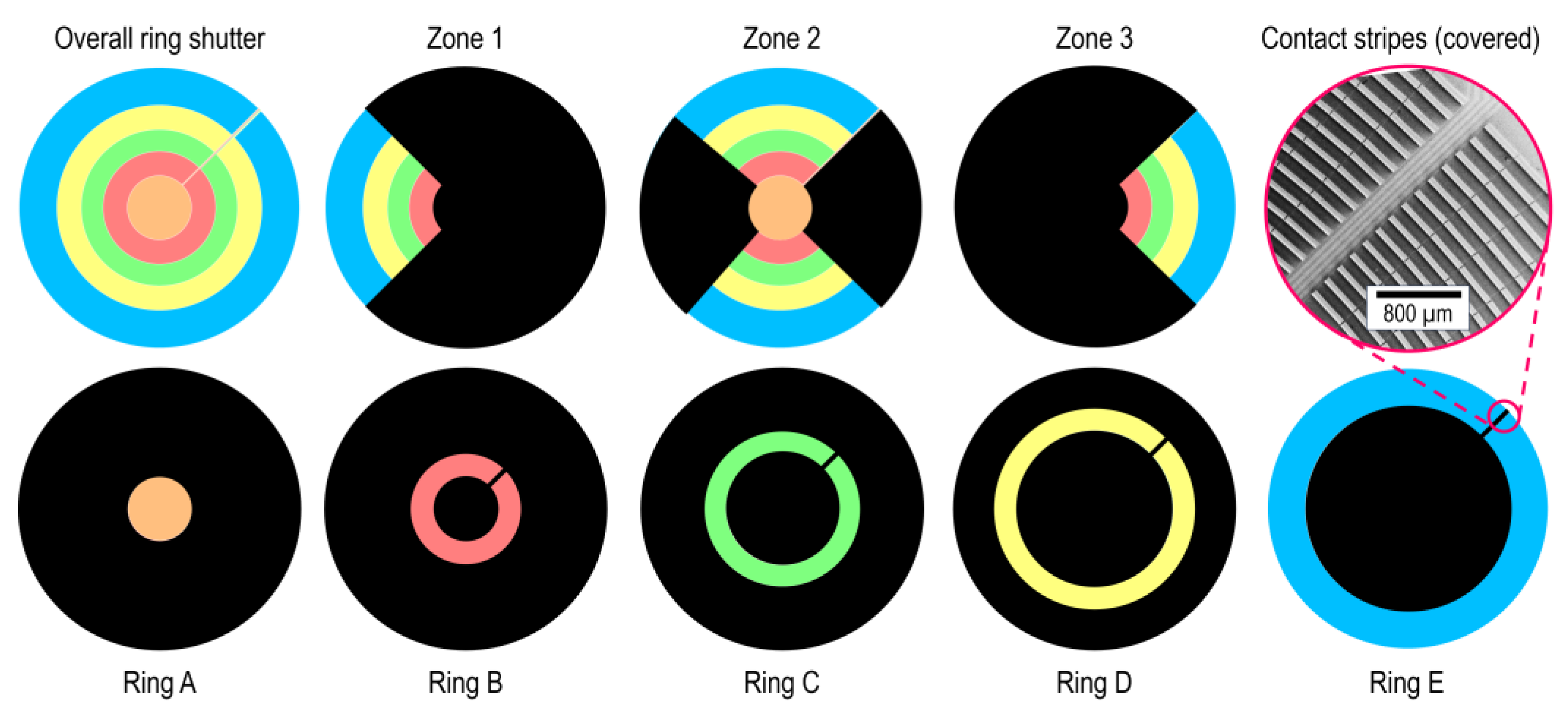
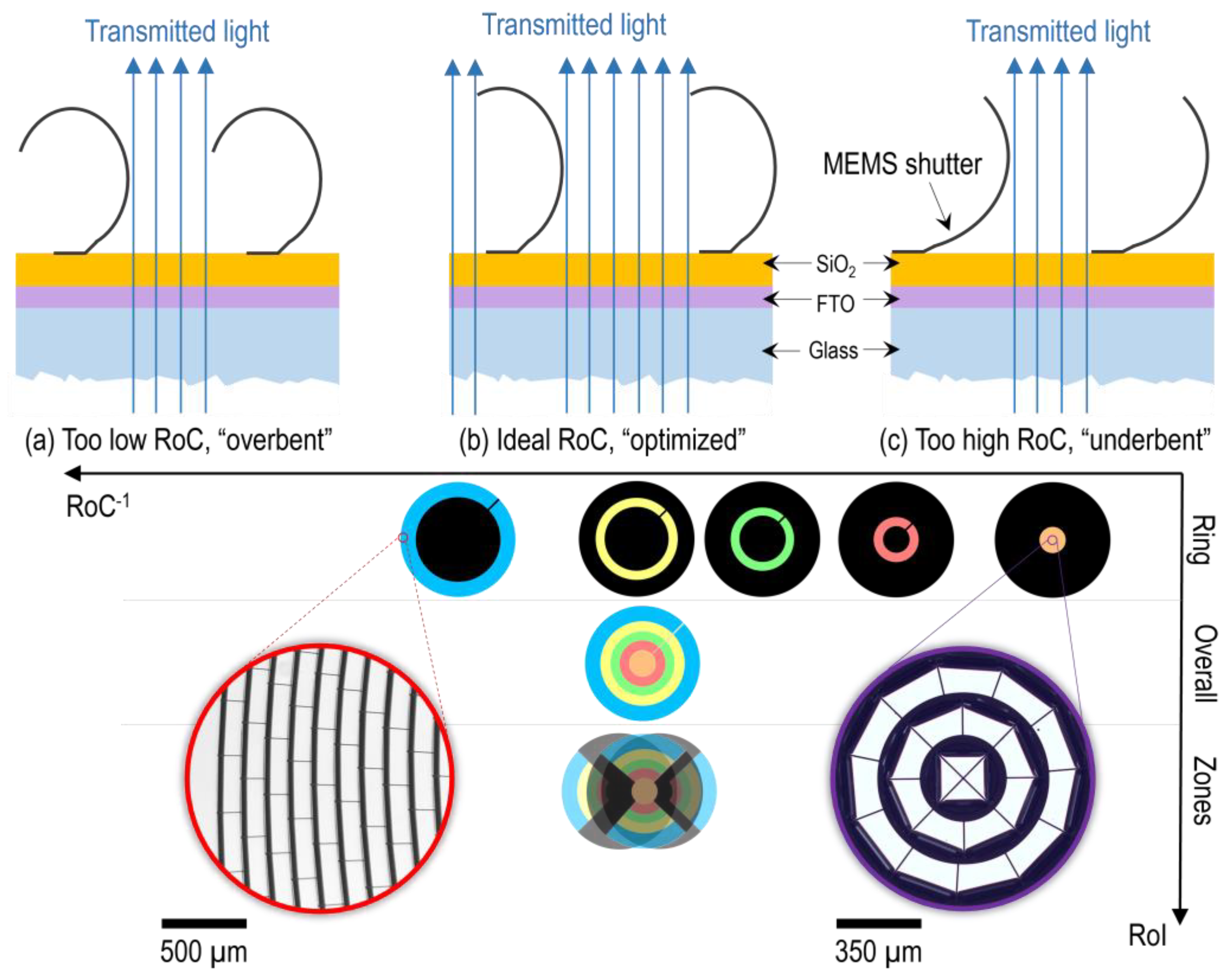
2. Materials and Methods
2.1. Fabrication Process
2.2. Methodology of Characterization
3. Results and Discussion
- Transmission in the initial fully open state for control of optimized stress-induced curling.
- Transmittance-voltage (T-V) curve for determination of actuation voltage and prevention of crosstalk.
- Response dynamics (closing and reopening speed) for targeted high frequency applications.
3.1. Transmission in the Initial Fully Open State
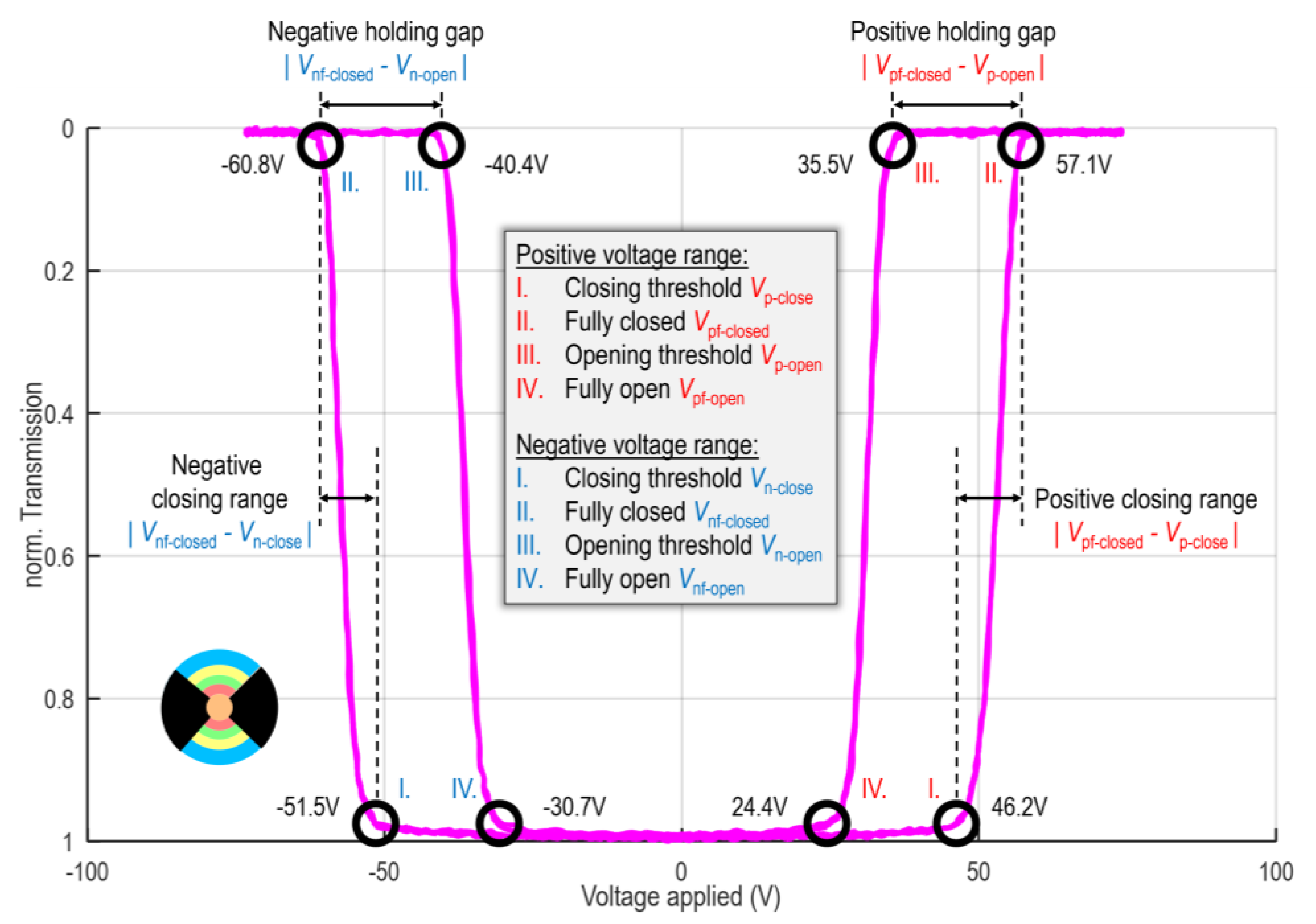
3.2. Transmittance-Voltage (T-V) Curve
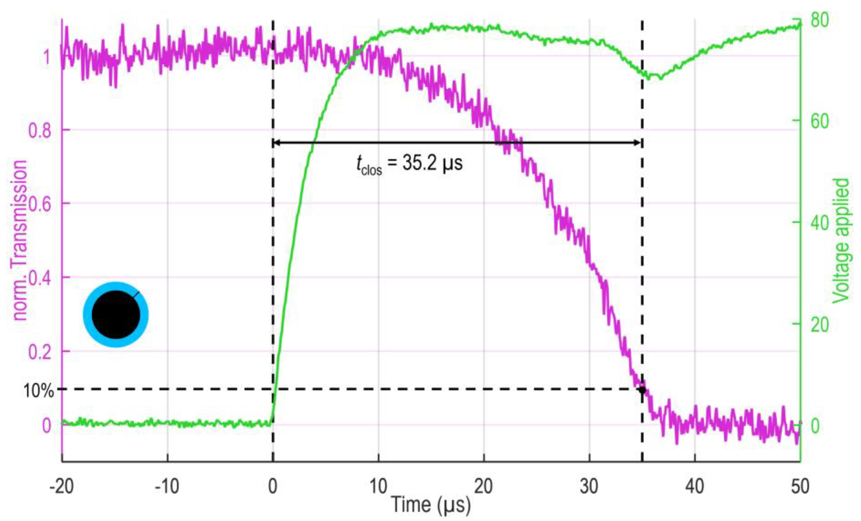
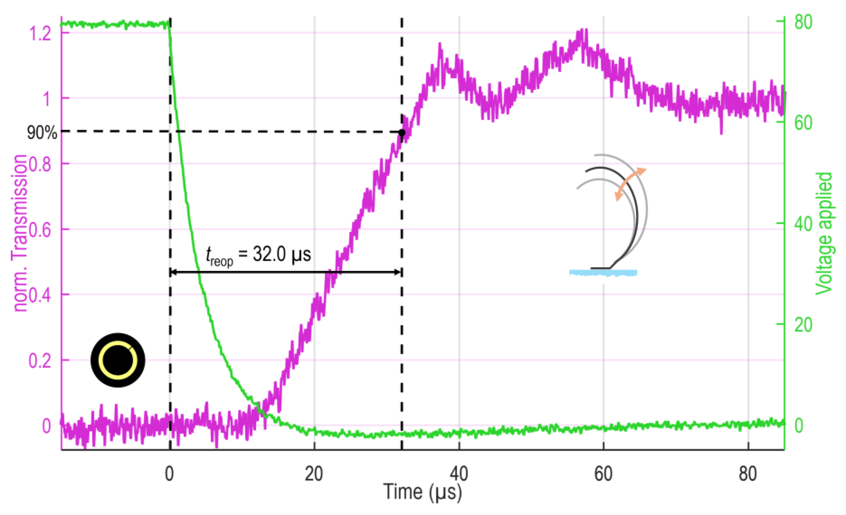
3.3. Response Dynamics (Closing and Reopening Speed)
4. Conclusions
5. Patent
Author Contributions
Funding
Data Availability Statement
Acknowledgments
Conflicts of Interest
References
- Draheim, J.; Burger, T.; Korvink, J.G.; Wallrabe, U. Variable Aperture Stop Based on the Design of a Single Chamber Silicone Membrane Lens with Integrated Actuation. Opt. Lett. 2011, 36, 2032–2034. [Google Scholar] [CrossRef]
- Murade, C.U.; Oh, J.M.; van den Ende, D.; Mugele, F. Electrowetting Driven Optical Switch and Tunable. Opt. Express 2011, 19, 15525–15531. [Google Scholar] [CrossRef] [PubMed]
- Muller, P.; Feuerstein, R.; Zappe, H. Integrated Optofluidic Iris. J. Microelectromech. Syst. 2012, 21, 1156–1164. [Google Scholar] [CrossRef]
- Hein, A.; Kaiser, B.; Kortz, C.; Oesterschulze, E. Tunable Electrochromic Filter for in Situ Fourier Spatial Frequency Filtering. Opt. Express 2021, 29, 7858–7865. [Google Scholar] [CrossRef]
- Schuhladen, S.; Preller, F.; Rix, R.; Petsch, S.; Zentel, R.; Zappe, H. Iris-like Tunable Aperture Employing Liquid-Crystal Elastomers. Adv. Mater. 2014, 26, 7247–7251. [Google Scholar] [CrossRef] [PubMed]
- Zeng, H.; Wani, O.M.; Wasylczyk, P.; Kaczmarek, R.; Priimagi, A. Self-Regulating Iris Based on Light-Actuated Liquid Crystal Elastomer. Adv. Mater. 2017, 29, 1701814. [Google Scholar] [CrossRef]
- Kim, C.-H.; Jung, K.-D.; Kim, W. A wafer-level micro mechanical global shutter for a micro camera. In Proceedings of the 22nd IEEE International Conference on Micro Electro Mechanical Systems, Sorrento, Italy, 25–29 January 2009. [Google Scholar]
- Kästner, P.; Elsaka, B.; Donatiello, R.; Hillmer, H. Ring-Shaped MEMS Shutter Array with Subfield Addressing for Interference Microscopy: Proof of concept. Comms. Eng. 2024; under review. [Google Scholar]
- Künne, M.; Stelter, A.; Pahl, T.; Lehmann, P. Frequency Selective Illumination for High Aperture Coherence Scanning Interferometry. Meas. Sci. Technol. 2024, 35, 115025. [Google Scholar] [CrossRef]
- Liu, S.; Kästner, P.; Donatiello, R.; Shrivastava, A.; Smolarczyk, M.; Iskhandar, M.S.Q.; Hasan, M.K.; Caruso, G.; Chen, J.; Elsaka, B.; et al. State-of-the-Art Materials Used in MEMS Micromirror Arrays for Photonic Applications. Photonics 2024, 11, 253. [Google Scholar] [CrossRef]
- Kästner, P.; Ur Rehman, H.; Donatiello, R.; Elsaka, B.; Hasan, M.K.; Hillmer, H. Ring-Shaped MEMS Shutter Arrays for Interference Microscopy: Designs, Fabrication, Characterization. In Proceedings of the 2024 International Conference on Optical MEMS and Nanophotonics (OMN), San Sebastian, Spain, 28 July–1 August 2024; pp. 1–2. [Google Scholar]
- Yang, X.; Kästner, P.; Käkel, E.; Smolarczyk, M.; Liu, S.; Li, Q.; Hillmer, H. Study of Dynamics in Metallic MEMS Cantilevers—Pull-In Voltage and Actuation Speed. Appl. Sci. 2023, 13, 1118. [Google Scholar] [CrossRef]
- Iskhandar, M.S.Q. Development of Selectively Actuatable Micromirror Arrays and Scalable Lithography. Ph.D. Thesis, University Kassel, Kassel, Germany, 2022. [Google Scholar]
- Elsaka, B.; Kästner, P.; Käkel, E.; Donatiello, R.; Hillmer, H. Investigation of the Influence of Sublayer Thickness on Pairing of Metallic MEMS Shutter Blades. Appl. Sci. 2023, 13, 1538. [Google Scholar] [CrossRef]


| Measure | Overall | Ring A | Ring B | Ring C | Ring D | Ring E | Zone 1 | Zone 2 | Zone 3 |
|---|---|---|---|---|---|---|---|---|---|
| Transmission in % | 53.6 | 44.5 | 49.4 | 51.9 | 53.9 | 58.1 | 54.3 | 53.4 | 52.9 |
| Relative deviation in % | 0 (Ref.) | −17.0 | −7.9 | −3.1 | 0.6 | 8.3 | 1.3 | −0.4 | −1.3 |
| Measure|Evaluation | Overall | Ring A | Ring B | Ring C | Ring D | Ring E | Zone 1 | Zone 2 | Zone 3 |
|---|---|---|---|---|---|---|---|---|---|
| Closing threshold in V | +46.5 −51.7 | +46.5 −51.3 | +46.8 −51.8 | +49.1 −52.8 | +49.3 −51.0 | +49.9 −53.2 | +47.2 −53.5 | +46.2 −51.5 | +46.1 −51.6 |
| Fully closed in V | +56.0 −61.3 | +55.8 −61.6 | +54.6 −62.4 | +59.1 −63.5 | +59.1 −62.2 | +60.2 −62.9 | +57.7 −63.0 | +57.1 −60.8 | +54.4 −59.6 |
| Opening threshold in V | +32.9 −39.0 | +32.0 −39.4 | +33.1 −38.4 | +33.7 −38.5 | +34.8 −38.2 | +34.8 −38.2 | +33.8 −40.4 | +35.5 −40.4 | +32.9 −40.2 |
| Fully open in V | +25.9 −32.4 | +23.6 −30.1 | +26.2 −31.0 | +26.9 −30.1 | +27.6 −29.7 | +27.4 −30.8 | +25.3 −32.5 | +24.4 −30.7 | +25.9 −31.9 |
| Closing range in V | 9.5 9.6 | 9.3 10.3 | 7.8 10.6 | 10.0 10.7 | 10.7 11.2 | 10.3 9.7 | 10.5 9.5 | 10.9 9.3 | 8.3 8.0 |
| Deviation in closing threshold in V|% | 0|0 0|0 | 0.0|0.0 −0.4|−0.8 | 0.3|0.7 0.1|0.2 | 2.6|5.6 1.1|2.1 | 2.8|6.0 −0.7|−1.4 | 3.4|7.3 1.5|2.9 | 0.7|1.5 1.8|3.5 | −0.3|−0.7 −0.2|−0.4 | −0.4|−0.9 −0.1|−0.2 |
| Holding gap in V | 23.1 22.3 | 23.8 22.2 | 21.5 24.0 | 25.4 25.0 | 25.3 25.2 | 25.4 24.7 | 23.9 22.6 | 21.6 20.4 | 21.5 19.4 |
| Response Time | Overall | Ring A | Ring B | Ring C | Ring D | Ring E | Zone 1 | Zone 2 | Zone 3 |
|---|---|---|---|---|---|---|---|---|---|
| Closing in µs | 31.7 | 26.4 | 28.5 | 30.3 | 33.0 | 35.2 | 31.9 | 31.6 | 33.9 |
| Opening in µs | 39.3 | 34.3 | 31.5 | 31.6 | 32.0 | 37.6 | 36.8 | 38.3 | 36.9 |
Disclaimer/Publisher’s Note: The statements, opinions and data contained in all publications are solely those of the individual author(s) and contributor(s) and not of MDPI and/or the editor(s). MDPI and/or the editor(s) disclaim responsibility for any injury to people or property resulting from any ideas, methods, instructions or products referred to in the content. |
© 2025 by the authors. Licensee MDPI, Basel, Switzerland. This article is an open access article distributed under the terms and conditions of the Creative Commons Attribution (CC BY) license (https://creativecommons.org/licenses/by/4.0/).
Share and Cite
Kästner, P.; Elsaka, B.; Iskhandar, M.S.Q.; Liebermann, S.; Donatiello, R.; Liu, S.; Hillmer, H. Homogeneity of Electro-Mechanical and Optical Characteristics in Ring-Shaped MEMS Shutter Arrays with Subfield Addressing for Interference Microscopy. Micromachines 2025, 16, 168. https://doi.org/10.3390/mi16020168
Kästner P, Elsaka B, Iskhandar MSQ, Liebermann S, Donatiello R, Liu S, Hillmer H. Homogeneity of Electro-Mechanical and Optical Characteristics in Ring-Shaped MEMS Shutter Arrays with Subfield Addressing for Interference Microscopy. Micromachines. 2025; 16(2):168. https://doi.org/10.3390/mi16020168
Chicago/Turabian StyleKästner, Philipp, Basma Elsaka, Mustaqim Siddi Que Iskhandar, Steffen Liebermann, Roland Donatiello, Shujie Liu, and Hartmut Hillmer. 2025. "Homogeneity of Electro-Mechanical and Optical Characteristics in Ring-Shaped MEMS Shutter Arrays with Subfield Addressing for Interference Microscopy" Micromachines 16, no. 2: 168. https://doi.org/10.3390/mi16020168
APA StyleKästner, P., Elsaka, B., Iskhandar, M. S. Q., Liebermann, S., Donatiello, R., Liu, S., & Hillmer, H. (2025). Homogeneity of Electro-Mechanical and Optical Characteristics in Ring-Shaped MEMS Shutter Arrays with Subfield Addressing for Interference Microscopy. Micromachines, 16(2), 168. https://doi.org/10.3390/mi16020168