
Capacitance–Voltage Studies on Electrostatically Actuated MEMS Micromirror Arrays †

 , ,
, ,
Abstract
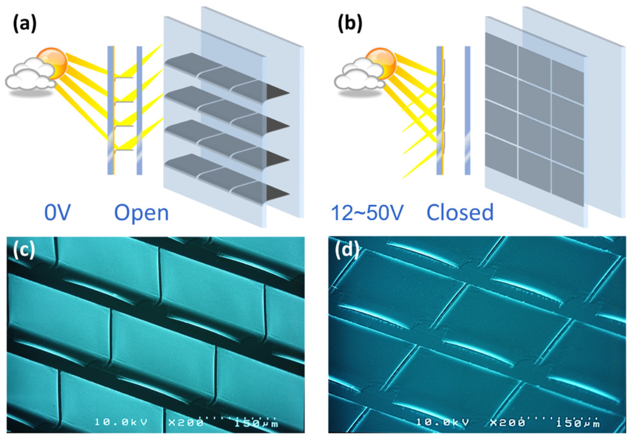
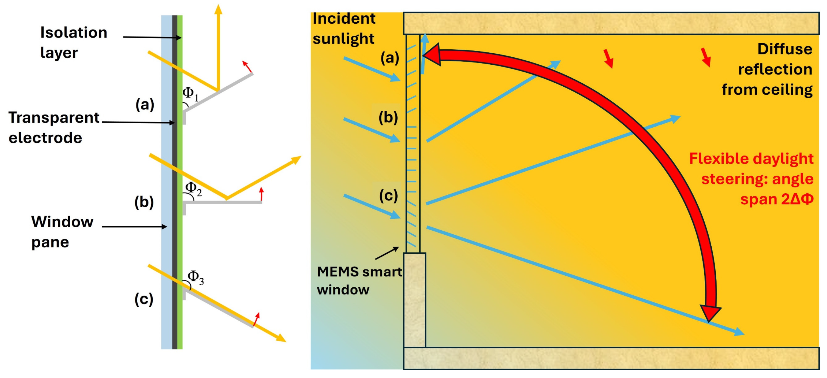
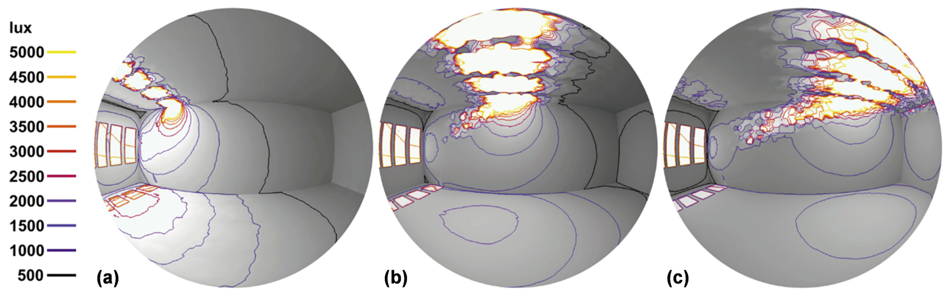
1. Introduction
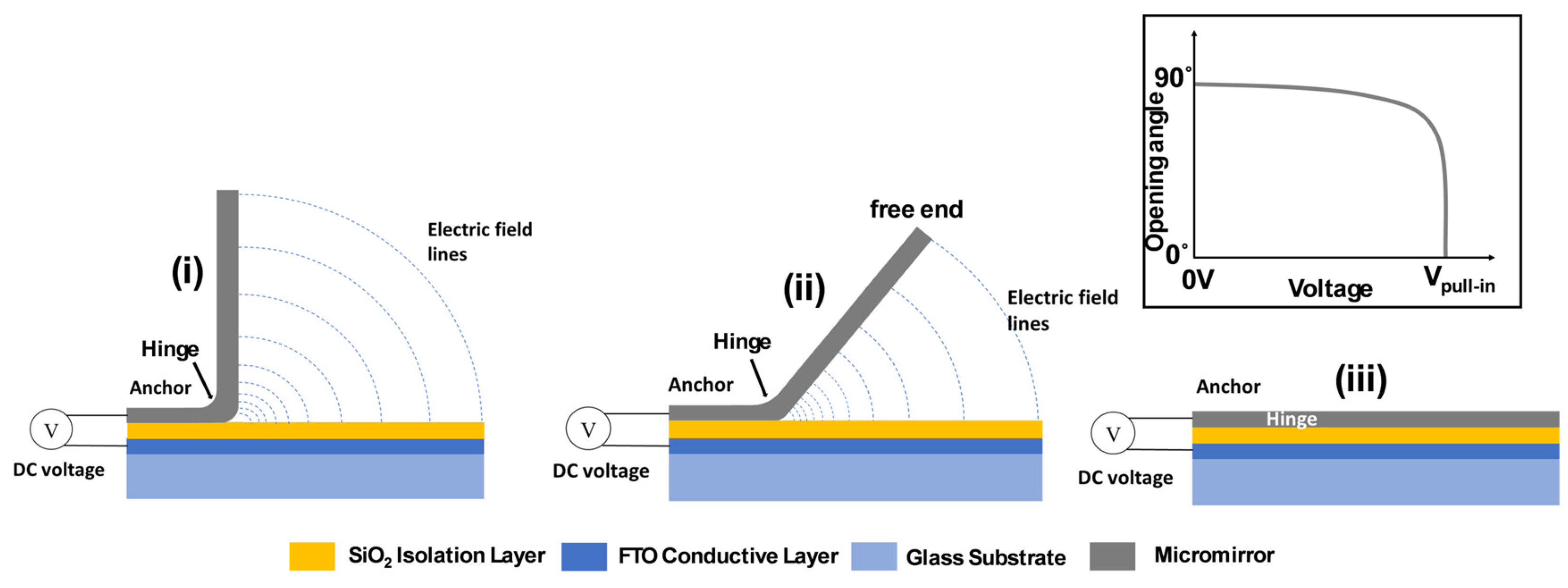
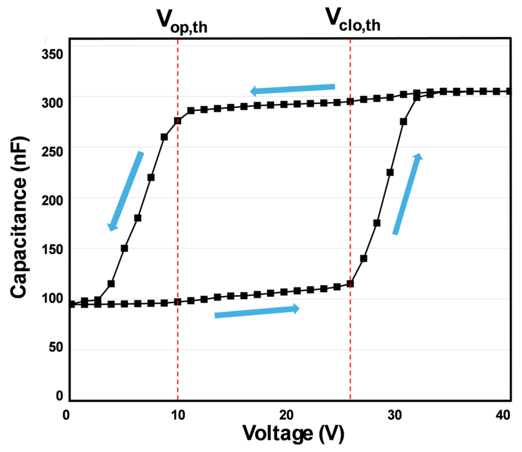
2. Principle of Electrostatic Actuation of Micromirror and CV Study
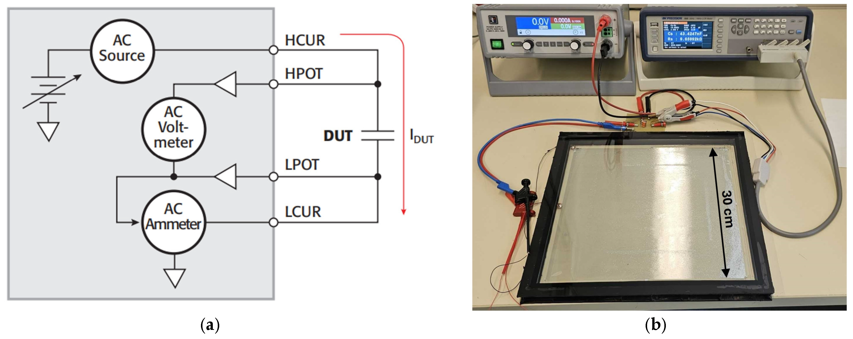
3. Capacitance–Voltage (C-V) Measurement Setups
4. Capacitance–Voltage (C-V) Measurement Results
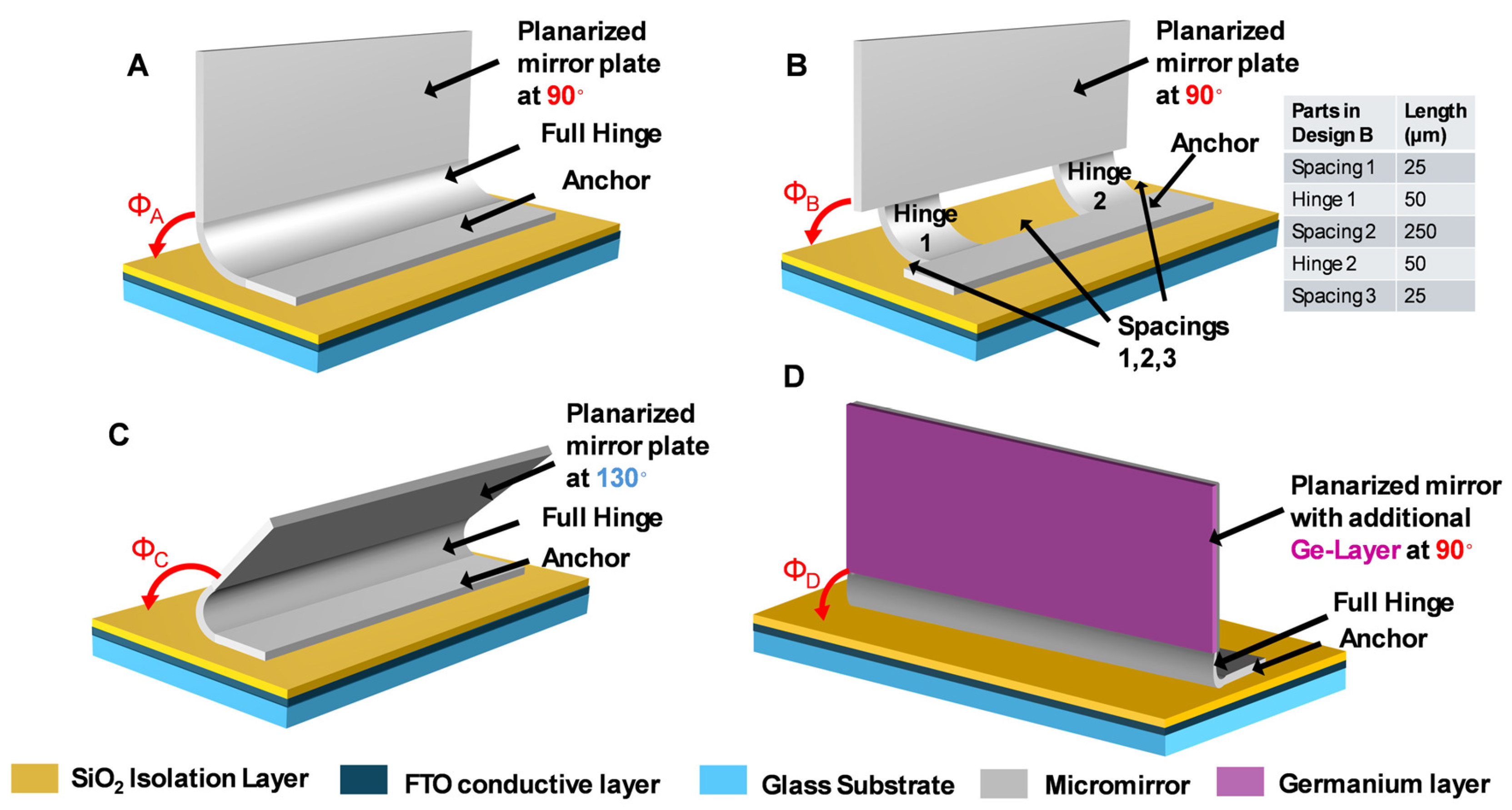
4.1. Technological Fabrication and Introduction of the Four Designs Used in the Experiments
4.2. C-V Measurement Results
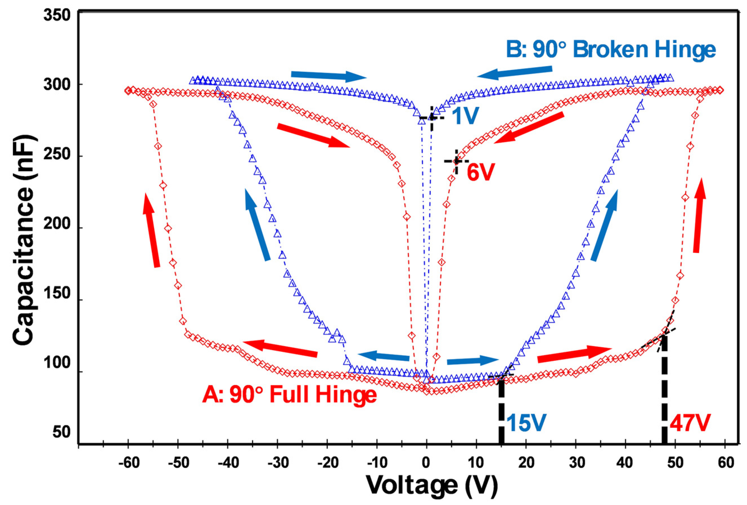
4.2.1. Comparison of Micromirror Designs A and B
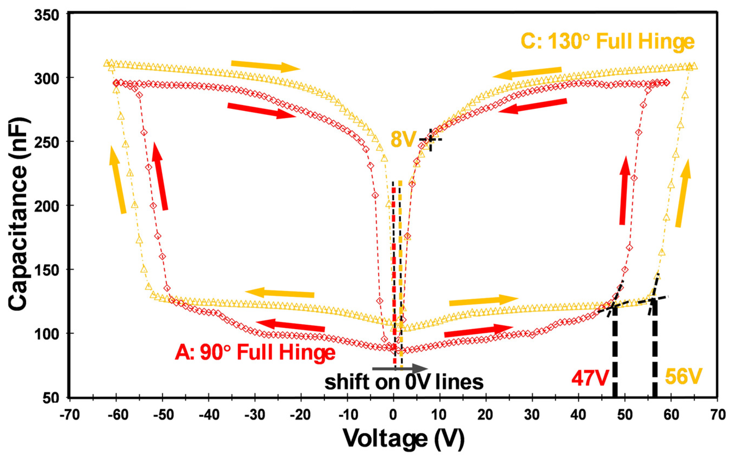
4.2.2. Comparison of Micromirror Designs A and C
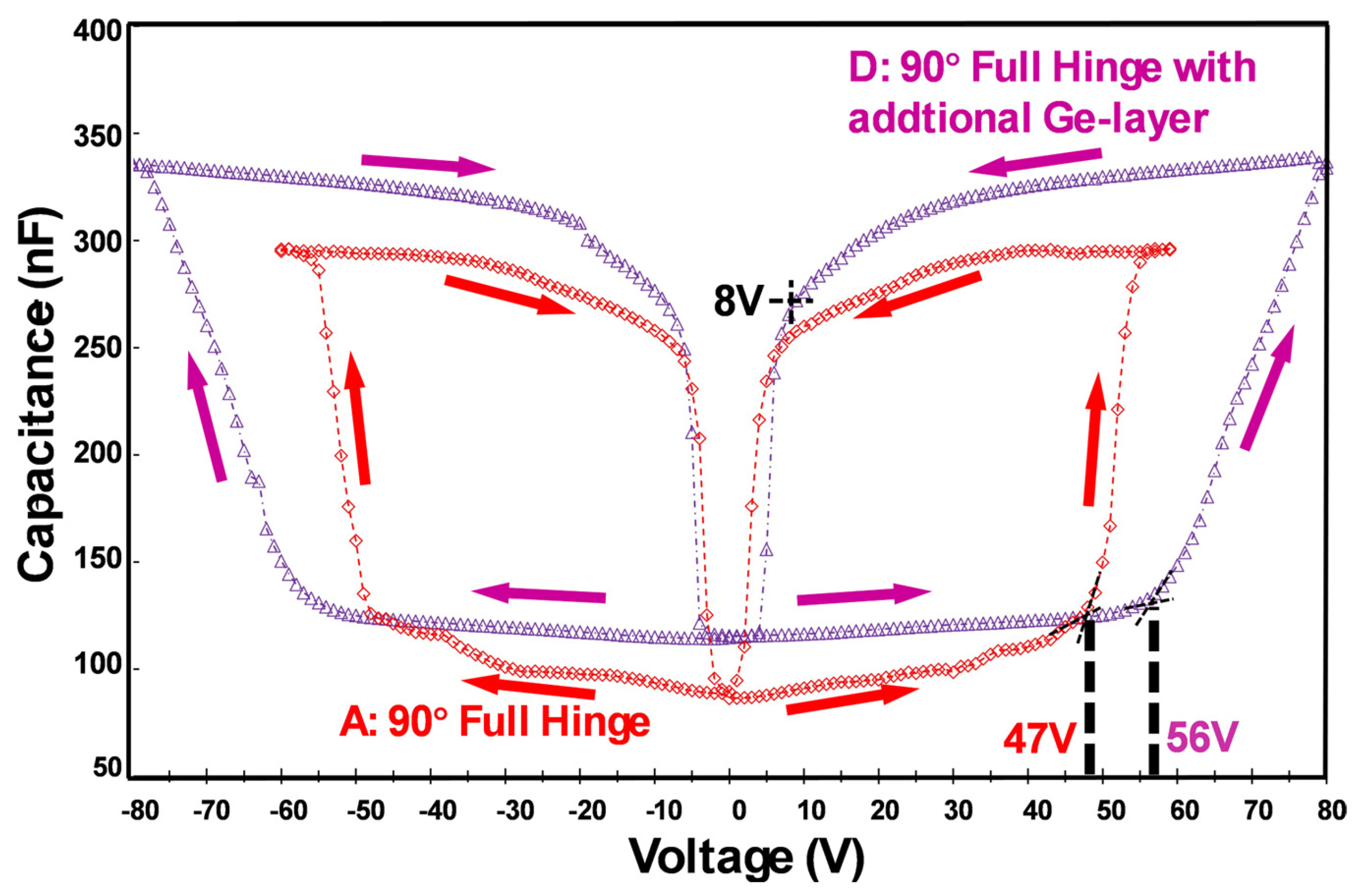
4.2.3. Comparison of Micromirror Designs A and D
5. Conclusions and Outlook
6. Patents
Supplementary Materials
Author Contributions
Funding
Data Availability Statement
Acknowledgments
Conflicts of Interest
References
- Liu, T.; Chen, L.; Yang, M.; Sandanayake, M.; Miao, P.; Shi, Y.; Yap, P.-S. Sustainability Considerations of Green Buildings: A Detailed Overview on Current Advancements and Future Considerations. Sustainability 2022, 14, 14393. [Google Scholar] [CrossRef]
- Mori, K.; Misawa, K.; Ihida, S.; Takahashi, T.; Fujita, H.; Toshiyoshi, H. Electrostatic roll-up blind array for house energy management systems. In 2015 International Conference on Optical MEMS and Nanophotonics (OMN), Jerusalem, Israel, 2–5 August 2015; IEEE: Piscataway, NJ, USA, 2015; pp. 1–2. ISBN 978-1-4673-6834-6. [Google Scholar]
- Mori, K.; Misawa, K.; Ihida, S.; Takahashi, T.; Fujita, H.; Toshiyoshi, H. A MEMS Electrostatic Roll-Up Window Shade Array for House Energy Management System. IEEE Photon. Technol. Lett. 2016, 28, 593–596. [Google Scholar] [CrossRef]
- Bao, S.; Zhang, X.; Jin, P.; Yoshimura, K. Optical properties and switching durability of TiO2 top-coated magnesium–nickel thin-film switchable mirrors. Jpn. J. Appl. Phys. 2015, 54, 45501. [Google Scholar] [CrossRef]
- Hillmer, H.; Al-Qargholi, B.; Khan, M.M.; Worapattrakul, N.; Wilke, H.; Woidt, C.; Tatzel, A. Optical MEMS-based micromirror arrays for active light steering in smart windows. Jpn. J. Appl. Phys. 2018, 57, 08PA07. [Google Scholar] [CrossRef]
- Hillmer, H.H.; Iskhandar, M.S.Q.; Hasan, M.K.; Akhundzada, S.; Al-Qargholi, B.; Tatzel, A. MOEMS micromirror arrays in smart windows for daylight steering. J. Opt. Microsyst. 2021, 1, 014502. [Google Scholar] [CrossRef]
- Balaras, C.A.; Droutsa, K.; Dascalaki, E.; Kontoyiannidis, S. Deterioration of European apartment buildings. Energy Build. 2005, 37, 515–527. [Google Scholar] [CrossRef]
- Sandberg, N.H.; Sartori, I.; Heidrich, O.; Dawson, R.; Dascalaki, E.; Dimitriou, S.; Vimm-r, T.; Filippidou, F.; Stegnar, G.; Šijanec Zavrl, M.; et al. Dynamic building stock modelling: Application to 11 European countries to support the energy efficiency and retrofit ambitions of the EU. Energy Build. 2016, 132, 26–38. [Google Scholar] [CrossRef]
- Worapattrakul, N. Micromirrors for Daylight Steering Applications; Kassel University Press: Kassel, Germany, 2017. [Google Scholar]
- Hasan, M.K.; Baby, S.; Muringakodan, S.; Nandakumar, A.; Iskhandar, M.; Hillmer, V.; Li, Q.; Xu, G.; Hillmer, H. Energy Saving and Amortization Time Simulation for a Model Room with MEMS Smart Glazing. In Surface Technology Yearbook; Leuze Verlag: Bad Saulgau, Germany, 2021; ISBN 978-3-87480-369-4. [Google Scholar]
- Aksyuk, V.A.; Pardo, F.; Carr, D.; Greywall, D.; Chan, H.B.; Simon, M.E.; Gasparyan, A.; Shea, H.; Lifton, V.; Bolle, C.; et al. Beam-steering micromirrors for large optical cross-connects. J. Light. Technol. 2003, 21, 634–642. [Google Scholar] [CrossRef]
- Doble, N.; Williams, D.R. The Application of MEMS Technology for Adaptive Optics in Vision Science. IEEE J. Select. Top. Quantum Electron. 2004, 10, 629–635. [Google Scholar] [CrossRef]
- Ballard, B.; Bhakta, V.; Douglass, M.; Gelabert, P.; Kempf, J.; McDonald, W.; Pettitt, G.; Rancuret, P.; Rankin, A.; Thompson, J.; et al. 5-1: Invited Paper: ‘Steering’ Light with Texas Instruments Digital Micromirror Device (DMD)—Past, Present & Future. SID Symp. Dig. Tech. Pap. 2016, 47, 28–31. [Google Scholar] [CrossRef]
- Chen, J.; Yang, X.; Hasan, M.K.; Iskhandar, M.S.Q.; Donatiello, R.; Hillmer, H. Micromirror Arrays for Light Steering Smart Window Applications: Achieving Larger Spans of Opening Angles. In Proceedings of the 2024 International Conference on Optical MEMS and Nanophotonics (OMN), San Sebastian, Spain, 28 July–1 August 2024; IEEE: Piscataway, NJ, USA, 2024; pp. 1–2, ISBN 979-8-3503-8492-5. [Google Scholar]
- Hasan, M.K.; Iskhandar, M.S.Q.; Juvale, S.N.; Baby, S.; Chen, J.; Hillmer, H. Overcoming Pull-in Limitations of Optical MEMS Based Micromirror Arrays Using Structured Bottom Electrodes. In Proceedings of the 2024 International Conference on Optical MEMS and Nanophotonics (OMN), San Sebastian, Spain, 28 July–1 August 2024; IEEE: Piscataway, NJ, USA, 2024; pp. 1–2, ISBN 979-8-3503-8492-5. [Google Scholar]
- Yang, X.; Chen, J.; Iskhandar, M.S.Q.; Qasim, M.H.; Xu, G.; Hillmer, H. Investigation on Bistable Closing Behaviors of Metallic MOEMS Micromirrors with Various Initial Opening Angles. In Proceedings of the 2024 International Conference on Optical MEMS and Nanophotonics (OMN), San Sebastian, Spain, 28 July–1 August 2024; IEEE: Piscataway, NJ, USA, 2024; pp. 1–2, ISBN 979-8-3503-8492-5. [Google Scholar]
- Iskhandar, M.S.Q.; Luo, H.; Ekaputera, K.A.; Al-Qargholi, B.; Khan, M.M.; Hillmer, H. Design, Fabrication and Characterization of Subfield Addressing in Micromirror Arrays for Smart Window Applications. In Proceedings of the 2019 International Conference on Optical MEMS and Nanophotonics: OMN 2019, KAIST, Daejeon, Republic of Korea, 28 July–1 August 2019; IEEE: Piscataway, NJ, USA, 2019. ISBN 9781728145037. [Google Scholar]
- Hassan, M.K.; Liebermann, S.; Iskhandar, M.S.Q.; Löber, D.; Li, Q.; Xu, G.; Hillmer, H. Personalized Light Steering in Buildings Utilizing 2D Actuation in MEMS Micromirror Arrays. In Jahrbuch Oberflächentechnik; Leuze Verlag: Bad Saulgau, Germany, 2022; pp. 217–237. [Google Scholar]
- Ahmad, M.; Bahri, M.; Sawan, M. MEMS Micromirror Actuation Techniques: A Comprehensive Review of Trends, Innovations, and Future Prospects. Micromachines 2024, 15, 1233. [Google Scholar] [CrossRef] [PubMed]
- Tang, Y.; Li, J.; Xu, L.; Lee, J.-B.; Xie, H. Review of Electrothermal Micromirrors. Micromachines 2022, 13, 429. [Google Scholar] [CrossRef] [PubMed]
- Xiao, L.; Ding, Y.; Wang, P.; Xie, H. Analog-controlled light microshutters based on electrothermal actuation for smart windows. Opt. Express 2020, 28, 33106–33122. [Google Scholar] [CrossRef]
- Zhao, C.; Zhao, C.Z.; Lu, Q.; Yan, X.; Taylor, S.; Chalker, P.R. Hysteresis in Lanthanide Aluminum Oxides Observed by Fast Pulse CV Measurement. Materials 2014, 7, 6965–6981. [Google Scholar] [CrossRef]
- Lai, C.H.; Wong, W.S.H. Temperature dependent actuation voltage for longer MEMS switch lifetime. In Proceedings of the 2nd Asia Symposium on Quality Electronic Design (ASQED 2010), Penang, Malaysia, 3–4 August 2010; Lai, C.H., Wong, W., Eds.; IEEE: Piscataway, NJ, USA, 2010; pp. 43–48, ISBN 978-1-4244-7809-5. [Google Scholar]
- Walls, J.A. Capacitance-Voltage Measurements: An Expert System Approach. Ph.D. Thesis, University of Edinburgh, Edinburgh, UK, 1990. [Google Scholar]
- Lamontagne, B.; Fong, N.R.; Song, I.-H.; Ma, P.; Barrios, P.; Poitras, D. Review of microshutters for switchable glass. J. Micro/Nanolith. MEMS MOEMS 2019, 18, 040901. [Google Scholar] [CrossRef]
- Chiu, F.-C. A Review on Conduction Mechanisms in Dielectric Films. Adv. Mater. Sci. Eng. 2014, 2014, 578168. [Google Scholar] [CrossRef]
- Gong, C.; Mehrl, D. Characterization of the Digital Micromirror Devices. IEEE Trans. Electron. Devices 2014, 61, 4210–4215. [Google Scholar] [CrossRef]
- van Spengen, W.M.; Czarnecki, P.; Poets, R.; van Beek, J.; de Wolf, I. The influence of the package environment on the functioning and reliability of RF-MEMS switches. In Proceedings of the 2005 IEEE International Reliability Physics Symposium, 2005. Proceedings. 43rd Annual, San Jose, CA, USA, 17–21 April 2005; IEEE: Piscataway, NJ, USA, 2005; pp. 337–341, ISBN 0-7803-8803-8. [Google Scholar]
- Stauffer, L. CV Measurement Tips, Tricks, and Traps; Keithley: Cleveland, OH, USA, 2011. [Google Scholar]
- Cristea, M.J. Capacitance-voltage profiling techniques for characterization of semiconductor materials and devices. arXiv 2010, arXiv:1011.3463. [Google Scholar]
- Tian, W.; Li, P.; Yuan, L. Research and Analysis of MEMS Switches in Different Frequency Bands. Micromachines 2018, 9, 185. [Google Scholar] [CrossRef]
- Midili, V. Realization of a Capacitance-Voltage Measurement System for Semiconductor Characterization. Master’s Thesis, Aalto University, Espoo, Finland, 2012. [Google Scholar]
- Stauffer, L. Fundamentals of semiconductor CV measurements. EE Eval. Eng. 2008, 47, 20–24. [Google Scholar]
- Zhu, Y.; Espinosa, H.D. Effect of temperature on capacitive RF MEMS switch performance—A coupled-field analysis. J. Micromech. Microeng. 2004, 14, 1270–1279. [Google Scholar]
- Qasim, M.H.; Chen, J.; Iskhandar, M.S.Q.; Hasan, M.K.; Baby, S.; Elsaka, B.; Löber, D.; Xu, G.; Hillmer, H. Advancements in Surface Modification and Coloring Technologies for MEMS-Based Smart Windows: Ultra-Thin Highly Absorbing Films and C-V Measurements of Smart Glass as Sustainable Energy Solutions. In Jahrbuch Oberflächentechnik; Eugen, G., Ed.; Leuze Verlag: Bad Saulgau, Germany, 2023; ISBN 9783874803861. [Google Scholar]
- Liu, S.; Kästner, P.; Donatiello, R.; Shrivastava, A.; Smolarczyk, M.; Iskhandar, M.S.Q.; Hasan, M.K.; Caruso, G.; Chen, J.; Elsaka, B.; et al. State-of-the-Art Materials Used in MEMS Micromirror Arrays for Photonic Applications. Photonics 2024, 11, 253. [Google Scholar] [CrossRef]
- Khudhair, B.; Viereck, V.; Hillmer, H. Microstructure and method of producing a microstructure in a photolithography technique. DE102015117556A1, 20 April 2017. [Google Scholar]
- Yang, X. Theoretical Analyses and Simulations of Characteristics of MOEMS Microelement Arrays for Daylight Steering; Kassel University Press: Kassel, Germany, 2024. [Google Scholar]
- Nielson, G.N.; Barbastathis, G. Dynamic Pull-In of Parallel-Plate and Torsional Electrostatic MEMS Actuators. J. Microelectromech. Syst. 2006, 15, 811–821. [Google Scholar] [CrossRef]
- Zhang, W.-M.; Yan, H.; Peng, Z.-K.; Meng, G. Electrostatic pull-in instability in MEMS/NEMS: A review. Sens. Actuators A Phys. 2014, 214, 187–218. [Google Scholar] [CrossRef]
- Papaioannou, G.J.; Lisec, T. 2007 European Microwave Integrated Circuits Conference. In Proceedings of the European Microwave Integrated Circuits Conference 2007, Munich, Germany, 8–10 October 2007; IEEE Service Center: Piscataway, NJ, USA, 2007. ISBN 2874870021. [Google Scholar]
- Sumant, P.S.; Aluru, N.R.; Cangellaris, A.C. A compact model for dielectric charging in RF MEMS capacitive switches. Int. J. RF Microw. Comp. Aid. Eng. 2009, 19, 197–203. [Google Scholar] [CrossRef]
- Papaioannou, G.J.; Exarchos, M.; Theonas, V.; Psychias, J.; Konstantinidis, G.; Vasilache, D.; Muller, A.; Neculoiu, D. Effect of space charge polarization in radio frequency microelectromechanical system capacitive switch dielectric charging. Appl. Phys. Lett. 2006, 89, 103512. [Google Scholar] [CrossRef]
- Nazemroaya, S.; Iskhandar, M.; Hasan, M.K.; Li, Q.; Hillmer, H. Concepts for clear View through 3D Structured Surfaces o MEMS Smart Glass: Design, Implementation, Characterization and Validation. In Jahrbuch Oberflächentechnik; Leuze Verlag: Bad Saulgau, Germany, 2020; Volume 76, pp. 101–115. ISBN 978-3-87480-364-9. [Google Scholar]
- Iskhandar, M.S.Q.; Al-Qargholi, B.; Khan, M.M.; Tatzel, A.; Luo, H.; Nazemroaya, S.; Li, Q.; Hillmer, H. Development of optical MEMS-based micromirror arrays for smart window applications: Implementation of subfield addressing and reliability measurements. In Jahrbuch Oberflächentechnik; Leuze Verlag: Bad Saulgau, Germany, 2019; Volume 75, pp. 93–107. ISBN 978-3-87480-357-1. [Google Scholar]
- Baby, S.; Iskhandar, M.S.Q.; Hasan, M.K.; Liebermann, S.; Chen, J.; Qasim, H.; Liu, S.; Farrag, E.; Löber, D.; Ahmed, N.; et al. Advancements in MEMS Micromirror and Microshutter Arrays for Light Transmission Through a Substrate. Micromachines 2025, 16, 103. [Google Scholar] [CrossRef]


| Parameters | Setting |
|---|---|
| Measurement mode | Cs (series capacitor) |
| Sweep voltage [V] | −100 to ~100 |
| Stepsize (increment) [V] | 1 |
| Frequency [kHz] | 10 |
| Micromirror array size [cm2] | 100 (10 × 10), etc. |
| Temperature [°C] | 20 |
| Micromirror Array Designs | Material Combinations | Hinge Difference Configurations (Spacing 1 + Hinge 1 + Spacing 2 + Hinge 2 + Spacing 3) | Opening Angle |
|---|---|---|---|
| A | Al, Cr | (0 + 400 + 0 + 0 + 0) μm | ≈90° |
| B | Al, Cr | (25 + 50 + 250 + 50 + 25) μm | ≈90° |
| C | Al, Cr | (0 + 400 + 0 + 0 + 0) μm | ≈130° |
| D | Al, Cr, Ge | (0 + 400 + 0 + 0 + 0) μm | ≈90° |
| Micromirror Array Designs | A | B | C | D |
|---|---|---|---|---|
| Threshold voltage for the closing processes (Vclo,th) | 47 V | 15 V | 56 V | 56 V |
| Threshold voltage for the reopening process (Vop,th) | 6 V | 1 V | 8 V | 8 V |
Disclaimer/Publisher’s Note: The statements, opinions and data contained in all publications are solely those of the individual author(s) and contributor(s) and not of MDPI and/or the editor(s). MDPI and/or the editor(s) disclaim responsibility for any injury to people or property resulting from any ideas, methods, instructions or products referred to in the content. |
© 2025 by the authors. Licensee MDPI, Basel, Switzerland. This article is an open access article distributed under the terms and conditions of the Creative Commons Attribution (CC BY) license (https://creativecommons.org/licenses/by/4.0/).
Share and Cite
Chen, J.; Yang, X.; Iskhandar, M.S.Q.; Hasan, M.K.; Baby, S.; Qasim, M.H.; Löber, D.; Liu, S.; Donatiello, R.; Liebermann, S.; et al. Capacitance–Voltage Studies on Electrostatically Actuated MEMS Micromirror Arrays. Micromachines 2025, 16, 157. https://doi.org/10.3390/mi16020157
Chen J, Yang X, Iskhandar MSQ, Hasan MK, Baby S, Qasim MH, Löber D, Liu S, Donatiello R, Liebermann S, et al. Capacitance–Voltage Studies on Electrostatically Actuated MEMS Micromirror Arrays. Micromachines. 2025; 16(2):157. https://doi.org/10.3390/mi16020157
Chicago/Turabian StyleChen, Jiahao, Xiaohui Yang, Mustaqim Siddi Que Iskhandar, Md. Kamrul Hasan, Shilby Baby, Muhammad Hasnain Qasim, Dennis Löber, Shujie Liu, Roland Donatiello, Steffen Liebermann, and et al. 2025. "Capacitance–Voltage Studies on Electrostatically Actuated MEMS Micromirror Arrays" Micromachines 16, no. 2: 157. https://doi.org/10.3390/mi16020157
APA StyleChen, J., Yang, X., Iskhandar, M. S. Q., Hasan, M. K., Baby, S., Qasim, M. H., Löber, D., Liu, S., Donatiello, R., Liebermann, S., Xu, G., & Hillmer, H. (2025). Capacitance–Voltage Studies on Electrostatically Actuated MEMS Micromirror Arrays. Micromachines, 16(2), 157. https://doi.org/10.3390/mi16020157