3. Results and Discussion
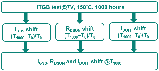
To assess the reliability of the device, a High-Temperature Gate Bias (HTGB) test was conducted under controlled conditions of V
G = 7 V, 150 °C, and 1000 h, as depicted in
Figure 6. The key performance indicators for this test are the shifts in I
GSS (Gate Source Leakage Current), R
DSON (ON Resistance), and I
DSS (Drain Source Leakage Current). As a result, 1 part fails out of 231 testing parts after 96 h of stress.
Figure 7 illustrates the I
D-V
D curve after 96 h of HTGB stress, revealing an increase in drain leakage current, which indicates device failure.
To investigate the cause of failure, decapsulation hot spot analysis is performed. The top metal layer was removed to enhance the likelihood of detecting a hot spot. By sweeping I
DOFF to V
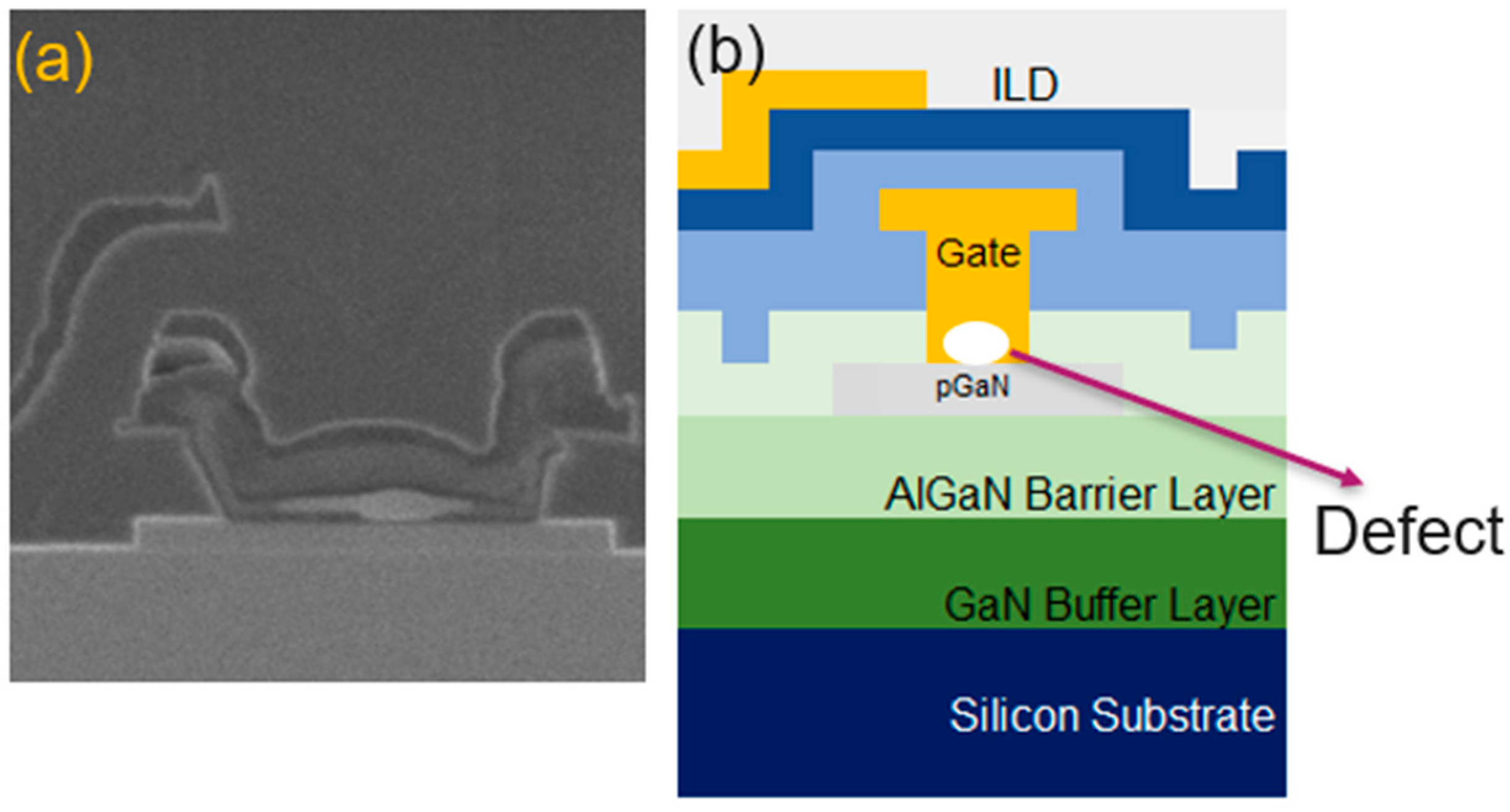
D = 650 V, an InGaAs hot spot was identified, and a cross-sectional analysis was conducted at the hot spot location, as shown in
Figure 8a, to further elucidate the failure mechanism.
The Focused Ion Beam (FIB) cross-section in
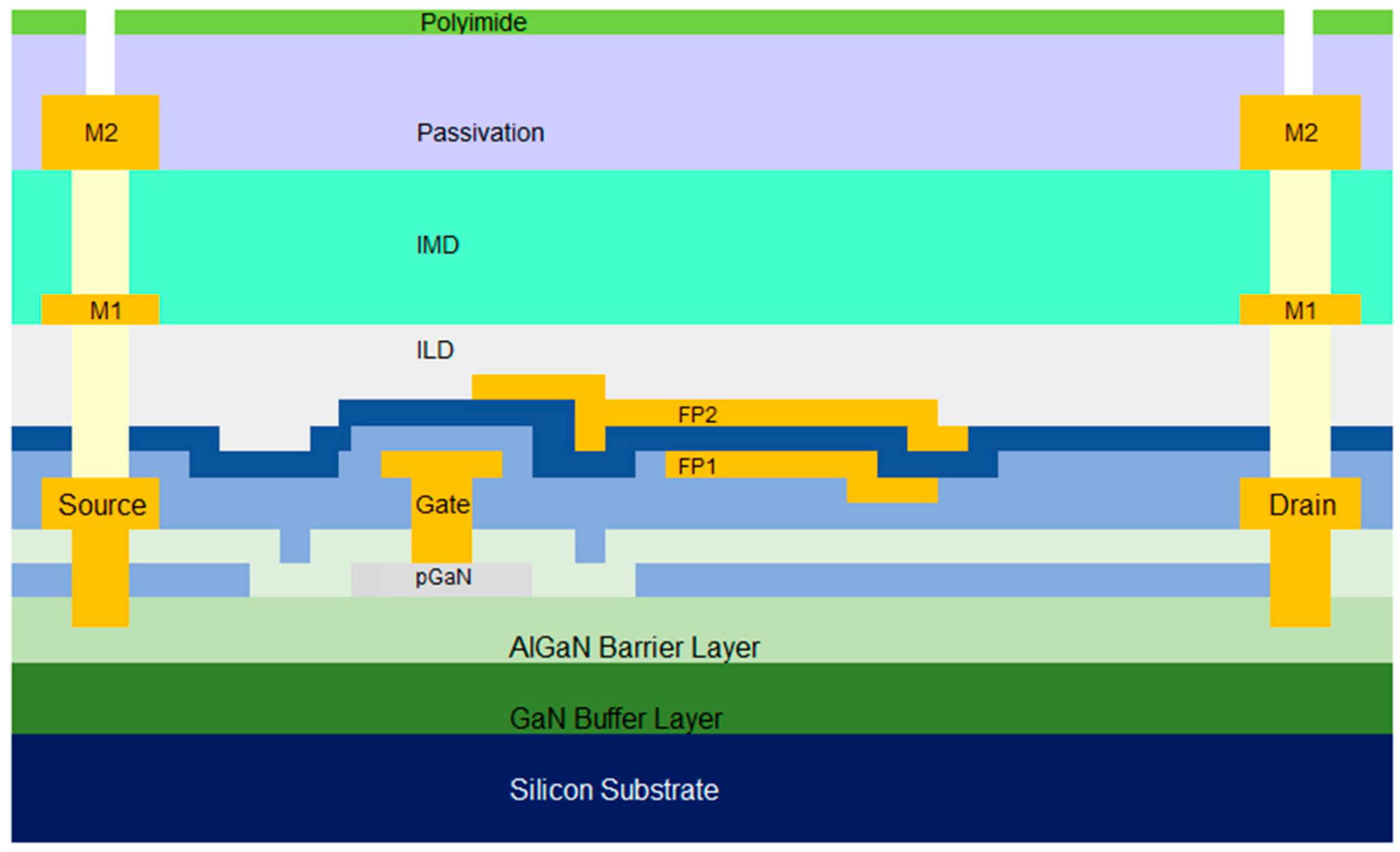
Figure 8a reveals a defect at the bottom of the gate metal, which is identified as a hot spot. A simplified illustration in
Figure 8b helps to clarify the finding, indicating that the defect is located within the gate metal and is attributed to the gate metal deposition process. A detailed material characterization of the observed gate metal defect was performed using Scanning Electron Microscopy with Energy-Dispersive X-ray Spectroscopy (SEM-EDS). The analysis, conducted at an accelerating voltage of 5 keV, confirmed that the elemental composition of the defect site was spectroscopically identical to the surrounding bulk gate metal. This result strongly suggests that the defect volume is below the characteristic X-ray generation volume for the smallest beam energy, which is 5 keV. Specifically, the X-ray interaction volume at 5 keV is significantly larger than the defect itself, causing the resultant spectrum to be dominated by the underlying or surrounding bulk material.
The gate electrode itself features a multi-layer, or “sandwich,” composition, consisting of three distinct metal layers, as
Figure 8a shows. These layers are sequentially deposited within a single, high-vacuum sputtering tool, utilizing separate, dedicated process chambers to ensure purity and control over individual layer properties. Given this integrated, high-vacuum manufacturing flow, introducing an in situ optical scanning or inspection step between the deposition of each metal layer is highly impractical and technically inadvisable. Any such interruption to the vacuum integrity, even for a brief period, would inevitably expose the newly deposited metal surface to ambient conditions, leading to rapid oxidation. This interfacial oxidation, in turn, severely compromises the crucial inter-layer adhesion, potentially creating new, more severe reliability issues.
To mitigate the current defectivity while maintaining process integrity, we have already enhanced the deployment of off-line monitoring and statistical process control (SPC) techniques during the metal deposition sequence. This allows for a more sensitive and rapid detection of incipient defects. However, despite these improvements in process control monitoring, a comprehensive review of the reliability data indicates that more stringent, testing methodologies and preventive measures are critically required across the entire fabrication module. These additional mechanisms are necessary to further suppress the underlying defect generation rate and achieve a substantially reduced, industry-leading long-term device failure rate.
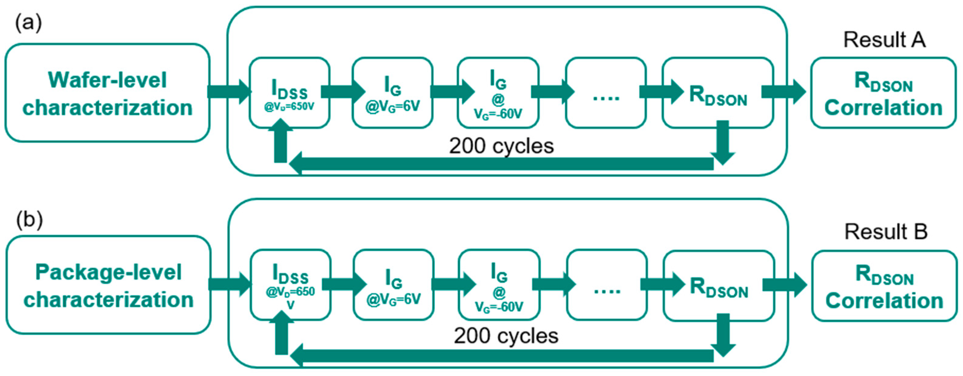
Testing data correlation is deployed. The looping test is our standard wafer-level reliability test for the R
DSON monitor, as shown in
Figure 9. The major items in the loop-run test are I
DSS at V
D = 650 V, V
G at V
G = 6 V, V
G@V
G = −60 V and R
DSON. The loop-run testing items go through 200 cycles and ((R
DSON,T=200 − R
DSON,T=0)/R
DSON,T=0) is calculated for the R
DSON monitor as result A for wafer-level characterization (
Figure 9a). The same loop-run testing items go through 200 cycles and ((R
DSON,T=200 − R
DSON,T=0)/R
DSON,T=0) is calculated for the R
DSON monitor as result B for package-level characterization (
Figure 9b). To screen out the gate metal defect, a loop-run testing data correlation approach is employed and associated with the gate-related testing items, such as V
G = 6 V and V
G = −60 V. As a result, the testing data reveal a correlation with the reverse gate bias test at V
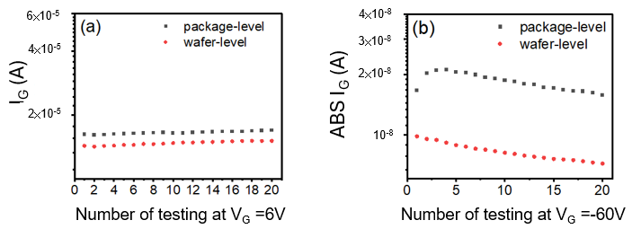
G = −60 V. A series of 20 sequential tests are conducted at both wafer level (Sample A) and package-level (Sample B), with a focus on the changes in I
G at V
G = −60 V between the 1st and 3rd tests, as well as between the 18th and 20th tests, as shown in
Figure 10.
A lack of correlation was observed between the Forward Gate Current (I
GON), measured at a gate voltage (V
G) of 6 V, and the number of subsequent pulse test cycles, for both the wafer-level (Sample A) and package-level (Sample B) specimens, as illustrated in
Figure 11a. This insensitivity is primarily attributed to the inherent high gate leakage current characteristic of these devices. This leakage stems from the relatively small energy barriers present at two critical interfaces: the Two-Dimensional Electron Gas (2DEG)/Aluminum Gallium Nitride (AlGaN) interface and the AlGaN/passivation layer interface. Consequently, the measured Forward Gate Current does not predominantly reflect the electrical state of the gate metal itself, but rather the total leakage current flowing through the passivation and overlying dielectric layers. Therefore, under forward gate bias conditions, the measured I
GON is not a sufficiently sensitive indicator for detecting subtle gate metal defects at either the wafer or package-level, rendering it ineffective as a screening metric, as confirmed by the data presented in
Figure 11a.
In contrast, when the gate bias is reversed, electrons are injected from the gate metal into the passivation. The presence of a substantial energy barrier, particularly under tensile stress, leads to two possible mechanisms for electron injection: Fowler–Nordheim tunneling and thermionic emission. Once injected, the electrons follow specific leakage paths through the passivation, AlGaN, and GaN before being collected at the ohmic contact [
9,
10]. The results presented in
Figure 11b reveal a significant difference in the delta values between the package-level (Sample B) and wafer-level (Sample A) tests for the HTRB T
96 fail part taken before the HTGB stress. Initially, the I
G values become more negative for the first three tests at the package level (Sample B). However, after the third pulsed test, the changes in I
G versus the number of testing times become consistent with the accumulation of traps in AlGaN, GaN and passivation. The increase in traps is correlated with the number of testing times or stress; therefore, once the control of the gate with a gate metal defect drifts, it can be detected with a subtle change in trap accumulation with reverse gate bias under tensile package-level stress.
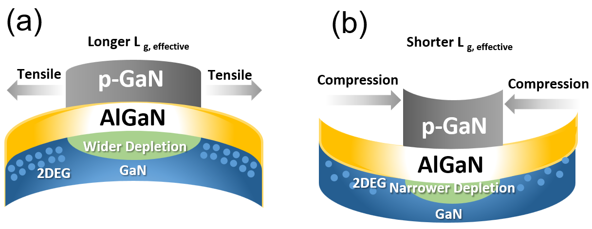
This disparity can be explained by the piezoelectric effect on GaN High-Electron-Mobility Transistors (HEMTs), as illustrated in
Figure 12a,b. In the context of AlGaN, compressive stress is expected to occur due to lattice and thermal mismatch after epitaxy growth using MOCVD [
11]. However, the mechanical stress induced by the molding compound can transform the compressive stress into tensile stress in AlGaN [
12]. This transformation leads to a longer effective channel length and a wider depletion region in devices with AlGaN under tensile strain, resulting in a lower I
G at reverse stress [
13,
14,
15], as
Figure 12a shows.
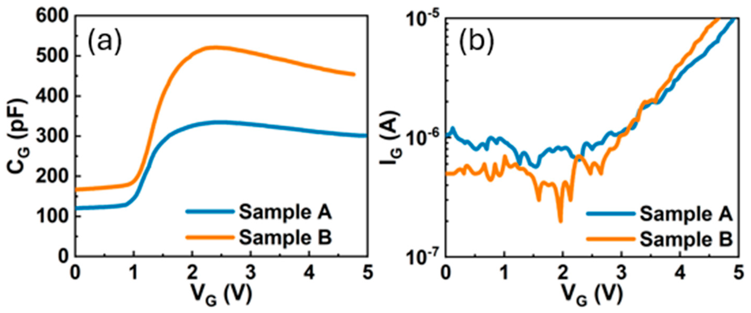
As shown in
Figure 13a,b, Sample B exhibits a larger gate capacitance (C
G) at low gate voltage (V
G < 1 V) and a lower gate leakage current (I
G) for V
G < 2 V when compared to Sample A. These observations suggest that Sample B possesses a wider depletion region beneath the p-GaN gate, resulting in a reduced gate leakage current in the off-state (I
GOFF) below 2V. This characteristic is hypothesized to correlate with variations in the width of the depletion region under the p-GaN gate, which is induced by mechanical stress originating from the packaging process.
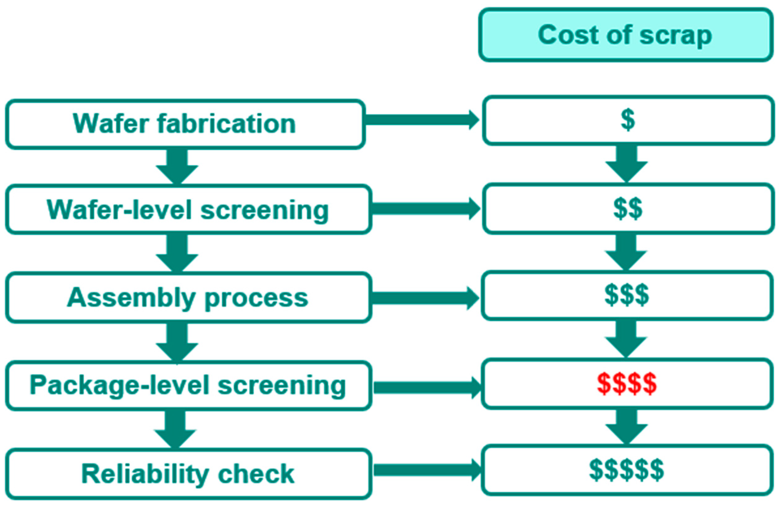
Allowing the die with a gate metal defect to proceed in the manufacturing supply chain increases the cost of scrap at a later stage, as
Figure 1 shows; therefore, a wafer-level screening methodology is needed. At the wafer-evel (Sample A), the depletion region under the p-GaN gate is narrower, as
Figure 12b shows, making it more challenging to detect changes in gate controllability, such as the discrepancy shown in
Figure 12. Since there is a subtle change in the leakage current at V
G = −60 V at the package-level, as
Figure 12a shows, with high electrical field at the gate edge, the leakage current may also have a subtle change that can be detected by repeating the measurement of I
DSS with high electrical field at the gate edge. After going through several types of testing sequencing, repeating I
DSS at V
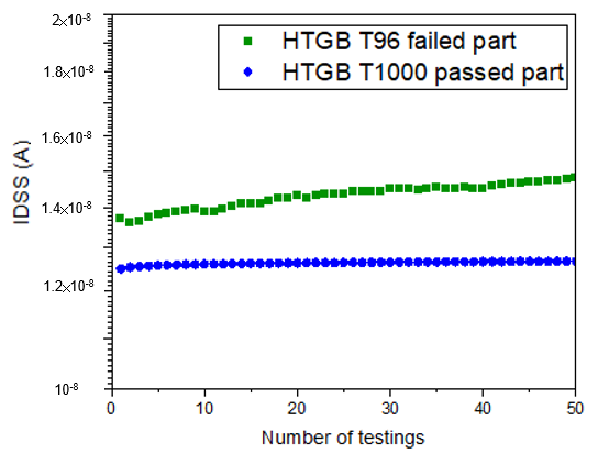
D = 650 V is the most promising screening test plan with 50 times at the wafer-level. The number of tests is plotted on the x-axis and that of I
DSS readings on the y-axis and we see that I
DSS leakage goes up with the number of testing times for gate metal defect parts, as
Figure 14 shows. For parts passing HTGB 1000 h stress, repeating the I
DSS test merely shows no change at a fresh wafer test. Therefore, the applied compression stress after wafer processing at the gate reduces the internal electric field in AlGaN, thereby suppressing the leakage current (I
GOFF) caused by Fowler–Nordheim (FN) tunneling when the strained device was under reverse bias [
13]. However, the presence of a gate metal defect affects the controllability of the gate, leading to minimal changes in control of the peak electrical field by the gate toward the drain side. Detectability at the package-level has introduced tensile stress from packaging and electrical crowding by the gate into gate reverse bias. Therefore, the introduction of a peak electric field by the gate toward the drain site may boost the sensitivity of gate-related defect detection at the wafer-level with compressive stress.
The comprehensive fabrication qualification involved the assembly of three staggered production lots, each yielding approximately 1500 units. A thorough screening protocol was subsequently implemented at the package-level on the final devices. This package-level screening utilized a high gate-voltage stress condition, V
G = −60 V, specifically targeting latent defects. This initial inspection successfully identified 21 parts exhibiting the specific electrical failure signature illustrated in
Figure 11b. All 21 flagged units were then subjected to the standard High-Temperature Gate Bias (HTGB) reliability test, following the established conditions depicted in
Figure 6. Crucially, every single one of these screened units failed prematurely, registering failures in both I
DSS before the T1000 milestone, which is consistent with the failure mechanism previously observed in the smaller, preliminary HTGB sample sets. To confirm the statistical validity of the sampling plan, a comparative failure ratio analysis was performed: the sampling HTGB failure rate was 1 out of 231 (0.43%), while the package-level screening identified 21 failures out of 4269 parts (0.49%). The close correlation between these two ratios validates the fact that the samples drawn from the three qualification lots were statistically representative of the entire population’s defectivity level.
To move beyond simple pass/fail screening and to sensitively detect subtle electrical degradation prior to packaging, a refined characterization technique was developed and deployed. This method leverages the cumulative effect of repeating I
DSS pulse tests to magnify the influence of minor electric field perturbations within the device structure. By plotting the I
DSS reading as a function of the number of test cycles, a clear pattern of I
DSS instability or drift could be established, as visually demonstrated in
Figure 14. This enhanced characterization test plan, featuring multiple I
DSS pulse cycles, was subsequently implemented as a pre-packaging, wafer-level HTGB verification screen on the new production lots. After effectively filtering out and excluding the dies that exhibited I
DSS drifting behavior during these wafer-level pulse tests, a total of 231 non-drifting dies were randomly selected, assembled into packages, and committed to the final HTGB qualification test. The rigorous application of this new, preemptive screening methodology yielded a definitive result: there were zero failures recorded after completing the full 1000 h of HTGB stress, a significant achievement that underscores the efficacy of the improved screening protocol, as summarized in the final yield chart of
Figure 15.
