
Fabrication of Large-Area Silicon Spherical Microlens Arrays by Thermal Reflow and ICP Etching

 , ,
, ,
Abstract
1. Introduction
2. Materials and Methods
2.1. Materials
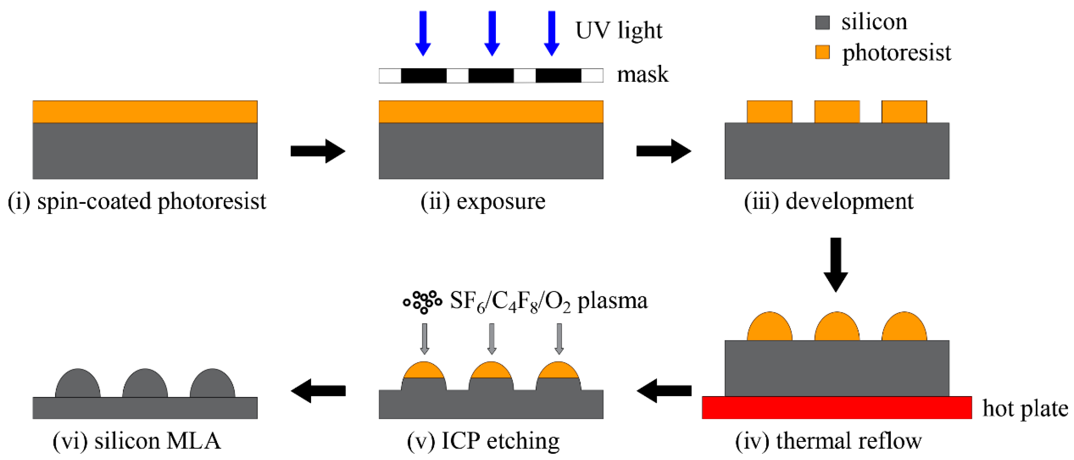
2.2. Experiment
2.3. Characterization
3. Results and Discussion
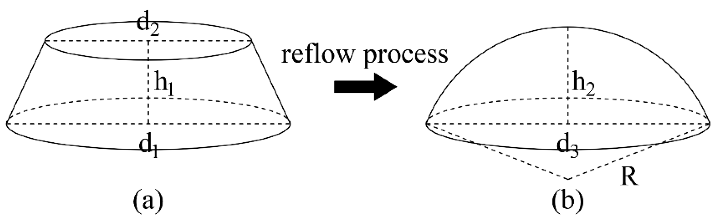
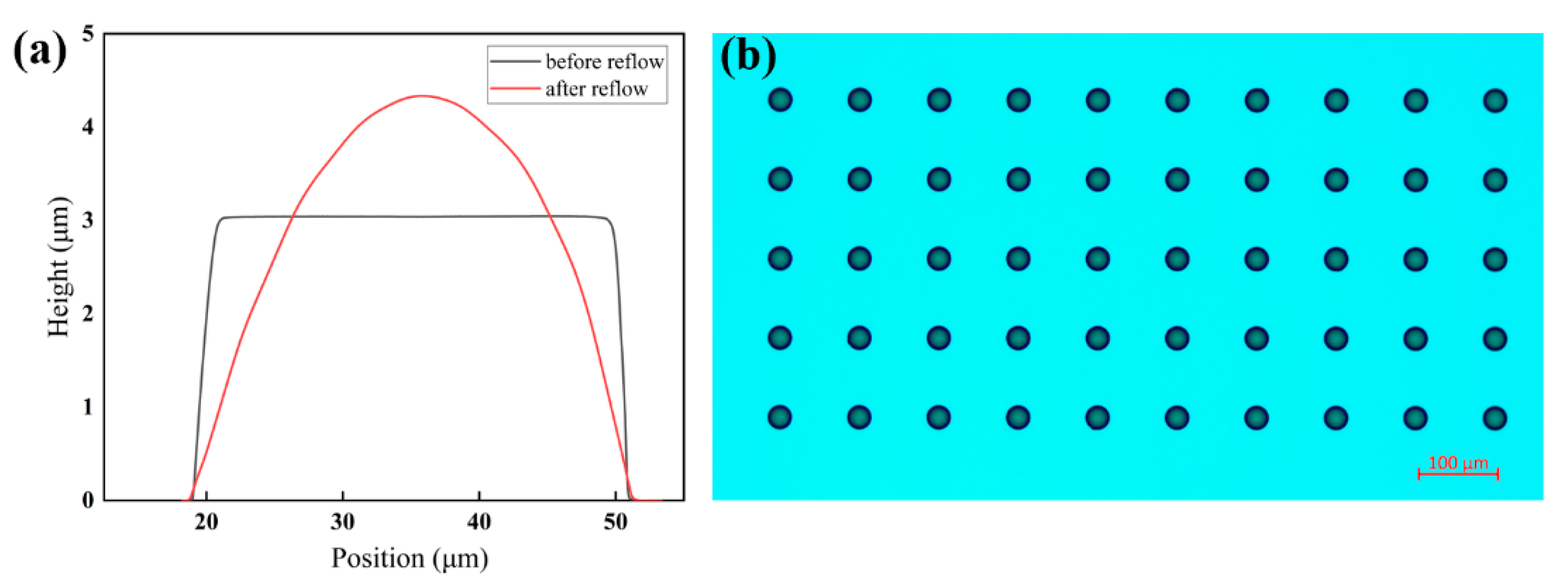
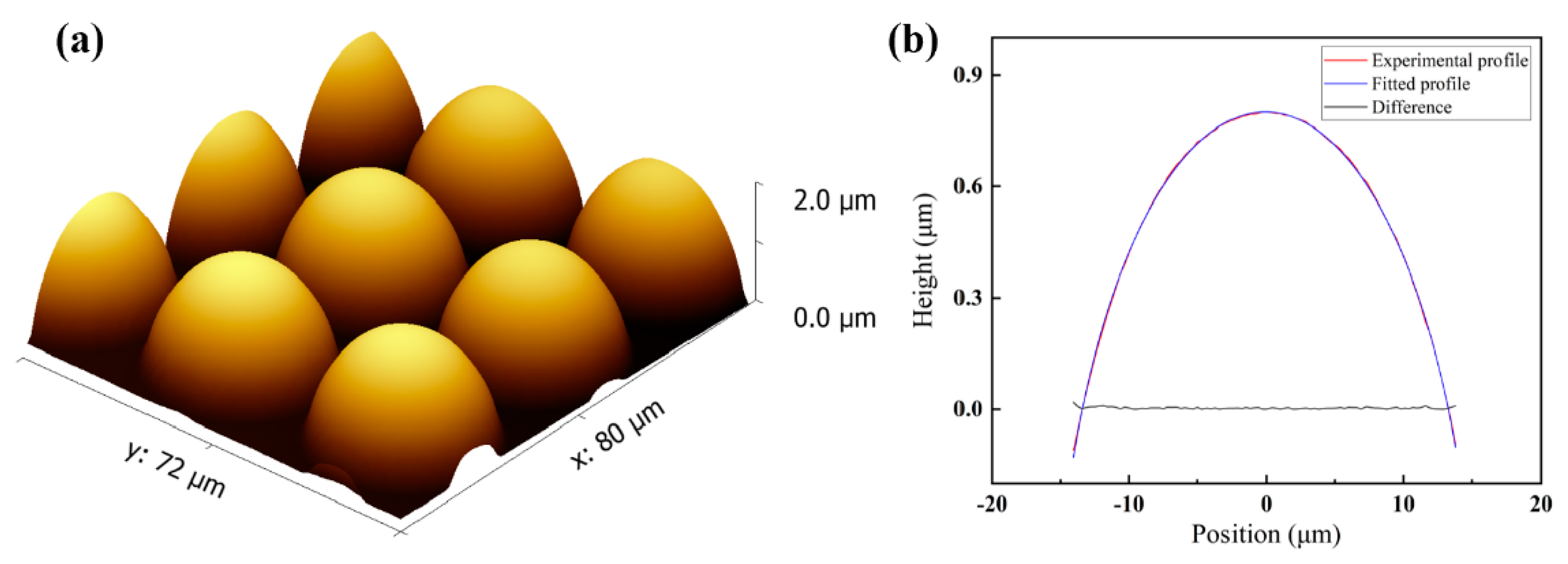
3.1. Results and Analysis of Thermal Reflow
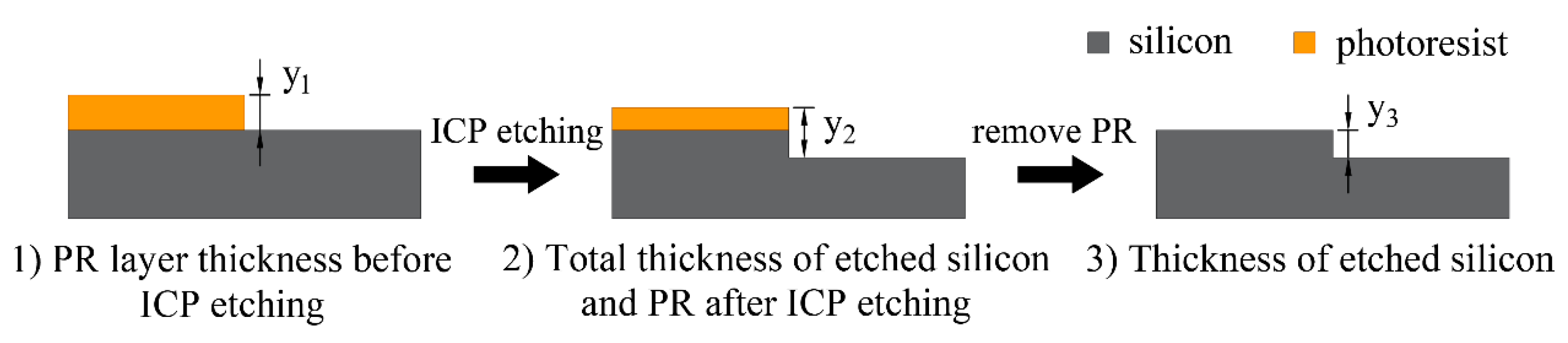
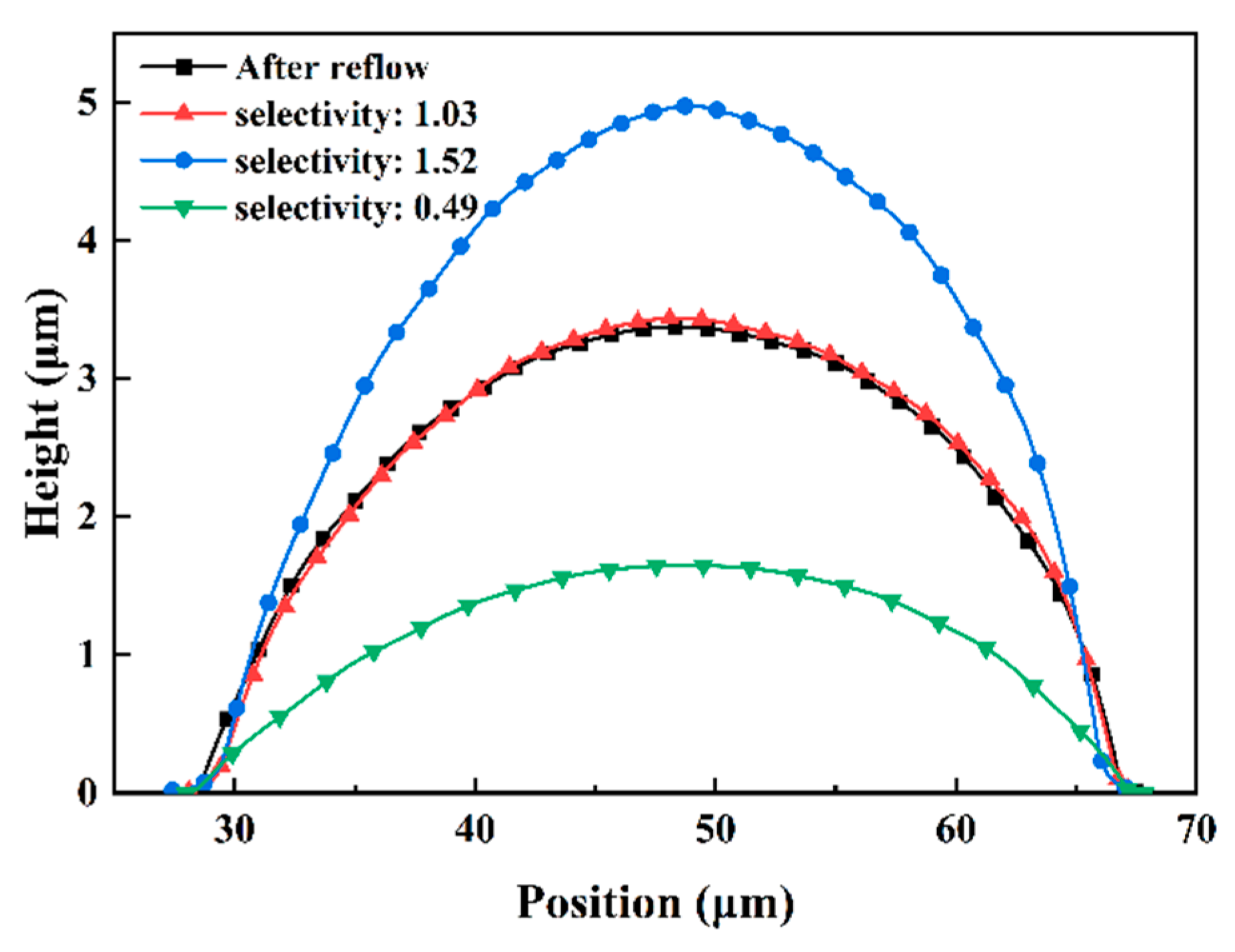
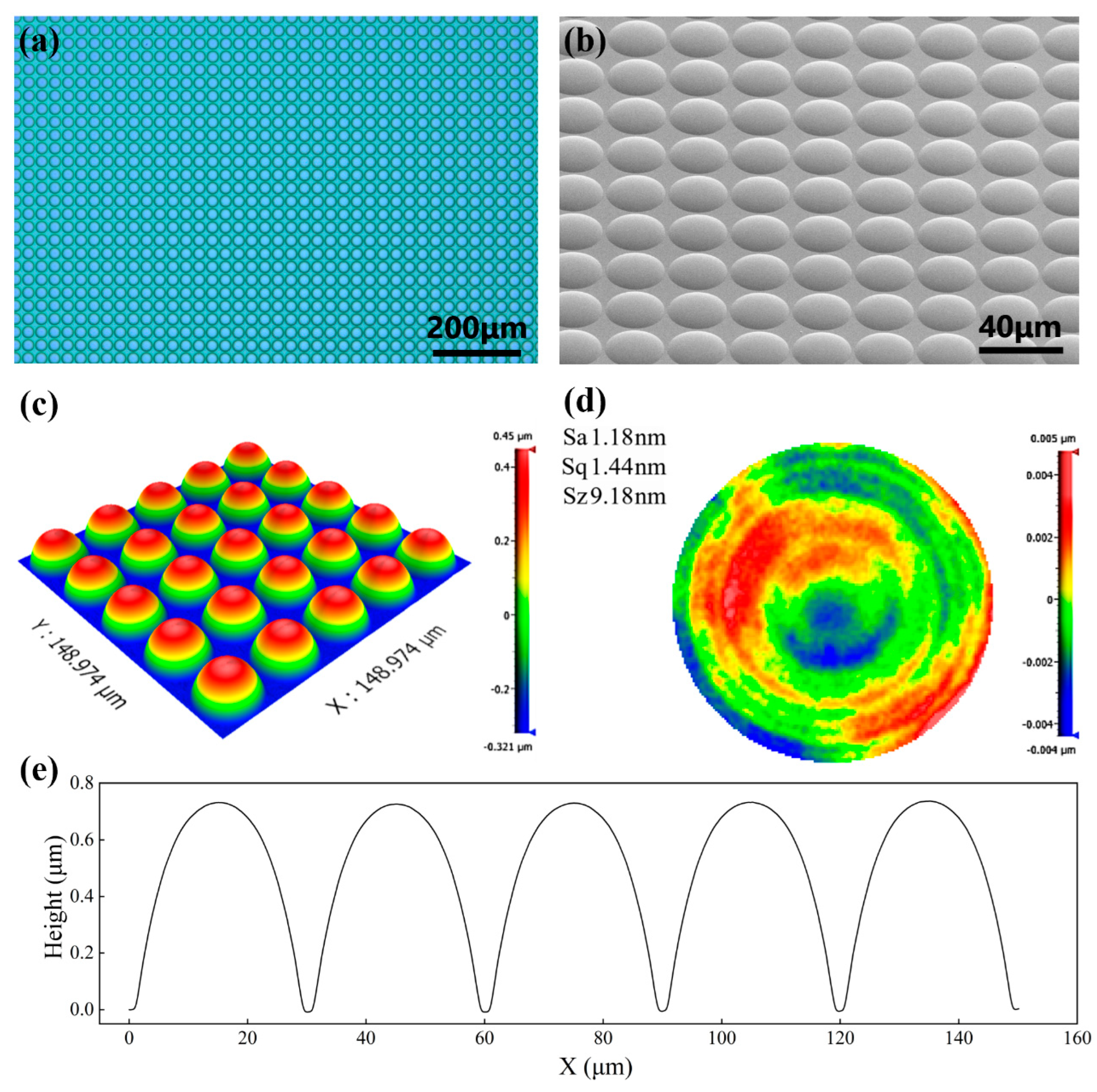
3.2. Results and Analysis of ICP Etching

| Number | RF Power (W) | Gas Flow (sccm) | Height (μm) | Etching Rate (μm/min) | SR | |||||
|---|---|---|---|---|---|---|---|---|---|---|
| SF6 | C4F8 | O2 | y1 | y1 | y3 | EPR | ESi | |||
| 1 | 35 | 10 | 30 | 0 | 3.343 | 3.258 | 0.507 | 0.197 | 0.169 | 0.86 |
| 2 | 35 | 10 | 30 | 40 | 2.762 | 3.101 | 1.116 | 0.259 | 0.372 | 1.44 |
| 3 | 15 | 10 | 30 | 40 | 2.861 | 3.158 | 0.660 | 0.121 | 0.220 | 1.82 |
| 4 | 20 | 10 | 30 | 40 | 2.971 | 3.266 | 0.749 | 0.152 | 0.250 | 1.65 |
| 5 | 25 | 10 | 30 | 40 | 2.881 | 3.195 | 0.863 | 0.183 | 0.288 | 1.57 |
| 6 | 30 | 10 | 30 | 40 | 2.822 | 3.132 | 0.934 | 0.208 | 0.311 | 1.50 |
| 7 | 35 | 6 | 30 | 40 | 3.308 | 3.305 | 0.774 | 0.259 | 0.258 | 1.00 |
| 8 | 35 | 7 | 30 | 40 | 3.106 | 3.183 | 0.850 | 0.257 | 0.283 | 1.10 |
| 9 | 35 | 8 | 30 | 40 | 3.467 | 3.623 | 0.916 | 0.253 | 0.305 | 1.21 |
| 10 | 35 | 9 | 30 | 40 | 3.513 | 3.759 | 1.012 | 0.255 | 0.337 | 1.32 |
| 11 | 35 | 10 | 20 | 40 | 3.525 | 4.797 | 2.276 | 0.335 | 0.759 | 2.27 |
| 12 | 35 | 10 | 25 | 40 | 3.559 | 4.303 | 1.593 | 0.283 | 0.531 | 1.88 |
| 13 | 35 | 10 | 35 | 40 | 3.302 | 3.554 | 0.935 | 0.228 | 0.312 | 1.37 |
| 14 | 35 | 10 | 40 | 40 | 3.140 | 3.326 | 0.859 | 0.224 | 0.286 | 1.28 |
| 15 | 35 | 10 | 30 | 30 | 2.966 | 3.182 | 0.922 | 0.235 | 0.307 | 1.31 |
| 16 | 35 | 10 | 30 | 35 | 2.926 | 3.192 | 1.004 | 0.246 | 0.335 | 1.36 |
| 17 | 35 | 10 | 30 | 45 | 2.950 | 3.325 | 1.188 | 0.271 | 0.396 | 1.46 |
| 18 | 35 | 10 | 30 | 50 | 2.901 | 3.364 | 1.331 | 0.290 | 0.444 | 1.53 |

4. Conclusions
Author Contributions
Funding
Data Availability Statement
Conflicts of Interest
References
- Chen, M.; Zhang, Z.; Wu, H.; Xie, S.; Wang, H. Otsu-Kmeans gravity-based multi-spots center extraction method for microlens array imaging system. Opt. Lasers Eng. 2022, 152, 106968. [Google Scholar] [CrossRef]
- Zhong, Y.; Yu, H.; Wen, Y.; Zhou, P.; Guo, H.; Zou, W.; Lv, X.; Liu, L. Novel optofluidic imaging system integrated with tunable microlens arrays. ACS Appl. Mater. Interfaces 2023, 15, 11994–12004. [Google Scholar] [CrossRef] [PubMed]
- Yu, C.; Yang, J.; Song, N.; Sun, C.; Wang, M.; Feng, S. Microlens array snapshot hyperspectral microscopy system for the biomedical domain. Appl. Optics 2021, 60, 1896–1902. [Google Scholar] [CrossRef] [PubMed]
- Park, M.K.; Park, H.; Joo, K.I.; Lee, T.H.; Kwon, K.C.; Erdenebat, M.U.; Lim, Y.T.; Kim, N.; Kim, H.R. Fast-switching laterally virtual-moving microlens array for enhancing spatial resolution in light-field imaging system without degradation of angular sampling resolution. Sci. Rep. 2019, 9, 11297. [Google Scholar] [CrossRef] [PubMed]
- Zhou, X.; Peng, Y.; Peng, R.; Zeng, X.; Zhang, Y.A.; Guo, T. Fabrication of large-scale microlens arrays based on screen printing for integral imaging 3D display. ACS Appl. Mater. Interfaces 2016, 8, 24248–24255. [Google Scholar] [CrossRef] [PubMed]
- Im, B.; Prasetyo, F.D.; Yudistira, H.T.; Khalil, S.M.; Cho, D.H.; Byun, D. Drop-on-demand electrohydrodynamic jet printing of microlens array on flexible substrates. ACS Appl. Polym. Mater. 2023, 5, 2264–2271. [Google Scholar] [CrossRef]
- Liu, X.Q.; Yu, L.; Yang, S.N.; Chen, Q.D.; Wang, L.; Juodkazis, S.; Sun, H.B. Optical nanofabrication of concave microlens arrays. Laser Photonics Rev. 2019, 13, 1800272. [Google Scholar] [CrossRef]
- Li, D.; Wang, W.; Gao, S.; Gao, Y.; Cai, Y.; Hao, Z.; Wen, Z. Controlling self-healing of optical field based on moiré dual-microlens arrays. New J. Phys. 2023, 25, 083023. [Google Scholar] [CrossRef]
- Chen, X.; Zhang, G.; Wang, M.Y.; Yu, H. A thin format vision-based tactile sensor with a microlens array (MLA). IEEE Sens. J. 2022, 22, 22069–22076. [Google Scholar] [CrossRef]
- Agarwal, A.K.; Pant, K.K.; Mishra, S.K. Development of microlens arrays with large focal number and high fill factor for wavefront sensing applications. IEEE Sens. J. 2021, 21, 20990–20997. [Google Scholar] [CrossRef]
- Zhao, Z.; Yin, T.; To, S.; Zhu, Z.; Zhuang, Z. Material removal energy in ultraprecision machining of micro-lens arrays on single crystal silicon by slow tool servo. J. Clean Prod. 2022, 335, 130295. [Google Scholar] [CrossRef]
- Huang, Y.; Li, S.; Zhang, J.; Yang, C.; Kong, Y.; Liu, W. Research on surface quality difference of microlens array fabricated by fast tool servo cutting. IEEE Photonics J. 2021, 13, 1–9. [Google Scholar] [CrossRef]
- Wang, S.; Kong, L.; Wang, C.; Cheung, C. Ultra-precision manufacturing of microlens arrays using an optimum machining process chain. Opt. Express. 2023, 31, 2234–2247. [Google Scholar] [CrossRef] [PubMed]
- Wang, Z.; Chen, Z.; Zhang, X. Profile compensation for single-point diamond turning of microlens array. Nanomanuf. Metrol. 2022, 5, 403–411. [Google Scholar] [CrossRef]
- Yuan, W.; Li, L.H.; Lee, W.B.; Chan, C.Y. Fabrication of microlens array and its application: A review. Chin. J. Mech. Eng. 2018, 31, 1–9. [Google Scholar] [CrossRef]
- Li, R.; Li, C.; Yan, M.; Li, M.; Lin, C.; Dai, S.; Song, B.; Xu, T.; Zhang, P. Fabrication of chalcogenide microlens arrays by femtosecond laser writing and precision molding. Ceram. Int. 2023, 49, 15865–15873. [Google Scholar] [CrossRef]
- Gissibl, T.; Thiele, S.; Herkommer, A.; Giessen, H. Two-photon direct laser writing of ultracompact multi-lens objectives. Nat. Photonics 2016, 10, 554–560. [Google Scholar] [CrossRef]
- Deng, H.; Qi, D.; Wang, X.; Liu, Y.; Shangguan, S.; Zhang, J.; Shen, X.; Liu, X.; Wang, J.; Zheng, H. Femtosecond laser writing of infrared microlens arrays on chalcogenide glass. Opt. Laser Technol. 2023, 159, 108953. [Google Scholar] [CrossRef]
- Cunha, J.; Garcia, I.S.; Santos, J.D.; Fernandes, J.; González-Losada, P.; Silva, C.; Gaspar, J.; Cortez, A.; Sampaio, M.; Aguiam, D.E. Assessing tolerances in direct write laser grayscale lithography and reactive ion etching pattern transfer for fabrication of 2.5 D Si master molds. Micro. Nano. Eng. 2023, 19, 100182. [Google Scholar] [CrossRef]
- Bekker, C.; Arshad, M.J.; Cilibrizzi, P.; Nikolatos, C.; Lomax, P.; Wood, G.S.; Cheung, R.; Knolle, W.; Ross, N.; Gerardot, B.; et al. Scalable fabrication of hemispherical solid immersion lenses in silicon carbide through grayscale hard-mask lithography. Appl. Phys. Lett. 2023, 122, 173507. [Google Scholar] [CrossRef]
- Chou, S.Y.; Krauss, P.R.; Renstrom, P.J. Imprint of sub-25 nm vias and trenches in polymers. Appl. Phys. Lett. 1995, 67, 3114–3116. [Google Scholar] [CrossRef]
- Deshmukh, S.S.; Goswami, A. Microlens array through induction-aided hot embossing: Fabrication, optimization, and characterization. Mater. Manuf. Process. 2022, 37, 1540–1554. [Google Scholar] [CrossRef]
- Graczyk, M.; Cattoni, A.; Rösner, B.; Seniutinas, G.; Löfstrand, A.; Kvennefors, A.; Mailly, D.; David, C.; Maximov, I. Nanoimprint stamps with ultra-high resolution: Optimal fabrication techniques. Microelectron. Eng. 2018, 190, 73–78. [Google Scholar] [CrossRef]
- Li, Y.; Li, K.; Gong, F. Fabrication and optical characterization of polymeric aspherical microlens array using hot embossing technology. Appl. Sci. 2021, 11, 882. [Google Scholar] [CrossRef]
- Qiu, J.; Li, M.; Zhu, J.; Ji, C. Fabrication of microlens array with well-defined shape by spatially constrained thermal reflow. J. Micromech. Microeng. 2018, 28, 085015. [Google Scholar] [CrossRef]
- Liang, X.; Yan, M.; Xu, Y.; Zhang, T.; Zhang, D.; Zhang, C.; Wang, B.; Yi, F.; Liu, J. The fabrication of microlens array in PMMA material with the assistant of nickel pillars by LIGA technology and thermal reflow method. Microsyst. Technol. 2023, 29, 763–771. [Google Scholar] [CrossRef]
- Gong, S.; Qiu, J.; Li, M. A facile method for fabricating microlens array with diverse morphologies at general thermal reflow conditions. Jpn. J. Appl. Phys. 2022, 61, 100902. [Google Scholar] [CrossRef]
- Sun, R.; Zhang, X.; Zhang, Y.; Zhang, X.; Hu, F. Fabrication of microlens arrays with high filling factors by combining a thermal reflow and parylene CVD technique and the applications on OLEDs. Appl. Optics 2022, 61, 3048–3053. [Google Scholar] [CrossRef] [PubMed]
- Mukaida, M.; Yan, J. Fabrication of hexagonal microlens arrays on single-crystal silicon using the tool-servo driven segment turning method. Micromachines 2017, 8, 323. [Google Scholar] [CrossRef]
- Hua, J.G.; Ren, H.; Jia, A.; Tian, Z.N.; Wang, L.; Juodkazis, S.; Chen, Q.D.; Sun, H.B. Convex silica microlens arrays via femtosecond laser writing. Opt. Lett. 2020, 45, 636–639. [Google Scholar] [CrossRef]
- Deng, Z.; Yang, Q.; Chen, F.; Meng, X.; Bian, H.; Yong, J.; Shan, C.; Hou, X. Fabrication of large-area concave microlens array on silicon by femtosecond laser micromachining. Opt. Lett. 2015, 40, 1928–1931. [Google Scholar] [CrossRef] [PubMed]
- Asif, M.H.; Graczyk, M.; Heidari, B.; Maximov, I. Comparison of UV-curable materials for high-resolution polymer nanoimprint stamps. Micro. Nano. Eng. 2022, 14, 100118. [Google Scholar] [CrossRef]
- Sun, Q.; Tang, J.; Shen, L.; Lan, J.; Shen, Z.; Xiao, J.; Chen, X.; Zhang, J.; Wu, Y.; Xu, J.; et al. Fabrication of high precision silicon spherical microlens arrays by hot embossing process. Micromachines 2022, 13, 899. [Google Scholar] [CrossRef] [PubMed]
- Gu, Z.; Wu, M.; Gao, Y.; Chen, Y.; Gu, C.; Ren, H.; Wang, C.; Chen, H.; Dai, S.; Shen, X. Rapid fabrication of highly integrated and high numerical aperture chalcogenide glass microlens arrays. Infrared Phys. Technol. 2023, 129, 104537. [Google Scholar] [CrossRef]
- Gong, S.; Shi, C.; Li, M. Flow performance and its effect on shape formation in pdms assisted thermal reflow process. Appl. Sci. 2022, 12, 8282. [Google Scholar] [CrossRef]
- Xiao, J.; Luo, Y.; Niu, M.; Wang, Q.; Wu, J.; Liu, X.; Xu, J. Study of imbibition in various geometries using phase field method. Capillarity 2019, 2, 57–65. [Google Scholar] [CrossRef]
- Goharzadeh, A.; Fatt, Y.Y.; Sangwai, J.S. Effect of TiO2-SiO2 hybrid nanofluids on enhanced oil recovery process under different wettability conditions. Capillarity 2023, 8, 1–10. [Google Scholar] [CrossRef]
- Qiu, J.; Li, M.; Ye, H.; Zhu, J.; Ji, C. Fabrication of high fill-factor microlens array using spatially constrained thermal reflow. Sens. Actuator A-Phys. 2018, 279, 17–26. [Google Scholar] [CrossRef]
- Erjawetz, J.; Collé, D.; Ekindorf, G.; Heyl, P.; Ritter, D.; Reddy, A.; Schift, H. Bend the curve–shape optimization in laser grayscale direct write lithography using a single figure of merit. Micro. Nano. Eng. 2022, 15, 100137. [Google Scholar] [CrossRef]
- Shi, Z.; Jefimovs, K.; Stampanoni, M.; Romano, L. High aspect ratio arrays of Si nano-pillars using displacement Talbot lithography and gas-MacEtch. Mater. Sci. Semicond. Process 2023, 157, 107311. [Google Scholar] [CrossRef]
- Luo, Z.; Shao, S.; Wu, T. Characterization of AlN and AlScN film ICP etching for micro/nano fabrication. Microelectron. Eng. 2021, 242, 111530. [Google Scholar] [CrossRef]
- Huang, Y.; Tang, F.; Guo, Z.; Wang, X. Accelerated ICP etching of 6H-SiC by femtosecond laser modification. Appl. Surf. Sci. 2019, 488, 853–864. [Google Scholar] [CrossRef]
- Chang, B.; Leussink, P.; Jensen, F.; Hübner, J.; Jansen, H. DREM: Infinite etch selectivity and optimized scallop size distribution with conventional photoresists in an adapted multiplexed Bosch DRIE process. Microelectron. Eng. 2018, 191, 77–83. [Google Scholar] [CrossRef]
- Hu, R.; Ma, H.; Yin, H.; Xu, J.; Chen, K.; Yu, L. Facile 3D integration of Si nanowires on Bosch-etched sidewalls for stacked channel transistors. Nanoscale 2020, 12, 2787–2792. [Google Scholar] [CrossRef] [PubMed]
- Zhang, Y.; Wu, Y.; Sun, Q.; Shen, L.; Lan, J.; Guo, L.; Shen, Z.; Wang, X.; Xiao, J.; Xu, J. Inductively coupled plasma dry etching of silicon deep trenches with extremely vertical smooth sidewalls used in micro-optical gyroscopes. Micromachines 2023, 14, 846. [Google Scholar] [CrossRef] [PubMed]
- Wang, X.; Dong, X.; Xiao, J.; Zhang, Y.; Xu, J.; Liu, S.; Gao, L. Quantum effects of gas flow in nanochannels. Nanotechnol. Rev. 2021, 10, 254–263. [Google Scholar] [CrossRef]
- Aydinoglu, F.; Pan, A.; Zhu, C.; Cui, B. Effect of oxygen plasma cleaning on nonswitching pseudo-Bosch etching of high aspect ratio silicon pillars. J. Vac. Sci. Technol. B 2020, 38, 012804. [Google Scholar] [CrossRef]
| Number | Cylinder before Reflow (μm) | Microlens after Reflow (μm) | k | ||||
|---|---|---|---|---|---|---|---|
| d1 | d2 | h1 | d3 | h2 | R | ||
| 1 | 32.65 | 28.08 | 3.03 | 32.88 | 4.31 | 33.51 | 0.850 |
| 2 | 37.50 | 33.48 | 3.00 | 38.28 | 4.27 | 45.03 | 0.841 |
| 3 | 42.73 | 38.18 | 3.00 | 42.53 | 4.27 | 55.06 | 0.797 |
| 4 | 47.73 | 43.08 | 2.98 | 47.50 | 4.09 | 70.92 | 0.758 |
| 5 | 32.60 | 28.55 | 2.65 | 32.33 | 3.75 | 36.88 | 0.804 |
| 6 | 36.20 | 33.85 | 2.63 | 36.45 | 3.71 | 46.60 | 0.774 |
| 7 | 42.13 | 38.45 | 2.62 | 42.40 | 3.53 | 65.39 | 0.753 |
| 8 | 46.95 | 43.53 | 2.61 | 47.35 | 3.36 | 85.11 | 0.709 |
Disclaimer/Publisher’s Note: The statements, opinions and data contained in all publications are solely those of the individual author(s) and contributor(s) and not of MDPI and/or the editor(s). MDPI and/or the editor(s) disclaim responsibility for any injury to people or property resulting from any ideas, methods, instructions or products referred to in the content. |
© 2024 by the authors. Licensee MDPI, Basel, Switzerland. This article is an open access article distributed under the terms and conditions of the Creative Commons Attribution (CC BY) license (https://creativecommons.org/licenses/by/4.0/).
Share and Cite
Wu, Y.; Dong, X.; Wang, X.; Xiao, J.; Sun, Q.; Shen, L.; Lan, J.; Shen, Z.; Xu, J.; Du, Y. Fabrication of Large-Area Silicon Spherical Microlens Arrays by Thermal Reflow and ICP Etching. Micromachines 2024, 15, 460. https://doi.org/10.3390/mi15040460
Wu Y, Dong X, Wang X, Xiao J, Sun Q, Shen L, Lan J, Shen Z, Xu J, Du Y. Fabrication of Large-Area Silicon Spherical Microlens Arrays by Thermal Reflow and ICP Etching. Micromachines. 2024; 15(4):460. https://doi.org/10.3390/mi15040460
Chicago/Turabian StyleWu, Yu, Xianshan Dong, Xuefang Wang, Junfeng Xiao, Quanquan Sun, Lifeng Shen, Jie Lan, Zhenfeng Shen, Jianfeng Xu, and Yuqingyun Du. 2024. "Fabrication of Large-Area Silicon Spherical Microlens Arrays by Thermal Reflow and ICP Etching" Micromachines 15, no. 4: 460. https://doi.org/10.3390/mi15040460
APA StyleWu, Y., Dong, X., Wang, X., Xiao, J., Sun, Q., Shen, L., Lan, J., Shen, Z., Xu, J., & Du, Y. (2024). Fabrication of Large-Area Silicon Spherical Microlens Arrays by Thermal Reflow and ICP Etching. Micromachines, 15(4), 460. https://doi.org/10.3390/mi15040460