
Novel SiC Trench MOSFET with Improved Third-Quadrant Performance and Switching Speed

Abstract
1. Introduction
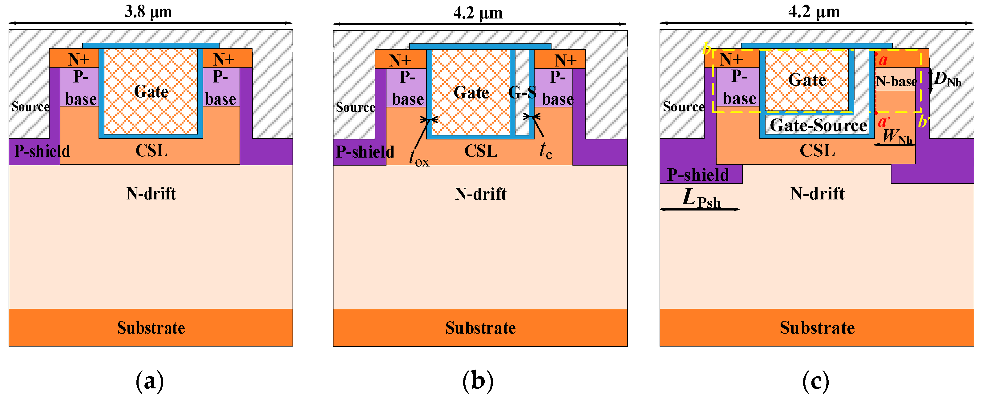
2. Device Structure and Mechanism
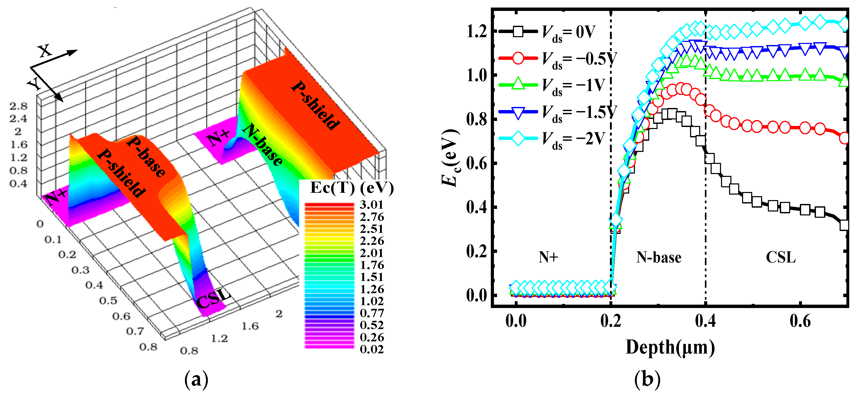
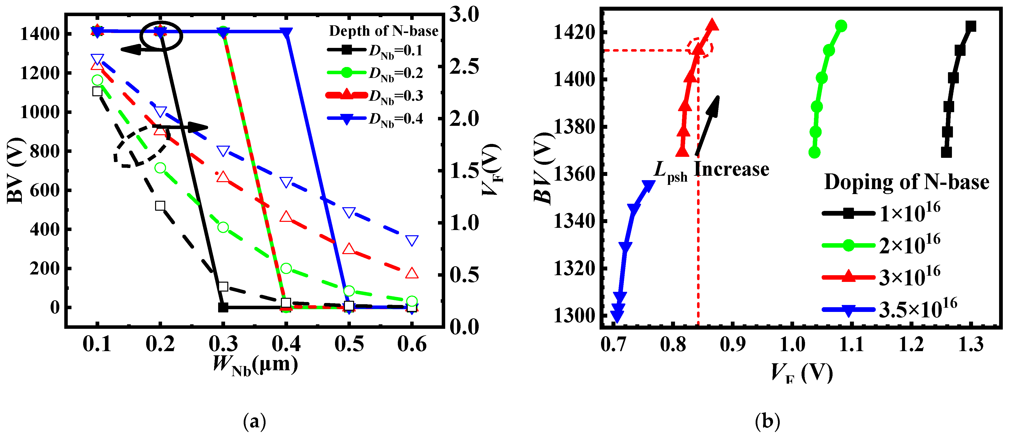
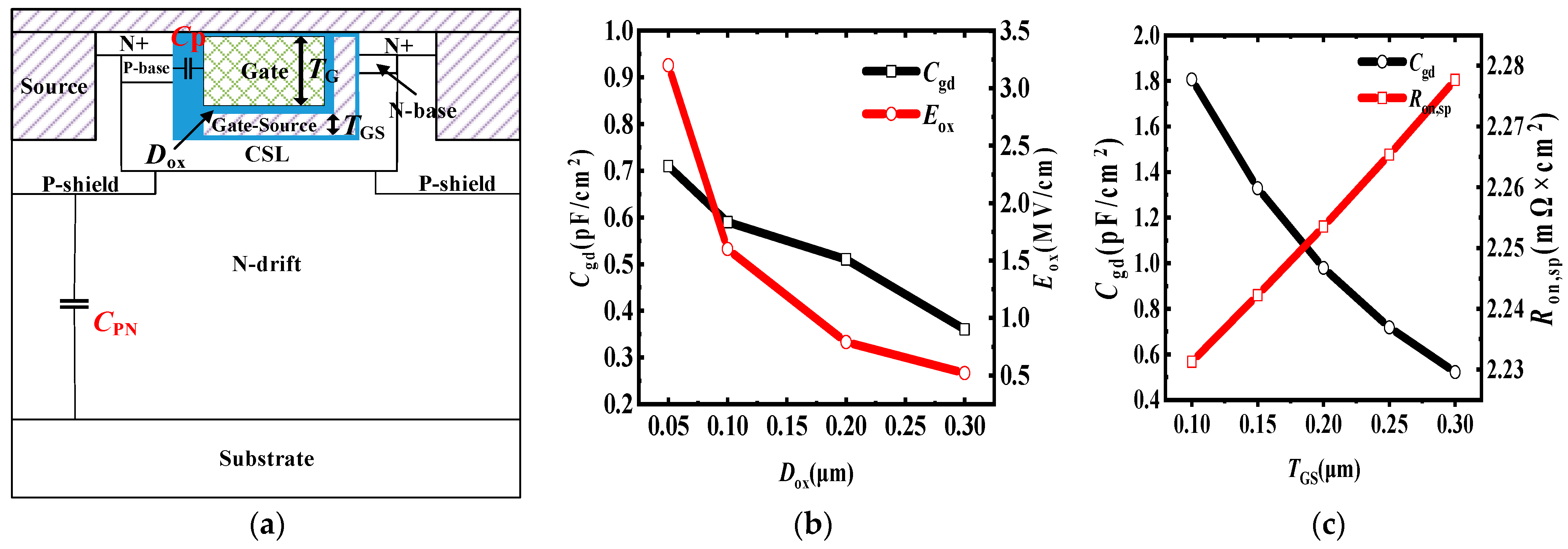
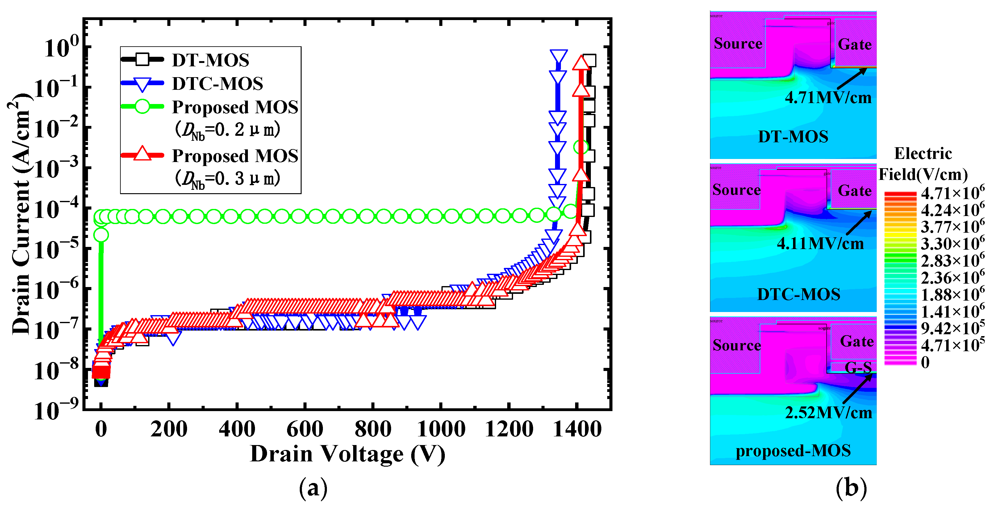
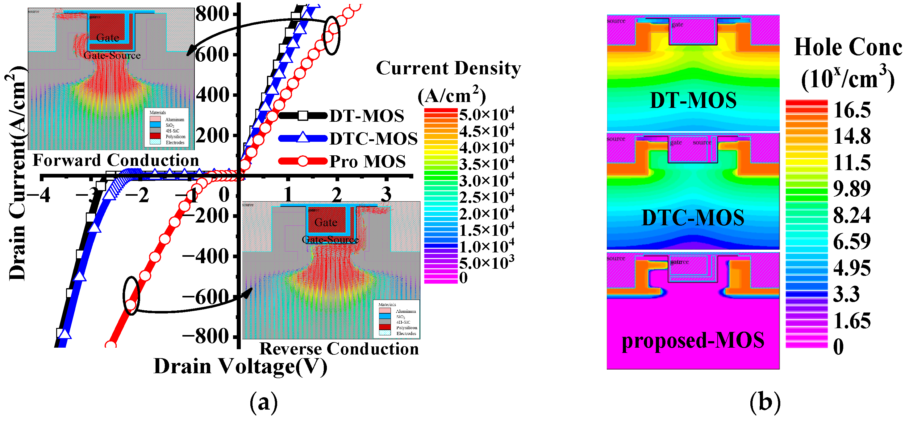
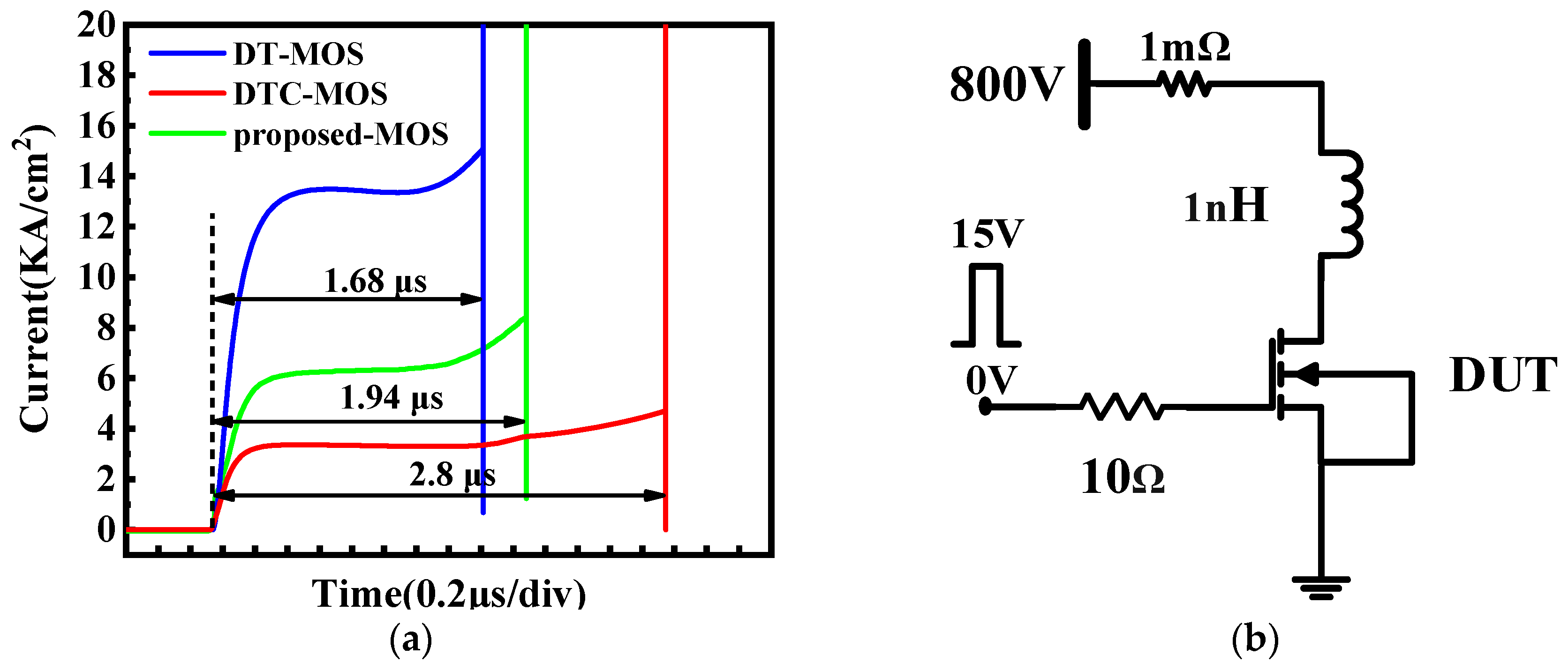
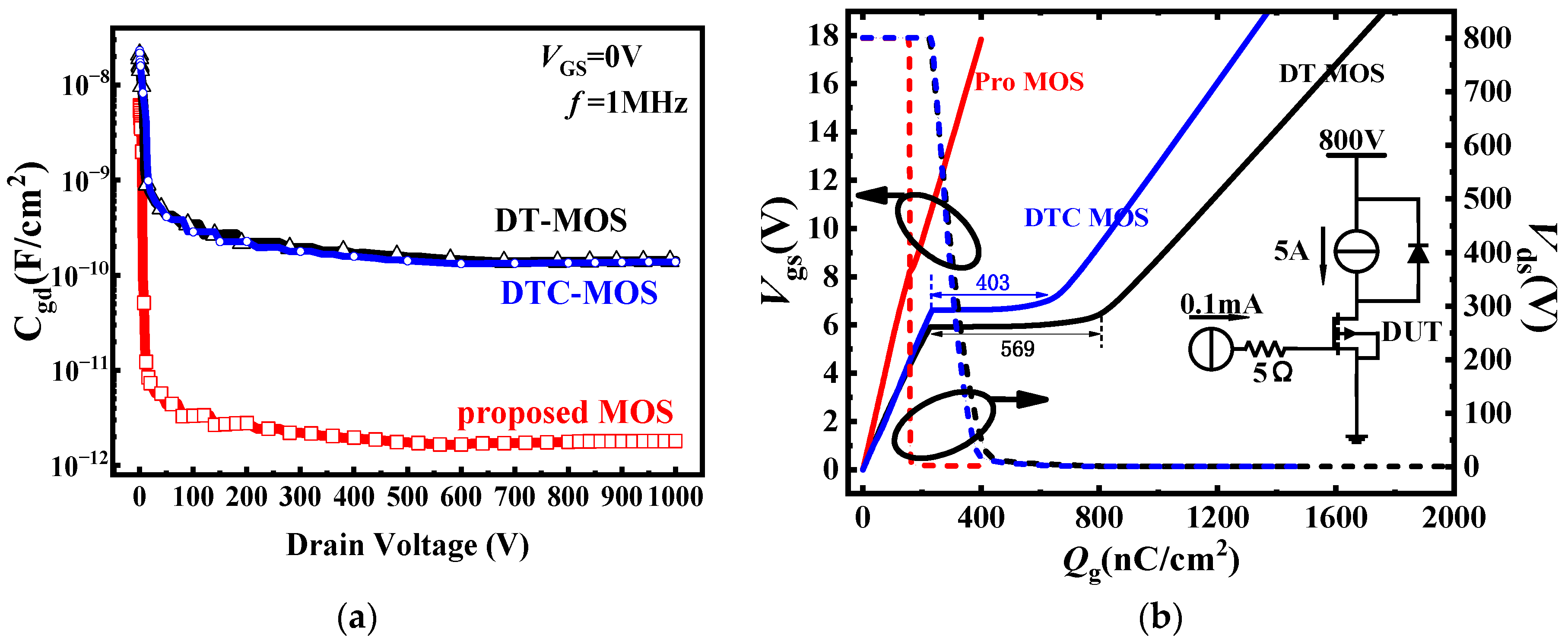
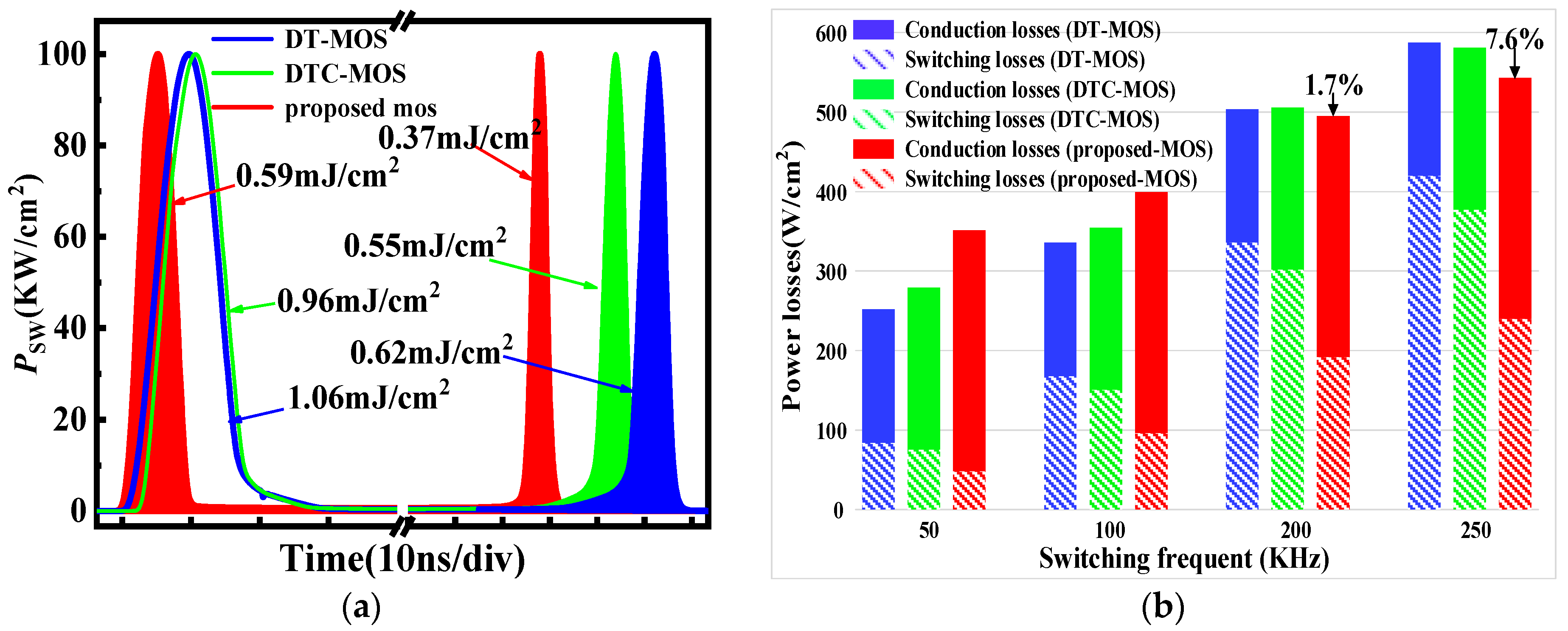
3. Simulation Results and Analysis
4. Conclusions
Author Contributions
Funding
Data Availability Statement
Conflicts of Interest
References
- Millan, J.; Godignon, P.; Perpina, X.; Perez-Tomas, A.; Rebollo, J. A Survey of Wide Bandgap Power Semiconductor Devices. IEEE Trans. Power Electron. 2014, 29, 2155–2163. [Google Scholar] [CrossRef]
- Hudgins, J.L.; Simin, G.S.; Santi, E.; Khan, M.A. An assessment of wide bandgap semiconductors for power devices. IEEE Trans. Power Electron. 2003, 18, 907–914. [Google Scholar] [CrossRef]
- Hazra, S.; De, A.K.; Cheng, L.; Palmour, J.; Schupbach, M.; Hull, B.A.; Allen, S.; Bhattacharya, S. High Switching Performance of 1700-V, 50-A SiC Power MOSFET Over Si IGBT/BiMOSFET for Advanced Power Conversion Applications. IEEE Trans. Power Electron. 2016, 31, 4742–4754. [Google Scholar]
- Tong, Z.K.; Gu, L.; Ye, Z.C.; Surakitbovorn, K.; Rivas-Davila, J. On the Techniques to Utilize SiC Power Devices in High- and Very High-Frequency Power Converters. IEEE Trans. Power Electron. 2019, 34, 12181–12192. [Google Scholar] [CrossRef]
- Skowronski, M.; Ha, S. Degradation of hexagonal silicon-carbide-based bipolar devices. J. Appl. Phys. 2006, 99, 24. [Google Scholar] [CrossRef]
- Lendenmann, H.; Dahlquist, F.; Johansson, N.; Soderholm, R.; Nilsson, P.A.; Bergman, J.P.; Skytt, P. Long term operation of 4.5 kV PiN and 2.5 kV JBS diodes. In Materials Science Forum; Trans Tech Publications Ltd.: Zurich-Uetikon, Switzerland, 2000; pp. 353–356. [Google Scholar]
- Aiba, R.; Matsui, K.; Baba, M.; Harada, S.; Yano, H.; Iwamuro, N. Demonstration of Superior Electrical Characteristics for 1.2 kV SiC Schottky Barrier Diode-Wall Integrated Trench MOSFET With Higher Schottky Barrier Height Metal. IEEE Electron. Device Lett. 2020, 41, 1810–1813. [Google Scholar] [CrossRef]
- An, J.J.; Hu, S.D. SiC trench MOSFET with heterojunction diode for low switching loss and high short-circuit capability. IET Power Electron. 2019, 12, 1981–1985. [Google Scholar] [CrossRef]
- Sung, W.; Baliga, B.J. On Developing One-Chip Integration of 1.2 kV SiC MOSFET and JBS Diode (JBSFET). IEEE Trans. Ind. Electron. 2017, 64, 8206–8212. [Google Scholar] [CrossRef]
- Saito, K.; Miyoshi, T.; Kawase, D.; Hayakawa, S.; Masuda, T.; Sasajima, Y. Simplified Model Analysis of Self-Excited Oscillation and Its Suppression in a High-Voltage Common Package for Si-IGBT and SiC-MOS. IEEE Trans. Electron. Devices 2018, 6, 1062–1071. [Google Scholar] [CrossRef]
- Hsu, F.J.; Yen, C.T.; Hung, C.C.; Hung, H.T.; Lee, C.Y.; Lee, L.S.; Huang, Y.F.; Chen, T.L.; Chuang, P.J. High performance SiC MOSFET module for industrial applications. In Proceedings of the 2016 28th International Symposium on Power Semiconductor Devices and ICs (ISPSD), Prague, Czech Republic, 12–16 June 2016; pp. 479–482. [Google Scholar]
- Stevanovic, L.; Rowden, B.; Harfman-Todorovic, M.; Losee, P.; Bolotnikov, A.; Kennerly, S.; Schuetz, T.; Carastro, F.; Datta, R.; Tao, F.; et al. High efficiency high reliability SiC MOSFET with monolithically integrated Schottky rectifier. In Proceedings of the 2017 29th International Symposium on Power Semiconductor Devices and IC’s (ISPSD), Nagoya, Japan, 28 May–1 June 2017; pp. 45–48. [Google Scholar]
- She, X.; Datta, R.; Todorovic, M.H.; Mandrusiak, G.; Dai, J.; Frangieh, T.; Cioffi, P.; Rowden, B.; Mueller, F. High Performance Silicon Carbide Power Block for Industry Applications. IEEE Trans. Ind. Appl. 2017, 53, 3738–3747. [Google Scholar] [CrossRef]
- Han, Z.L.; Bai, Y.; Chen, H.; Li, C.Z.; Lu, J.; Yang, C.Y.; Yao, Y.; Tian, X.L.; Tang, Y.D.; Song, G.; et al. A Novel 4H-SiC Trench MOSFET Integrated With Mesa-Sidewall SBD. IEEE Trans. Electron. Devices 2021, 68, 192–196. [Google Scholar] [CrossRef]
- Matsui, K.; Aiba, R.; Yano, H.; Iwamuro, N.; Baba, M.; Harada, S. Comprehensive Study on Electrical Characteristics in 1.2 kV SiC SBD-integrated Trench and Planar MOSFETs. In Proceedings of the 2021 33rd International Symposium on Power Semiconductor Devices and ICs (ISPSD), Nagoya, Japan, 30 May–3 June 2021; pp. 215–218. [Google Scholar]
- Lin, Z.; Chow, T.P.; Jones, K.A.; Agarwal, A. Design, fabrication, and characterization of low forward drop, low leakage, 1-kV 4H-SiC JBS rectifiers. IEEE Trans. Electron. Devices 2006, 53, 363–368. [Google Scholar] [CrossRef]
- Zhang, M.; Wei, J.; Zhou, X.; Jiang, H.; Li, B.; Chen, K.J. Simulation Study of a Power MOSFET With Built-in Channel Diode for Enhanced Reverse Recovery Performance. IEEE Electron. Device Lett. 2019, 40, 79–82. [Google Scholar] [CrossRef]
- Zhou, X.; Pang, H.; Jia, Y.; Hu, D.; Wu, Y.; Tang, Y.; Xia, T.; Gong, H.; Zhao, Y. SiC Double-Trench MOSFETs With Embedded MOS-Channel Diode. IEEE Trans. Electron. Devices 2020, 67, 582–587. [Google Scholar] [CrossRef]
- Deng, X.; Xu, X.; Li, X.; Li, X.; Wen, Y.; Chen, W. A Novel SiC MOSFET Embedding Low Barrier Diode With Enhanced Third Quadrant and Switching Performance. IEEE Electron. Device Lett. 2020, 41, 1472–1475. [Google Scholar] [CrossRef]
- Shuming, X.; Changhong, R.; Pang-Dow, F.; Yong, L.; Yi, S. Dummy gated radio frequency VDMOSFET with high breakdown voltage and low feedback capacitance. In Proceedings of the 2000 12th International Symposium on Power Semiconductor Devices & ICs, Proceedings, Toulouse, France, 22–25 May 2000; pp. 385–388. [Google Scholar]
- Wang, Y.; Hu, H.; Jiao, W. Split-Gate-Enhanced UMOSFET With an Optimized Layout of Trench Surrounding Mesa. IEEE Trans. Electron. Devices 2012, 59, 3037–3041. [Google Scholar] [CrossRef]
- Jiang, H.; Wei, J.; Dai, X.; Ke, M.; Zheng, C.; Deviny, I. Silicon carbide split-gate MOSFET with merged Schottky barrier diode and reduced switching loss. In Proceedings of the 2016 28th International Symposium on Power Semiconductor Devices and ICs (ISPSD), Prague, Czech Republic, 12–16 June 2016; pp. 59–62. [Google Scholar]
- Zhou, X.; Xiao, H.; Sun, H.; Gao, B.; Liu, X. Physics-based Numerical Modeling for SiC MOSFET Devices. In Proceedings of the 2021 IEEE Sustainable Power and Energy Conference (ISPEC), Nanjing, China, 23–25 December 2021; pp. 3403–3410. [Google Scholar]
- Yang, L.; Bai, Y.; Li, C.; Chen, H.; Han, Z.; Tang, Y.; Hao, J.; Yang, C.; Tian, X.; Lu, J.; et al. Analysis of Mobility for 4H-SiC N/P-Channel MOSFETs Up To 300 °C. IEEE Trans. Electron. Devices 2021, 68, 3936–3941. [Google Scholar] [CrossRef]
- Kutsuki, K.; Watanabe, Y.; Yamashita, Y.; Soejima, N.; Kataoka, K.; Onishi, T.; Yamamoto, K.; Fujiwara, H. Experimental investigation and modeling of inversion carrier effective mobility in 4H-SiC trench MOSFETs. Solid State Electron. 2019, 157, 12–19. [Google Scholar] [CrossRef]
- Yang, T.; Wang, Y.; Yue, R. SiC Trench MOSFET With Reduced Switching Loss and Increased Short-Circuit Capability. IEEE Trans. Electron. Devices 2020, 67, 3685–3690. [Google Scholar] [CrossRef]
- Nakamura, T.; Nakano, Y.; Aketa, M.; Nakamura, R.; Mitani, S.; Sakairi, H.; Yokotsuji, Y. High performance SiC trench devices with ultra-low ron. In Proceedings of the 2011 International Electron Devices Meeting, Washington, DC, USA, 5–7 December 2011; pp. 26.5.1–26.5.3. [Google Scholar]
- Ding, J.; Deng, X.; Li, S.; Wu, H.; Li, X.; Li, X.; Chen, W.; Zhang, B. A Low-Loss Diode Integrated SiC Trench MOSFET for Improving Switching Performance. IEEE Trans. Electron. Devices 2022, 69, 6249–6254. [Google Scholar] [CrossRef]
- Pu, S.; Yang, F.; Vankayalapati, B.T.; Akin, B. Aging Mechanisms and Accelerated Lifetime Tests for SiC MOSFETs: An Overview. IEEE J. Emerg. Sel. Top. Power Electron. 2022, 10, 1232–1254. [Google Scholar] [CrossRef]
- Liu, T.; Wong, T.T.Y.; Shen, Z.J. A Survey on Switching Oscillations in Power Converters. IEEE J. Emerg. Sel. Top. Power Electron. 2020, 8, 893–908. [Google Scholar] [CrossRef]
- Zhou, Y.; Jin, Y.; Xu, H.; Luo, H.; Li, W.; He, X. Heterogeneous Integration of Silicon-Based RC Snubber in SiC Power Module for Parasitic Oscillation Noise Reduction. IEEE Trans. Power Electron. 2023, 38, 6902–6906. [Google Scholar] [CrossRef]
- Zhang, Z.; Zhang, W.; Wang, F.; Tolbert, L.M.; Blalock, B.J. Analysis of the switching speed limitation of wide band-gap devices in a phase-leg configuration. In Proceedings of the 2012 IEEE Energy Conversion Congress and Exposition (ECCE), Raleigh, NC, USA, 15–20 September 2012; pp. 3950–3955. [Google Scholar]
- Camacho, A.P.; Sala, V.; Ghorbani, H.; Martinez, J.L.R. A Novel Active Gate Driver for Improving SiC MOSFET Switching Trajectory. IEEE Trans. Ind. Electron. 2017, 64, 9032–9042. [Google Scholar] [CrossRef]
- Yang, X.; Li, J.W.; Ding, Y.F.; Xu, M.W.; Zhu, X.F.; Zhu, J. Observation of Transient Parity-Time Symmetry in Electronic Systems. Phys. Rev. Lett. 2022, 128, 06571. [Google Scholar] [CrossRef] [PubMed]


| Symbol | Description | DT-MOS | DTC-MOS | Proposed MOS |
|---|---|---|---|---|
| Wcell | Width of cell pitch, μm | 3.8 | 4.2 | 4.2 |
| tox | Thickness of gate oxide, nm | 50 | 50 | 50 |
| tc | Thickness of gate oxide, nm | 50 | 20 | 50 |
| WST | Width of source trench, μm | 0.6 | 0.7 | 0.7 |
| WGT | Width of gate trench, μm | 1 | 1.2 | 1.2 |
| TNd | Thickness of N-drift, μm | 9 | 9 | 9 |
| NNd | Concentration of N-drift, cm−3 | 8 × 10¹⁵ | 8 × 10¹⁵ | 8 × 10¹⁵ |
| Symbol | DT-MOS | DTC-MOS | Proposed MOS |
|---|---|---|---|
| BV [V] | 1434 | 1343 | 1411 |
| Emox [V cm−1] | 4.71 | 4.11 | 2.52 |
| VF [V] | 2.86 | 2.63 | 0.85 |
| Ron,sp [mΩ∙cm2] | 1.42 | 1.56 | 2.23 |
| Qgd [nC/cm2] | 569 | 406 | 6.7 |
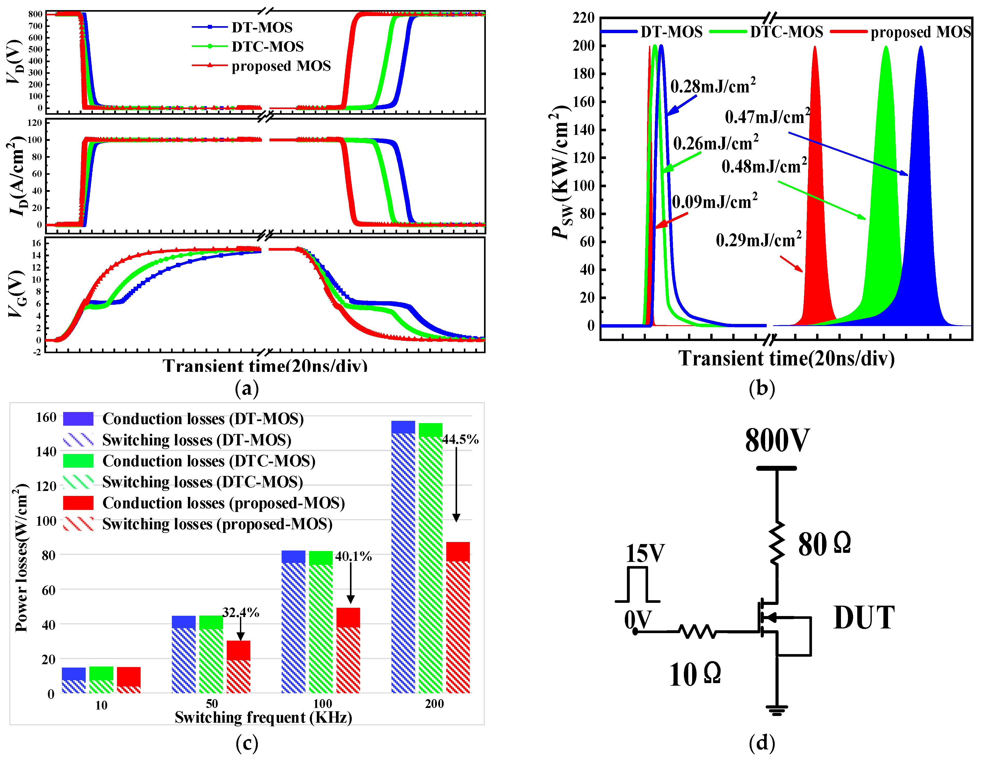
| Eon [mJ/cm2] | 0.28 | 0.26 | 0.09 |
| Eoff [mJ/cm2] | 0.47 | 0.48 | 0.29 |
Disclaimer/Publisher’s Note: The statements, opinions and data contained in all publications are solely those of the individual author(s) and contributor(s) and not of MDPI and/or the editor(s). MDPI and/or the editor(s) disclaim responsibility for any injury to people or property resulting from any ideas, methods, instructions or products referred to in the content. |
© 2024 by the authors. Licensee MDPI, Basel, Switzerland. This article is an open access article distributed under the terms and conditions of the Creative Commons Attribution (CC BY) license (https://creativecommons.org/licenses/by/4.0/).
Share and Cite
Ou, Y.; Lan, Z.; Hu, X.; Liu, D. Novel SiC Trench MOSFET with Improved Third-Quadrant Performance and Switching Speed. Micromachines 2024, 15, 254. https://doi.org/10.3390/mi15020254
Ou Y, Lan Z, Hu X, Liu D. Novel SiC Trench MOSFET with Improved Third-Quadrant Performance and Switching Speed. Micromachines. 2024; 15(2):254. https://doi.org/10.3390/mi15020254
Chicago/Turabian StyleOu, Yangjie, Zhong Lan, Xiarong Hu, and Dong Liu. 2024. "Novel SiC Trench MOSFET with Improved Third-Quadrant Performance and Switching Speed" Micromachines 15, no. 2: 254. https://doi.org/10.3390/mi15020254
APA StyleOu, Y., Lan, Z., Hu, X., & Liu, D. (2024). Novel SiC Trench MOSFET with Improved Third-Quadrant Performance and Switching Speed. Micromachines, 15(2), 254. https://doi.org/10.3390/mi15020254