

In Situ Pre-Metallization Cleaning of CoSi2 Contact-Hole Patterns with Optimized Etching Process


Abstract
1. Introduction
2. Materials and Methods
3. Results and Discussion
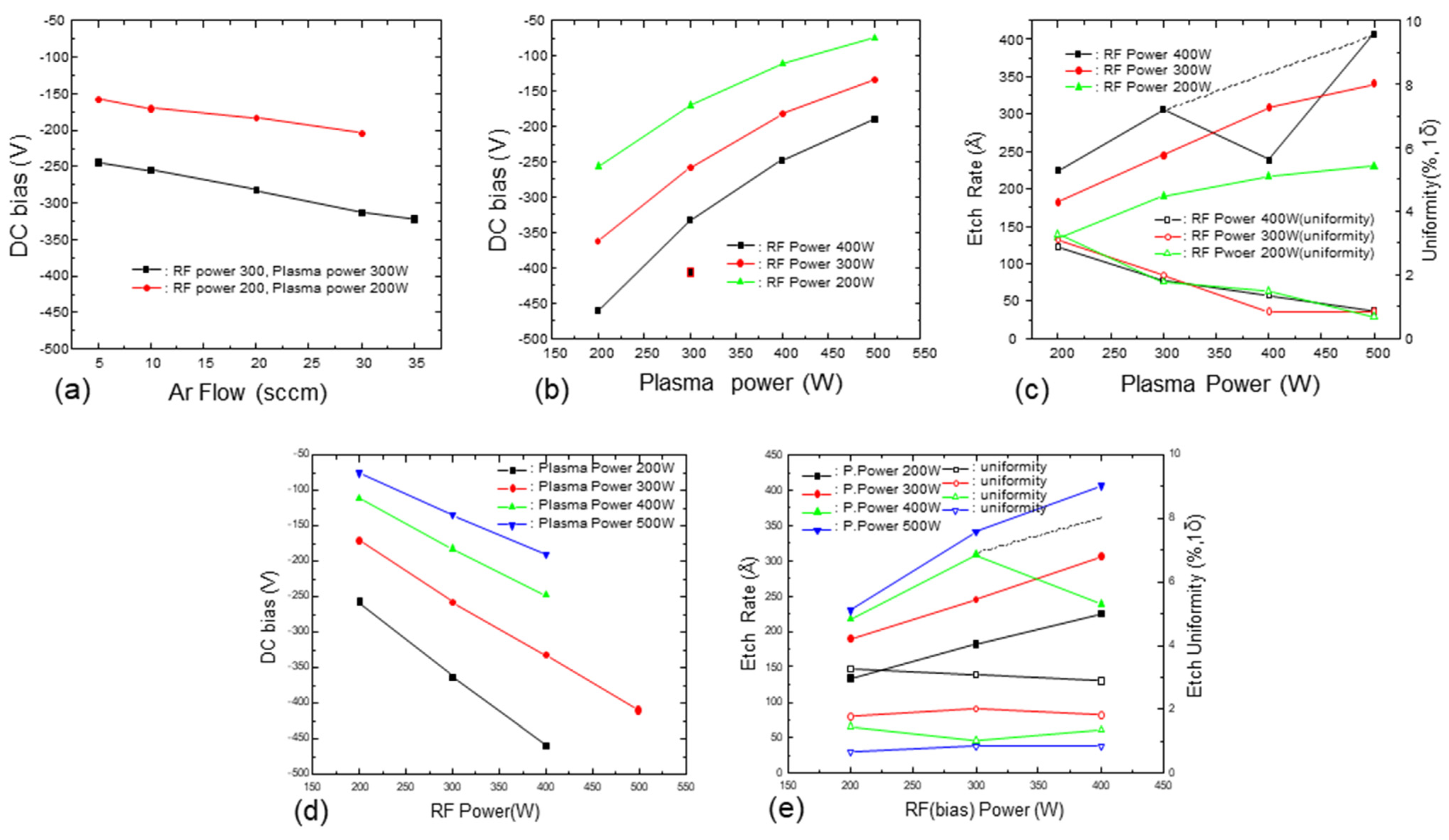
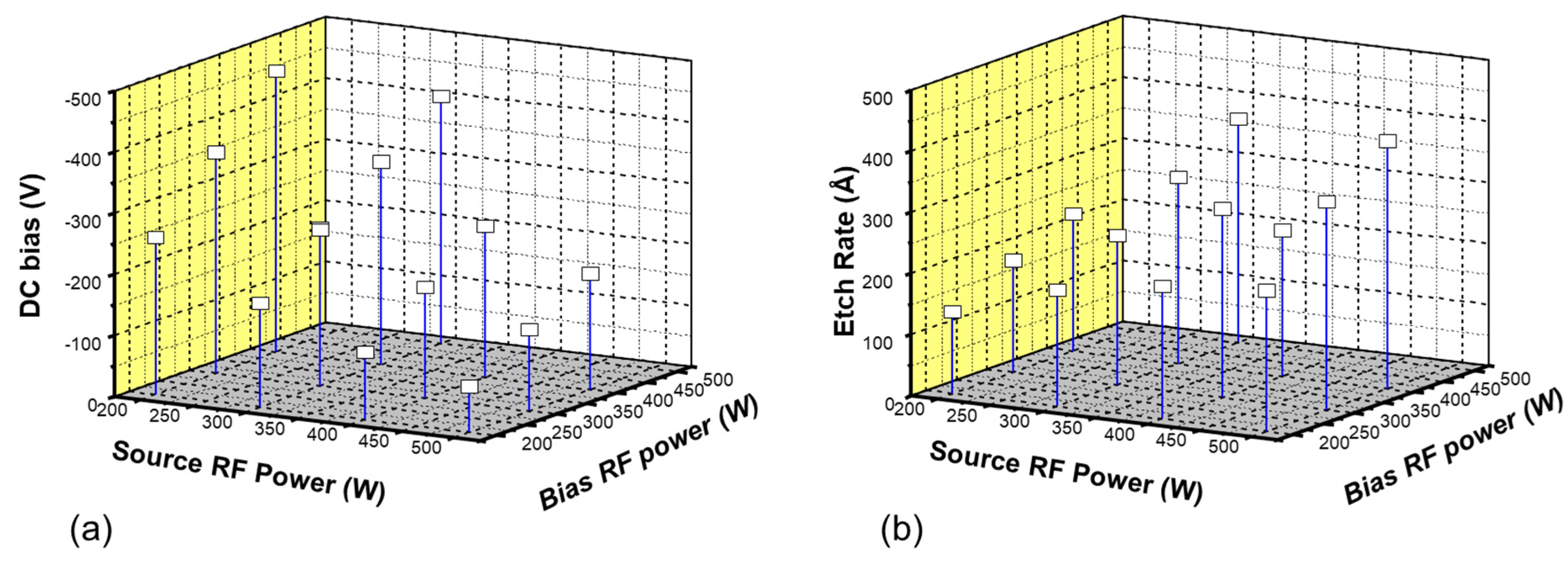
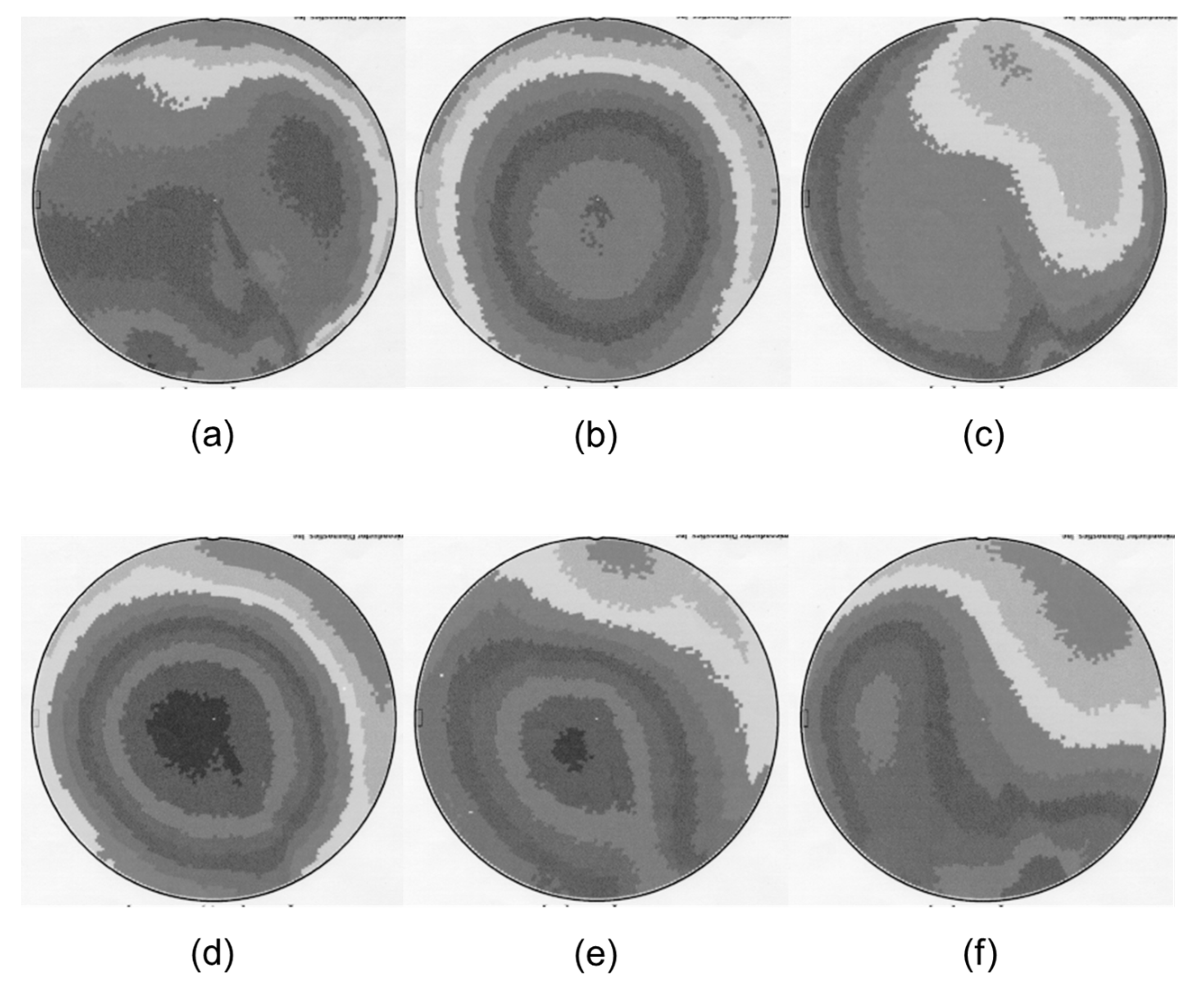
3.1. Chamber System Testing
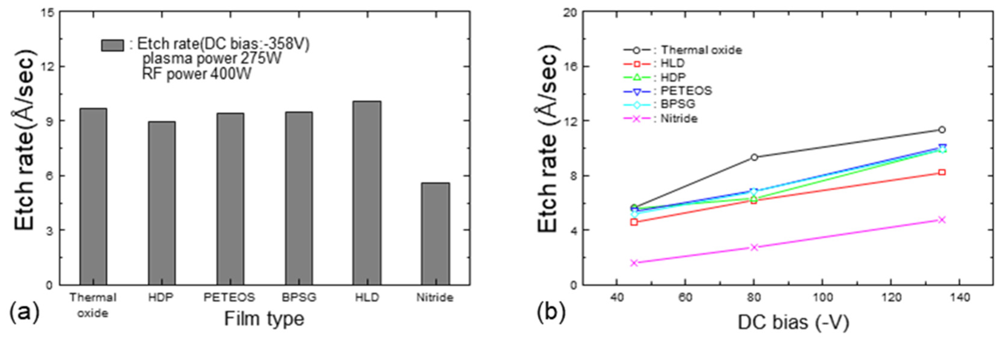
3.2. Etching of Various Oxide Layer Types
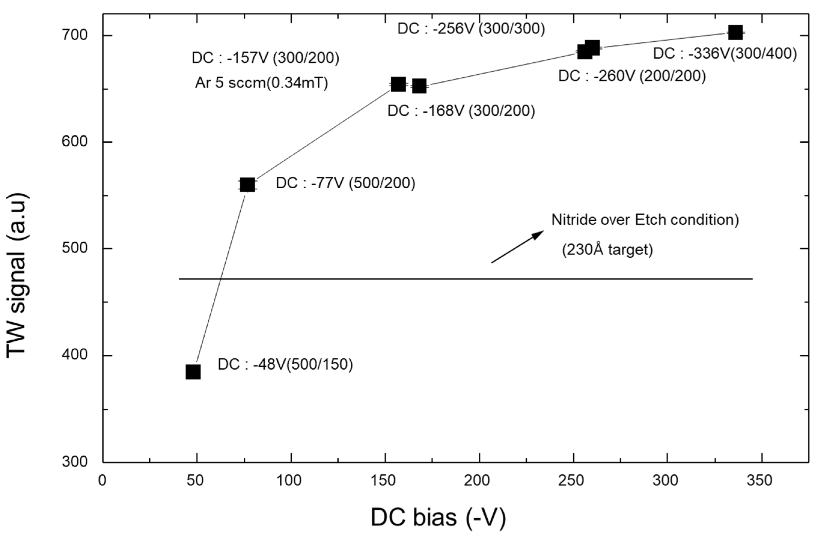
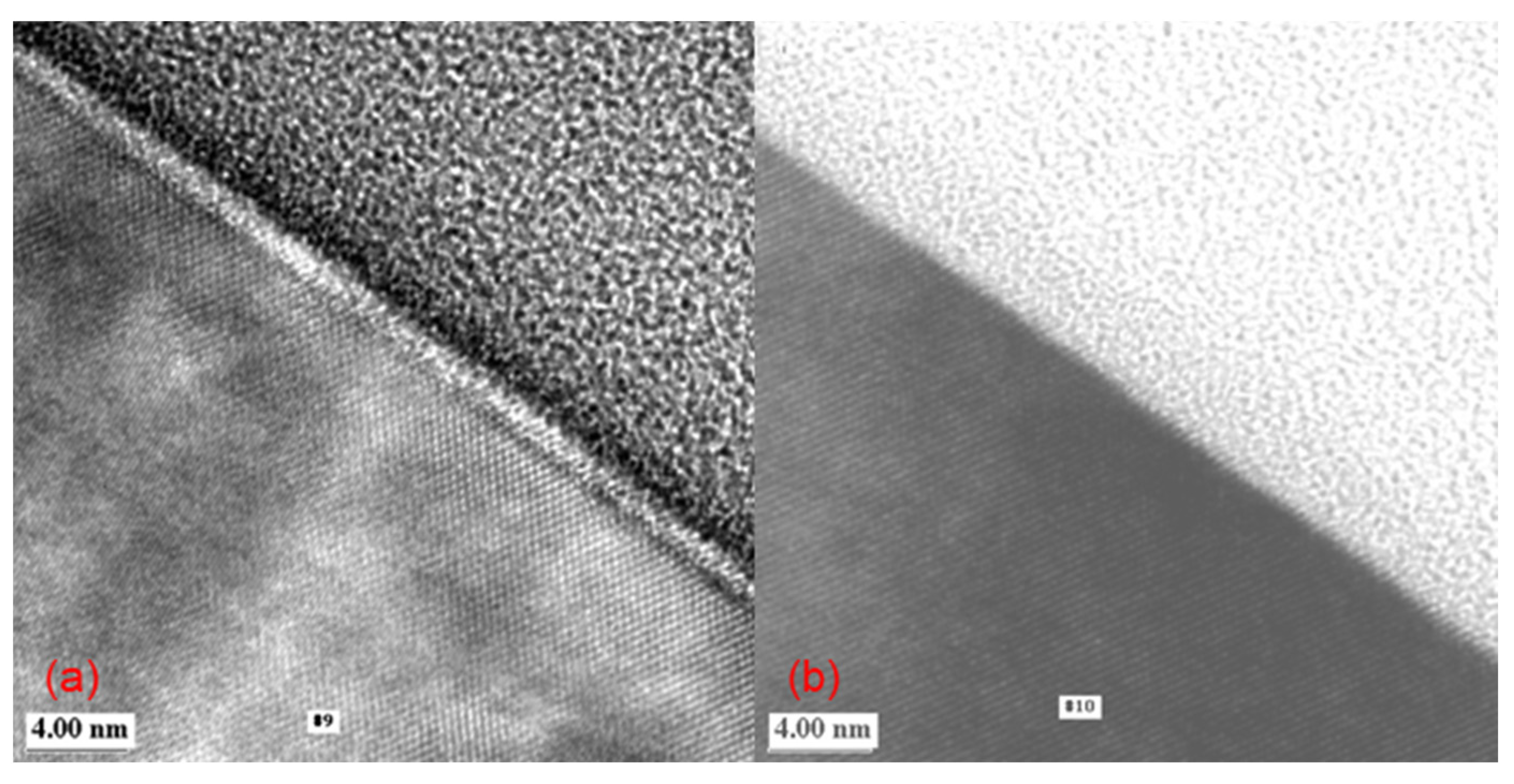
3.3. Damage Analysis
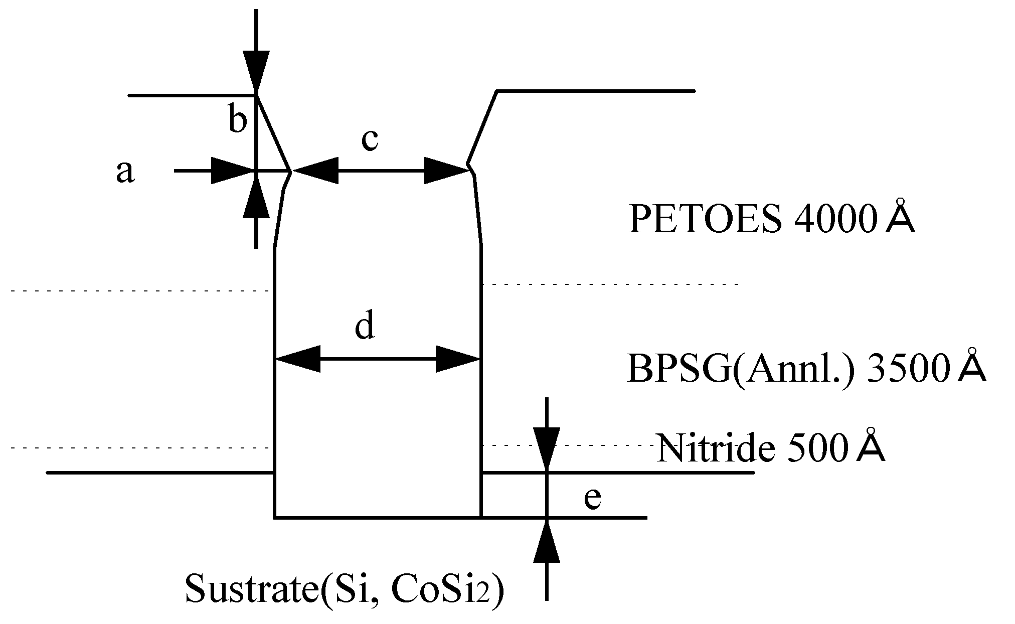
3.4. Sub-Layer Removal and Contact Profile Changes
4. Conclusions
Author Contributions
Funding
Data Availability Statement
Acknowledgments
Conflicts of Interest
References
- Vos, R.; Wada, M.; Arnauts, S.; Takahashi, H.; Cuypers, D.; Struyf, H.; Mertens, P. Cleaning aspects of novel materials after CMP. ECS Trans. 2011, 34, 671. [Google Scholar] [CrossRef]
- Beyer, K.; Kastl, R. Impact of deionized water rinses on silicon surface cleaning. J. Electrochem. Soc. 1982, 129, 1027. [Google Scholar] [CrossRef]
- Chen, C.; Jiang, L.; Zhang, P.; Wang, H.; Qian, L. Simple method to measure the etching rate of monocrystalline silicon in KOH solution. Micro Nano Lett. 2018, 13, 481–485. [Google Scholar] [CrossRef]
- Vos, I.; Hellin, D.; Vereecke, G.; Pavel, E.; Boullart, W.; Vertommen, J. Effect of etch-clean delay time on post-etch residue removal for front-end-of-line applications. J. Vac. Sci. Technol. B 2009, 27, 2301–2308. [Google Scholar] [CrossRef]
- Sayed, S.Y.; Wang, F.; Malac, M.; Meldrum, A.; Egerton, R.F.; Buriak, J.M. Heteroepitaxial growth of gold nanostructures on silicon by galvanic displacement. ACS Nano 2009, 3, 2809–2817. [Google Scholar] [CrossRef]
- Morita, M.; Ohmi, T.; Hasegawa, E.; Kawakami, M.; Ohwada, M. Growth of native oxide on a silicon surface. J. Appl. Phys. 1990, 68, 1272–1281. [Google Scholar] [CrossRef]
- Zhang, Y.; Loh, J.Y.; Flood, A.G.; Mao, C.; Sharma, G.; Kherani, N.P. Ultra-Sensitive Cubic-ITO/Silicon Photodiode via Interface Engineering of Native SiOx and Lattice-Strain-Assisted Atomic Oxidation. Adv. Funct. Mater. 2022, 32, 2109794. [Google Scholar] [CrossRef]
- Kurhekar, A.S.; Apte, P.R. Spectroscopic-ellipsometric study of native oxide removal by liquid phase HF process. Int. Nano Lett. 2013, 3, 1–9. [Google Scholar] [CrossRef]
- Juodkazis, K.; Juodkazytė, J.; Šebeka, B.; Savickaja, I.; Juodkazis, S. Photoelectrochemistry of silicon in HF solution. J. Solid State Electrochem. 2013, 17, 2269–2276. [Google Scholar] [CrossRef]
- Chen, H.-W.; Gouk, R.; Verhaverbeke, S.; Visser, R.J. Non-Stiction Performance of Various Post Wet-Clean Drying Schemes on High-Aspect-Ratio Device Structures. ECS Trans. 2013, 58, 205. [Google Scholar] [CrossRef]
- Yang, C.C.; Ko, C.C.; Yang, H.O.; Chen, K.F.; Peng, Y.Y.; Liou, J.W.; Chou, C.C.; Tsai, H.Y.; Lin, K.C.; Jeng, S.M.; et al. Wet Clean Induce Pattern Collapse Mechanism Study. Solid State Phenom. 2012, 187, 253–256. [Google Scholar] [CrossRef]
- Baklanov, M.R.; Kondoh, E.; Donaton, R.A.; Vanhaelemeersch, S.; Maex, K. Limitation of HF-Based Chemistry for Deep-Submicron Contact Hole Cleaning on Silicides. J. Electrochem. Soc. 1998, 145, 3240. [Google Scholar] [CrossRef]
- Lehmann, H.W.; Widmer, R. Profile control by reactive sputter etching. J. Vac. Sci. Technol. 1978, 15, 319–326. [Google Scholar] [CrossRef]
- Mikhailenko, M.S.; Pestov, A.E.; Chkhalo, N.I.; Zorina, M.V.; Chernyshev, A.K.; Salashchenko, N.N.; Kuznetsov, I.I. Influence of ion-beam etching by Ar ions with an energy of 200–1000 eV on the roughness and sputtering yield of a single-crystal silicon surface. Appl. Opt. 2022, 61, 2825–2833. [Google Scholar] [CrossRef]
- Gupta, V.; Madaan, N.; Jensen, D.S.; Kunzler, S.C.; Linford, M.R. Hydrogen Plasma Treatment of Silicon Dioxide for Improved Silane Deposition. Langmuir 2013, 29, 3604–3609. [Google Scholar] [CrossRef]
- Williams, T.S.; Hicks, R.F. Aging mechanism of the native oxide on silicon (100) following atmospheric oxygen plasma cleaning. J. Vac. Sci. Technol. A 2011, 29, 041403. [Google Scholar] [CrossRef]
- Aronsson, B.-O.; Lausmaa, J.; Kasemo, B. Glow discharge plasma treatment for surface cleaning and modification of metallic biomaterials. J. Biomed. Mater. Res. 1997, 35, 49–73. [Google Scholar] [CrossRef]
- Vossen, J.L. The preparation of substrates for film deposition using glow discharge techniques. J. Phys. E Sci. Instrum. 1979, 12, 159. [Google Scholar] [CrossRef]
- Mittal, K.L. Surface Contamination: An Overview. In Surface Contamination: Genesis, Detection, and Control; Mittal, K.L., Ed.; Springer: Boston, MA, USA, 1979; pp. 3–45. [Google Scholar] [CrossRef]
- Grégoire, M.; Horvat, B.; Bozon, B.N.; Combe, D.; Dabertrand, K.; Roy, D. Additional Siconi™ pre-clean for reliable TiSix contacts in advanced imager technologies. Micro Nano Eng. 2019, 2, 104–109. [Google Scholar] [CrossRef]
- Shiyang, Z.; Detavernier, C.; Meirhaeghe, R.L.V.; Cardon, F.; Blondeel, A.; Clauws, P.; Guo-Ping, R.; Bing-Zong, L. Electrical characterization of Ar-ion-bombardment-induced damage in Au/Si and PtSi/Si Schottky barrier contacts. Semicond. Sci. Technol. 2001, 16, 83. [Google Scholar] [CrossRef]
- Maex, K. Silicides for integrated circuits: TiSi2 CoSi2. Mater. Sci. Eng. R Rep. 1993, 11, vii-153. [Google Scholar] [CrossRef]
- Romanyuk, O.; Gordeev, I.; Paszuk, A.; Supplie, O.; Stoeckmann, J.P.; Houdkova, J.; Ukraintsev, E.; Bartoš, I.; Jiříček, P.; Hannappel, T. GaP/Si(0 0 1) interface study by XPS in combination with Ar gas cluster ion beam sputtering. Appl. Surf. Sci. 2020, 514, 145903. [Google Scholar] [CrossRef]
- Yew, T.R.; Reif, R. Low-temperature in situ surface cleaning of oxide-patterned wafers by Ar/H2 plasma sputter. J. Appl. Phys. 1990, 68, 4681–4693. [Google Scholar] [CrossRef]
- Godyak, V.A.; Piejak, R.B.; Alexandrovich, B.M. Electron energy distribution function measurements and plasma parameters in inductively coupled argon plasma. Plasma Sources Sci. Technol. 2002, 11, 525. [Google Scholar] [CrossRef]
- Pu, Y. Plasma Etch Equipment. In Handbook of Integrated Circuit Industry; Wang, Y., Chi, M.-H., Lou, J.J.-C., Chen, C.-Z., Eds.; Springer: Singapore, 2024; pp. 1441–1493. [Google Scholar] [CrossRef]
- Todorov, S.S.; Fossum, E.R. Sputtering of silicon dioxide near threshold. Appl. Phys. Lett. 1988, 52, 365–367. [Google Scholar] [CrossRef]
- Lee, Y.H. Surface damage threshold of Si and SiO2 in electron-cyclotron-resonance plasmas. J. Vac. Sci. Technol. A 1992, 10, 1318–1324. [Google Scholar] [CrossRef]
- Smentkowski, V.S. Trends in sputtering. Prog. Surf. Sci. 2000, 64, 1–58. [Google Scholar] [CrossRef]
- Yamada, N. Kinetic energy discrimination in collision/reaction cell ICP-MS: Theoretical review of principles and limitations. Spectrochim. Acta Part B At. Spectrosc. 2015, 110, 31–44. [Google Scholar] [CrossRef]
- Kushner, M.J. Monte-Carlo simulation of electron properties in rf parallel plate capacitively coupled discharges. J. Appl. Phys. 1983, 54, 4958–4965. [Google Scholar] [CrossRef]
- Yabumoto, N.; Oshima, M.; Michikami, O.; Yoshii, S. Surface Damage on Si Substrates Caused by Reactive Sputter Etching. Jpn. J. Appl. Phys. 1981, 20, 893. [Google Scholar] [CrossRef]
- Eriguchi, K. Characterization techniques of ion bombardment damage on electronic devices during plasma processing—Plasma process-induced damage. Jpn. J. Appl. Phys. 2021, 60, 040101. [Google Scholar] [CrossRef]


| Plasma Power (W) * | RF Power (W) † | Ar Flow Rate (sccm) | Pressure (mtorr) | DC Bias (V) | Etching Amount (Å)/Uniformity (%) |
|---|---|---|---|---|---|
| 300 | 500 | 10 | 0.68 | −404 | 366.21/1.83 |
| 200 | 400 | 10 | 0.68 | −460 | 224.88/2.89 |
| 300 | 400 | 10 | 0.68 | −332 | 306.29/1.82 |
| 400 | 400 | 10 | 0.68 | −247 | 238.79/1.36 |
| 500 | 400 | 10 | 0.68 | −190 | 406.23/0.86 |
| 200 | 300 | 10 | 0.68 | −362 | 182.55/3.10 |
| 300 | 300 | 10 | 0.68 | −258 | 245.31/2.01 |
| 400 | 300 | 10 | 0.68 | −182 | 308.92/0.85 |
| 500 | 300 | 10 | 0.68 | −134 | 340.90/0.85 |
| 200 | 200 | 10 | 0.68 | −257 | 134.00/3.28 |
| 300 | 200 | 10 | 0.68 | −170 | 190.19/1.78 |
| 400 | 200 | 10 | 0.68 | −111 | 217.28/1.48 |
| 500 | 200 | 10 | 0.68 | −75 | 230.48/0.68 |
| 500 | 150 | 10 | 0.68 | −45 | 168.90/0.00 |
| 300 | 300 | 5 | 0.35 | −244 | - |
| 300 | 300 | 10 | 0.68 | −255 | - |
| 300 | 300 | 20 | 1.36 | −282 | - |
| 300 | 300 | 30 | 2.05 | −313 | 220.57/7.56 |
| 300 | 300 | 35 | 2.35 | −322 | - |
| 500 | 300 | 30 | 2.05 | −146 | 300.00/4.06 |
| 300 | 400 | 30 | 2.06 | −398 | 272.20/6.52 |
| 300 | 200 | 5 | 0.31 | −158 | 185.97/1.55 |
| 300 | 200 | 20 | 1.36 | −183 | 169.79/4.32 |
| 300 | 200 | 30 | 2.03 | −204 | 154.76/7.52 |
| Wafer # | a | b | c | d | e | CoSi2 Layer Etching Amount | b/a | d/c |
|---|---|---|---|---|---|---|---|---|
| 1 | 800 | 1570 | 2870 | 3200 | 900 (630) | All + Si 300 | 1.95 | 1.11 |
| 2 | 600 | 1600 | 2970 | 3230 | 370 (100) | All | 2.67 | 1.09 |
| 3 | 730 | 1370 | 2970 | 3230 | 400 (130) | All + Si 70 | 1.86 | 1.09 |
| 4 | 800 | 1330 | 3070 | 3300 | 400 (130) | All + Si 30 | 1.67 | 1.08 |
| 5 | 730 | 1230 | 2670 | 2930 | 330 (70) | 200 | 1.68 | 1.10 |
| 6 | 800 | 1200 | 2800 | 3070 | 270 (0) | 100 | 1.5 | 1.09 |
| 7 | – | – | 3130 | 3340 | 270 | 70 | – | 1.06 |
| Wafer # | Plasma Power (W) | RF Power (W) | DC Bias (V) | Si Etching Rate (Å/s) | CoSi2 Etching Rate (Å/s) |
|---|---|---|---|---|---|
| 1 | 300 | 400 | −334 | 31.7 | Etching off + Si loss |
| 2 | 300 | 300 | −256 | 4.0 | Etching off |
| 3 | 300 | 200 | −172 | 4.2 | Etching off + Si loss |
| 4 | 200 | 200 | −265 | 2.9 | Etching off |
| 5 | 500 | 200 | −78 | 2.5 | 5.11 |
| 6 | 500 | 150 | −50 | 0 | 0.94 |
Disclaimer/Publisher’s Note: The statements, opinions and data contained in all publications are solely those of the individual author(s) and contributor(s) and not of MDPI and/or the editor(s). MDPI and/or the editor(s) disclaim responsibility for any injury to people or property resulting from any ideas, methods, instructions or products referred to in the content. |
© 2024 by the authors. Licensee MDPI, Basel, Switzerland. This article is an open access article distributed under the terms and conditions of the Creative Commons Attribution (CC BY) license (https://creativecommons.org/licenses/by/4.0/).
Share and Cite
Choi, T.-M.; Jung, E.-S.; Yoo, J.-U.; Lee, H.-R.; Yoon, S.; Pyo, S.-G. In Situ Pre-Metallization Cleaning of CoSi2 Contact-Hole Patterns with Optimized Etching Process. Micromachines 2024, 15, 1409. https://doi.org/10.3390/mi15121409
Choi T-M, Jung E-S, Yoo J-U, Lee H-R, Yoon S, Pyo S-G. In Situ Pre-Metallization Cleaning of CoSi2 Contact-Hole Patterns with Optimized Etching Process. Micromachines. 2024; 15(12):1409. https://doi.org/10.3390/mi15121409
Chicago/Turabian StyleChoi, Tae-Min, Eun-Su Jung, Jin-Uk Yoo, Hwa-Rim Lee, Songhun Yoon, and Sung-Gyu Pyo. 2024. "In Situ Pre-Metallization Cleaning of CoSi2 Contact-Hole Patterns with Optimized Etching Process" Micromachines 15, no. 12: 1409. https://doi.org/10.3390/mi15121409
APA StyleChoi, T.-M., Jung, E.-S., Yoo, J.-U., Lee, H.-R., Yoon, S., & Pyo, S.-G. (2024). In Situ Pre-Metallization Cleaning of CoSi2 Contact-Hole Patterns with Optimized Etching Process. Micromachines, 15(12), 1409. https://doi.org/10.3390/mi15121409