
The Understanding and Compact Modeling of Reliability in Modern Metal–Oxide–Semiconductor Field-Effect Transistors: From Single-Mode to Mixed-Mode Mechanisms


Abstract
1. Introduction
2. Mixed-Mode Reliability Mechanisms
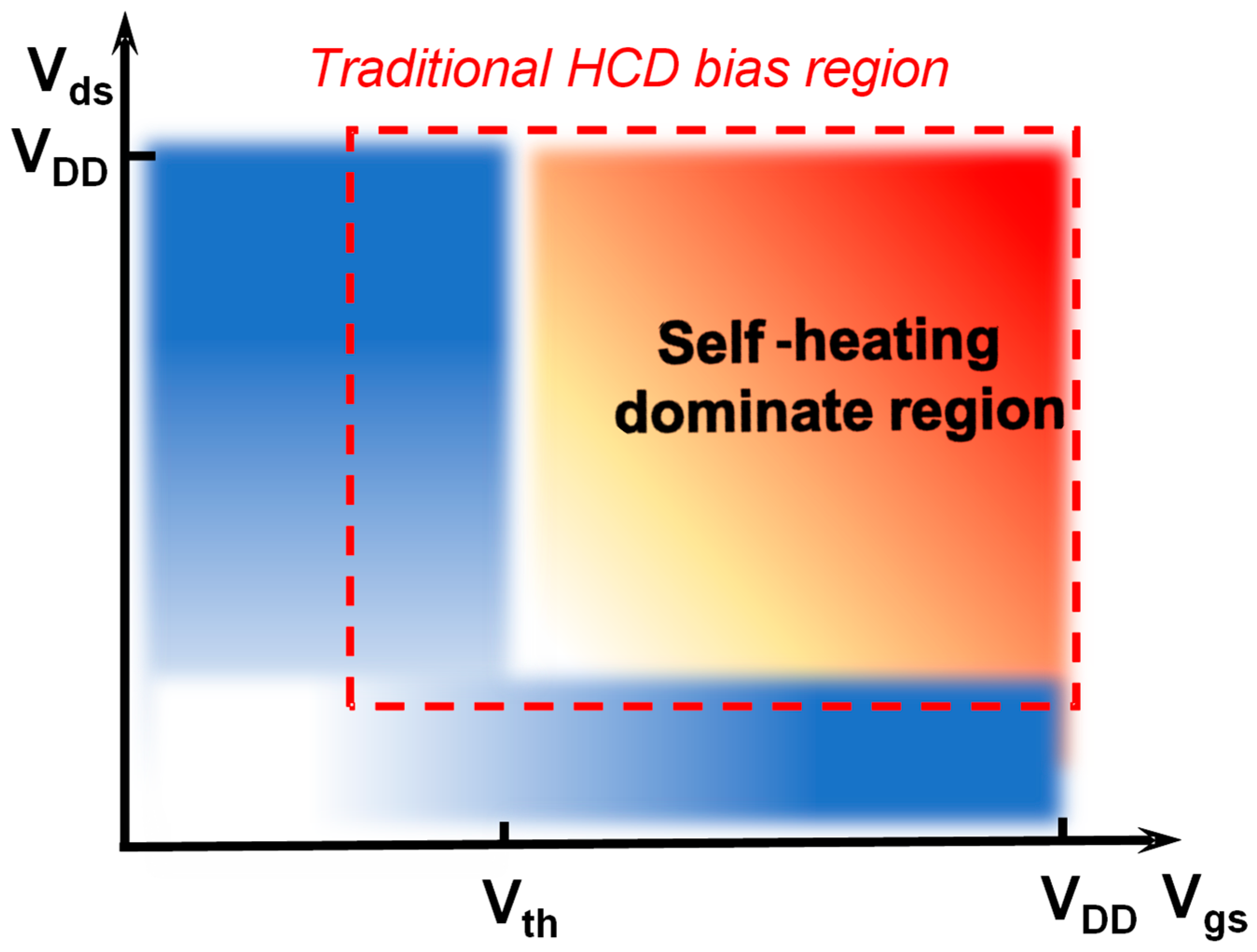
2.1. Hot Carrier Degradation with Self-Heating Effect
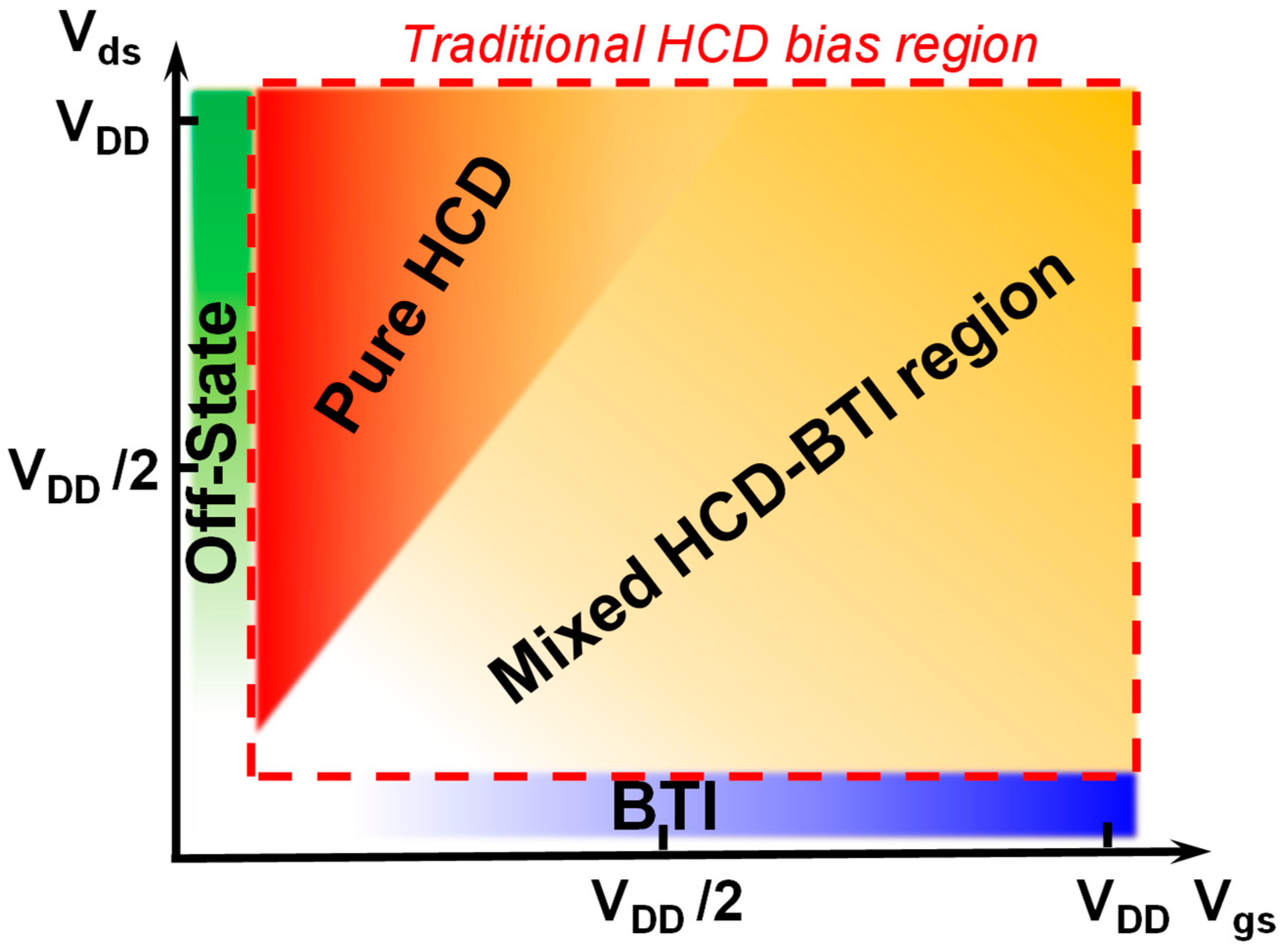
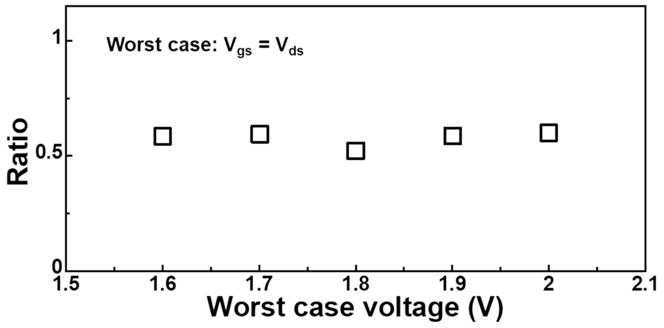
2.2. Hot Carrier Degradation with Inhomogeneous Bias Temperature Instability
2.3. Mechanisms in Off-State Degradation
2.4. On-State Time-Dependent Dielectric Breakdown with Self-Heating Effect
2.5. Gate Metal Electromigration with On-State Soft Breakdown
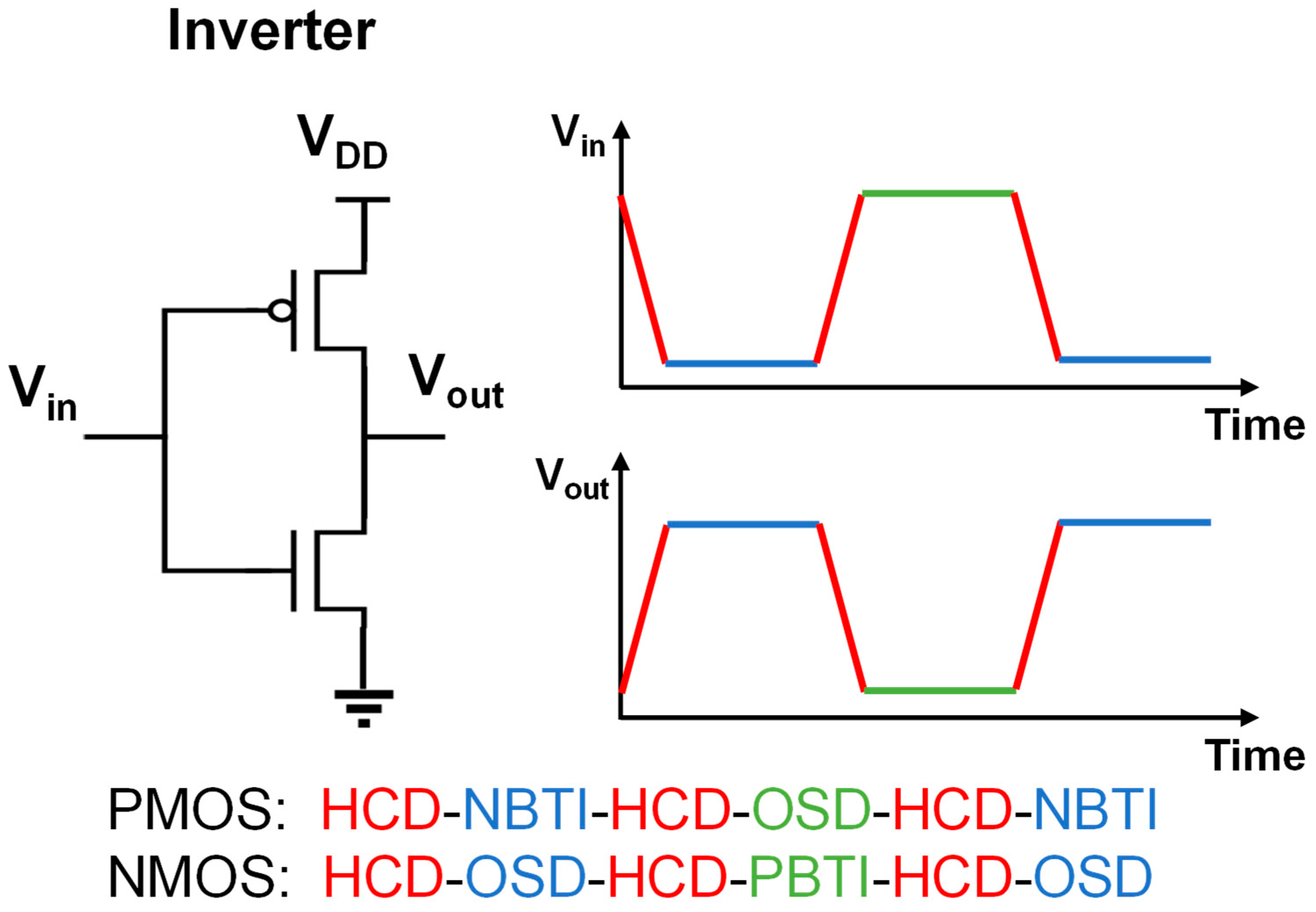
3. Impact of Alternating Stress Conditions
4. Conclusions
Author Contributions
Funding
Data Availability Statement
Conflicts of Interest
References
- Falcony, C.; Aguilar-Frutis, M.A.; García-Hipólito, M. Spray Pyrolysis Technique; High-K Dielectric Films and Luminescent Materials: A Review. Micromachines 2018, 9, 414. [Google Scholar] [CrossRef]
- Wu, C.; Lin, D.; Keshavarzi, A.; Huang, C.; Chan, C.; Tseng, C.; Chen, C.; Hsieh, C.; Wong, K.; Cheng, M.; et al. High Performance 22/20nm FinFET CMOS Devices with Advanced High-K/Metal Gate Scheme. In Proceedings of the 2010 International Electron Devices Meeting, San Francisco, CA, USA, 6–8 December 2010; IEEE: Piscataway, NJ, USA, 2010; pp. 27.1.1–27.1.4. [Google Scholar]
- Smith, C.; Adhikari, H.; Lee, S.; Coss, B.; Parthasarathy, S.; Young, C.; Sassman, B.; Cruz, M.; Hobbs, C.; Majhi, P.; et al. Dual Channel FinFETs as a Single High-k/Metal Gate Solution beyond 22nm Node. In Proceedings of the 2009 IEEE International Electron Devices Meeting (IEDM), Baltimore, MD, USA, 7–9 December 2009; IEEE: Piscataway, NJ, USA, 2009; pp. 1–4. [Google Scholar]
- Yeh, C.-C.; Chang, C.-S.; Lin, H.-N.; Tseng, W.-H.; Lai, L.-S.; Perng, T.-H.; Lee, T.-L.; Chang, C.-Y.; Yao, L.-G.; Chen, C.-C.; et al. A Low Operating Power FinFET Transistor Module Featuring Scaled Gate Stack and Strain Engineering for 32/28 nm SoC Technology. In Proceedings of the 2010 International Electron Devices Meeting, San Francisco, CA, USA, 6–8 December 2010; IEEE: Piscataway, NJ, USA, 2010; pp. 34.1.1–34.1.4. [Google Scholar]
- Lee, C.-C.; Huang, P.-C.; Hsiang, T.-P. Interactive Lattice and Process-Stress Responses in the Sub-7 Nm Germanium-Based Three-Dimensional Transistor Architecture of FinFET and Nanowire GAAFET. IEEE Trans. Electron Devices 2022, 69, 6552–6560. [Google Scholar] [CrossRef]
- Schmidt, M.; Süess, M.J.; Barros, A.D.; Geiger, R.; Sigg, H.; Spolenak, R.; Minamisawa, R.A. A Patterning-Based Strain Engineering for Sub-22 nm Node FinFETs. IEEE Electron Device Lett. 2014, 35, 300–302. [Google Scholar] [CrossRef]
- Collaert, N.; De Keersgieter, A.; Dixit, A.; Ferain, I.; Lai, L.-S.; Lenoble, D.; Mercha, A.; Nackaerts, A.; Pawlak, B.; Rooyackers, R.; et al. Multi-Gate Devices for the 32 nm Technology Node and Beyond. Solid-State Electron. 2008, 52, 1291–1296. [Google Scholar] [CrossRef]
- Bughio, A.M.; Guerrieri, S.D.; Bonani, F.; Ghione, G. Multi-Gate FinFET Mixer Variability Assessment through Physics-Based Simulation. IEEE Electron Device Lett. 2017, 38, 1004–1007. [Google Scholar] [CrossRef]
- Inaba, S.; Okano, K.; Izumida, T.; Kaneko, A.; Kawasaki, H.; Yagishita, A.; Kanemura, T.; Ishida, T.; Aoki, N.; Ishimaru, K.; et al. FinFET: The Prospective Multi-Gate Device for Future SoC Applications. In Proceedings of the 2006 European Solid-State Device Research Conference, Montreux, Switzerland, 19–21 September 2006; IEEE: Piscataway, NJ, USA, 2006; pp. 49–52. [Google Scholar]
- Leonelli, D.; Vandooren, A.; Rooyackers, R.; Verhulst, A.S.; De Gendt, S.; Heyns, M.M.; Groeseneken, G. Performance Enhancement in Multi Gate Tunneling Field Effect Transistors by Scaling the Fin-Width. Jpn. J. Appl. Phys. 2010, 49, 04DC10. [Google Scholar] [CrossRef]
- Chen, S.; Jiao, Y.; Peng, B.; Li, M.; Zhang, L.; Wang, R.; Huang, R. Thermal Evaluation for Monolithic 3D Integrated Circuits Based on Gate-All-Around Transistors. In Proceedings of the 2023 International Symposium of Electronics Design Automation (ISEDA), Nanjing, China, 8–11 May 2023; IEEE: Piscataway, NJ, USA, 2023; pp. 418–422. [Google Scholar]
- Goel, A.; Rawat, A.; Rawat, B. Benchmarking of Analog/RF Performance of Fin-FET, NW-FET, and NS-FET in the Ultimate Scaling Limit. IEEE Trans. Electron Devices 2022, 69, 1298–1305. [Google Scholar] [CrossRef]
- Loubet, N.; Hook, T.; Montanini, P.; Yeung, C.-W.; Kanakasabapathy, S.; Guillom, M.; Yamashita, T.; Zhang, J.; Miao, X.; Wang, J.; et al. Stacked Nanosheet Gate-All-around Transistor to Enable Scaling beyond FinFET. In Proceedings of the 2017 Symposium on VLSI Technology, Kyoto, Japan, 5–8 June 2017; IEEE: Piscataway, NJ, USA, 2017; pp. T230–T231. [Google Scholar]
- Cao, W.; Bu, H.; Vinet, M.; Cao, M.; Takagi, S.; Hwang, S.; Ghani, T.; Banerjee, K. The Future Transistors. Nature 2023, 620, 501–515. [Google Scholar] [CrossRef]
- Radamson, H.H.; He, X.; Zhang, Q.; Liu, J.; Cui, H.; Xiang, J.; Kong, Z.; Xiong, W.; Li, J.; Gao, J.; et al. Miniaturization of CMOS. Micromachines 2019, 10, 293. [Google Scholar] [CrossRef] [PubMed]
- Radamson, H.H.; Zhu, H.; Wu, Z.; He, X.; Lin, H.; Liu, J.; Xiang, J.; Kong, Z.; Xiong, W.; Li, J.; et al. State of the Art and Future Perspectives in Advanced CMOS Technology. Nanomaterials 2020, 10, 1555. [Google Scholar] [CrossRef]
- Liu, C.; Sagong, H.-C.; Kim, H.; Choo, S.; Lee, H.; Kim, Y.; Kim, H.; Jo, B.; Jin, M.; Kim, J.; et al. Systematical Study of 14nm FinFET Reliability: From Device Level Stress to Product HTOL. In Proceedings of the 2015 IEEE International Reliability Physics Symposium, Monterey, CA, USA, 19–23 April 2015; IEEE: Piscataway, NJ, USA, 2015; pp. 2F.3.1–2F.3.5. [Google Scholar]
- Ji, Z.; Chen, H.; Li, X. Design for Reliability with the Advanced Integrated Circuit (IC) Technology: Challenges and Opportunities. Sci. China Inf. Sci. 2019, 62, 1–4. [Google Scholar] [CrossRef]
- Choi, Y.-K.; Ha, D.; Snow, E.; Bokor, J.; King, T.-J. Reliability Study of CMOS FinFETs. In Proceedings of the IEEE International Electron Devices Meeting 2003, Washington, DC, USA, 8–10 December 2003; IEEE: Piscataway, NJ, USA, 2003; pp. 7.6.1–7.6.4. [Google Scholar]
- Teng, Q.; Hu, Y.; Cheng, R.; Wu, Y.; Zhou, G.; Gao, D. Reliability Challenges in CMOS Technology: A Manufacturing Process Perspective. Microelectron. Eng. 2023, 281, 112086. [Google Scholar] [CrossRef]
- Huang, R.; Jiang, X.; Guo, S.; Ren, P.; Hao, P.; Yu, Z.; Zhang, Z.; Wang, Y.; Wang, R. Variability-and Reliability-Aware Design for 16/14nm and beyond Technology. In Proceedings of the 2017 IEEE International Electron Devices Meeting (IEDM), San Francisco, CA, USA, 2–6 December 2017; IEEE: Piscataway, NJ, USA, 2017; pp. 12–14. [Google Scholar]
- Jin, M.; Liu, C.; Kim, J.; Kim, J.; Shim, H.; Kim, K.; Kim, G.; Lee, S.; Uemura, T.; Chang, M.; et al. Reliability Characterization of 10nm FinFET Technology with Multi-V T Gate Stack for Low Power and High Performance. In Proceedings of the 2016 IEEE International Electron Devices Meeting (IEDM), San Francisco, CA, USA, 3–7 December 2016; IEEE: Piscataway, NJ, USA, 2016; pp. 15.1.1–15.1.4. [Google Scholar]
- Choi, K.; Sagong, H.C.; Jin, M.; Hai, J.; Lee, M.; Jeong, T.; Yeo, M.S.; Shim, H.; Ahn, D.; Kim, W.; et al. Reliability on Evolutionary FinFET CMOS Technology and Beyond. In Proceedings of the 2020 IEEE International Electron Devices Meeting (IEDM), San Francisco, CA, USA, 12–18 December 2020; IEEE: Piscataway, NJ, USA, 2020; pp. 9.3.1–9.3.4. [Google Scholar]
- Hsieh, E.; Wang, Z.; Ye, Y.; Wu, Y.; Huang, C.; Huang, P.; Huang, Y.; Miu, M.; Su, H.; Huang, S.; et al. Positive-Bias-Temperature-Instability Induced Random-Trap-Fluctuation Enhanced Physical Unclonable Functions on 14-Nm nFinFETs. IEEE Electron Device Lett. 2022, 43, 1396–1399. [Google Scholar] [CrossRef]
- Claes, D.; Franco, J.; Collaert, N.; Linten, D.; Heyns, M. Positive Bias Temperature Instability of HfO2-Based Gate Stacks at Reduced Thermal Budget for Future CMOS Technologies. J. Appl. Phys. 2020, 128, 104101. [Google Scholar] [CrossRef]
- Rzepa, G.; Franco, J.; Subirats, A.; Jech, M.; Chasin, A.; Grill, A.; Waltl, M.; Knobloch, T.; Stampfer, B.; Chiarella, T.; et al. Efficient Physical Defect Model Applied to PBTI in High-κ Stacks. In Proceedings of the 2017 IEEE International Reliability Physics Symposium (IRPS), Monterey, CA, USA, 2–6 April 2017; IEEE: Piscataway, NJ, USA, 2017; p. XT-11. [Google Scholar]
- Guo, S.; Wang, R.; Yu, Z.; Hao, P.; Ren, P.; Wang, Y.; Liao, S.; Huang, C.; Guo, T.; Chen, A.; et al. Towards Reliability-Aware Circuit Design in Nanoscale FinFET Technology:—New-Generation Aging Model and Circuit Reliability Simulator. In Proceedings of the 2017 IEEE/ACM International Conference on Computer-Aided Design (ICCAD), Irvine, CA, USA, 13–16 November 2017; IEEE: Piscataway, NJ, USA, 2017; pp. 780–785. [Google Scholar]
- Tyaginov, S.; O’Sullivan, B.; Chasin, A.; Rawal, Y.; Chiarella, T.; de Carvalho Cavalcante, C.T.; Kimura, Y.; Vandemaele, M.; Ritzenthaler, R.; Mitard, J.; et al. Impact of Nitridation on Bias Temperature Instability and Hard Breakdown Characteristics of SiON MOSFETs. Micromachines 2023, 14, 1514. [Google Scholar] [CrossRef]
- Li, Y.; Xue, Y.; Sun, Z.; Shen, C.; Ren, P.; Ji, Z.; Zhang, L.; Wang, R.; Huang, R. A Device-Circuit Aging Simulation Framework Integrating Trap-Based Models and Sensitivity Analysis for FinFET Technology. IEEE Trans. Electron Devices 2023, 71, 206–212. [Google Scholar] [CrossRef]
- Krishnan, A.T.; Reddy, V.; Chakravarthi, S.; Rodriguez, J.; John, S.; Krishnan, S. NBTI Impact on Transistor and Circuit: Models, Mechanisms and Scaling Effects [MOSFETs]. In Proceedings of the IEEE International Electron Devices Meeting 2003, Washington, DC, USA, 8–10 December 2003; IEEE: Piscataway, NJ, USA, 2003; pp. 14–15. [Google Scholar]
- Zhang, Z.; Wang, R.; Shen, X.; Wu, D.; Zhang, J.; Zhang, Z.; Wang, J.; Huang, R. Aging-Aware Gate-Level Modeling for Circuit Reliability Analysis. IEEE Trans. Electron Devices 2021, 68, 4201–4207. [Google Scholar] [CrossRef]
- Zhang, J.; Wang, Z.; Wang, R.; Sun, Z.; Huang, R. Body Bias Dependence of Bias Temperature Instability (BTI) in Bulk FinFET Technology. Energy Environ. Mater. 2022, 5, 1200–1203. [Google Scholar] [CrossRef]
- Ren, P.; Wang, R.; Ji, Z.; Hao, P.; Jiang, X.; Guo, S.; Luo, M.; Duan, M.; Zhang, J.F.; Wang, J.; et al. New Insights into the Design for End-of-Life Variability of NBTI in Scaled High-κ/Metal-Gate Technology for the Nano-Reliability Era. In Proceedings of the 2014 IEEE International Electron Devices Meeting, San Francisco, CA, USA, 15–17 December 2014; IEEE: Piscataway, NJ, USA, 2014; pp. 34.1.1–34.1.4. [Google Scholar]
- Sun, Z.; Yu, Z.; Zhang, Z.; Zhang, J.; Wang, R.; Lu, P.; Huang, R. Investigation on the Lateral Trap Distributions in Nanoscale MOSFETs during Hot Carrier Stress. IEEE Electron Device Lett. 2019, 40, 490–493. [Google Scholar] [CrossRef]
- Wang, Z.; Lu, H.; Sun, Z.; Shen, C.; Peng, B.; Li, W.; Xue, Y.; Wang, D.; Ji, Z.; Zhang, L.; et al. New Insights into the Interface Trap Generation during Hot Carrier Degradation: Impacts of Full-band Electronic Resonance, (100) vs. (110), and nMOS vs. pMOS. In Proceedings of the 2023 IEEE International Electron Devices Meeting, San Francisco, CA, USA, 9–13 December 2023. [Google Scholar]
- Tyaginov, S.; Bury, E.; Grill, A.; Yu, Z.; Makarov, A.; De Keersgieter, A.; Vexler, M.; Vandemaele, M.; Wang, R.; Spessot, A.; et al. Compact Physics Hot-Carrier Degradation Model Valid over a Wide Bias Range. Micromachines 2023, 14, 2018. [Google Scholar] [CrossRef]
- Wang, R.; Sun, Z.; Liu, Y.-Y.; Yu, Z.; Wang, Z.; Jiang, X.; Huang, R. Understanding Hot Carrier Reliability in FinFET Technology from Trap-Based Approach. In Proceedings of the 2021 IEEE International Electron Devices Meeting (IEDM), San Francisco, CA, USA, 11–16 December 2021; IEEE: Piscataway, NJ, USA, 2021; pp. 31–32. [Google Scholar]
- Yu, Z.; Zhang, J.; Wang, R.; Guo, S.; Liu, C.; Huang, R. New Insights into the Hot Carrier Degradation (HCD) in FinFET: New Observations, Unified Compact Model, and Impacts on Circuit Reliability. In Proceedings of the 2017 IEEE International Electron Devices Meeting (IEDM), San Francisco, CA, USA, 2–6 December 2017; IEEE: Piscataway, NJ, USA, 2017; pp. 7.2.1–7.2.4. [Google Scholar]
- Makarov, A.; Tyaginov, S.; Kaczer, B.; Jech, M.; Chasin, A.; Grill, A.; Hellings, G.; Vexler, M.; Linten, D.; Grasser, T. Hot-Carrier Degradation in FinFETs: Modeling, Peculiarities, and Impact of Device Topology. In Proceedings of the 2017 IEEE International Electron Devices Meeting (IEDM), San Francisco, CA, USA, 2–6 December 2017; IEEE: Piscataway, NJ, USA, 2017; pp. 13.1.1–13.1.4. [Google Scholar]
- Grasser, T. Hot Carrier Degradation in Semiconductor Devices; Springer: Cham, Switzerland, 2014. [Google Scholar]
- Yu, Z.; Zhang, Z.; Sun, Z.; Wang, R.; Huang, R. On the Trap Locations in Bulk finFETs after Hot Carrier Degradation (HCD). IEEE Trans. Electron Devices 2020, 67, 3005–3009. [Google Scholar] [CrossRef]
- Cho, M.; Spessot, A.; Kaczer, B.; Aoulaiche, M.; Ritzenthaler, R.; Schram, T.; Fazan, P.; Horiguchi, N.; Linten, D. Off-State Stress Degradation Mechanism on Advanced p-MOSFETs. In Proceedings of the 2015 International Conference on IC Design & Technology (ICICDT), Leuven, Belgium, 1–3 June 2015; IEEE: Piscataway, NJ, USA, 2015; pp. 1–4. [Google Scholar]
- Crespo-Yepes, A.; Nasarre, C.; Garsot, N.; Martin-Martinez, J.; Rodriguez, R.; Barajas, E.; Aragones, X.; Mateo, D.; Nafria, M. CMOS Inverter Performance Degradation and Its Correlation with BTI, HCI and OFF State MOSFETs Aging. Solid-State Electron. 2022, 191, 108264. [Google Scholar] [CrossRef]
- Sun, Z.; Cai, P.; Song, J.; Wang, D.; Liu, Z.; Zhou, L.; Zhu, T.; Xue, Y.; Liu, Y.; Wang, Z.; et al. Comprehensive Study of NBTI and Off-State Reliabilty in Sub-20 nm DRAM Technology: Trap Identification, Compact Aging Model, and Impact on Retention Degradation. In Proceedings of the 2023 IEEE International Electron Devices Meeting, San Francisco, CA, USA, 9–13 December 2023. [Google Scholar]
- Kim, H.; Jin, M.; Sagong, H.; Kim, J.; Jung, U.; Choi, M.; Park, J.; Shin, S.; Pae, S. A Systematic Study of Gate Dielectric TDDB in FinFET Technology. In Proceedings of the 2018 IEEE International Reliability Physics Symposium (IRPS), Burlingame, CA, USA, 11–15 March 2018; IEEE: Piscataway, NJ, USA, 2018; pp. 4A.4-1–4A.4-4. [Google Scholar]
- Yang, K.; Liu, T.; Zhang, R.; Milor, L. A Comprehensive Time-Dependent Dielectric Breakdown Lifetime Simulator for Both Traditional CMOS and FinFET Technology. IEEE Trans. Very Large Scale Integr. (VLSI) Syst. 2018, 26, 2470–2482. [Google Scholar] [CrossRef]
- Wu, E.Y. Facts and Myths of Dielectric Breakdown Processes—Part I: Statistics, Experimental, and Physical Acceleration Models. IEEE Trans. Electron Devices 2019, 66, 4523–4534. [Google Scholar] [CrossRef]
- Pierce, D.; Brusius, P. Electromigration: A Review. Microelectron. Reliab. 1997, 37, 1053–1072. [Google Scholar] [CrossRef]
- Zahedmanesh, H.; Ciofi, I.; Zografos, O.; Croes, K.; Badaroglu, M. System-Level Simulation of Electromigration in a 3 nm Cmos Power Delivery Network: The Effect of Grid Redundancy, Metallization Stack and Standard-Cell Currents. In Proceedings of the 2022 IEEE International Reliability Physics Symposium (IRPS), Dallas, TX, USA, 27–31 March 2022; IEEE: Piscataway, NJ, USA, 2022; pp. 1–7. [Google Scholar]
- Arnaud, L.; Lamontagne, P.; Galand, R.; Petitprez, E.; Ney, D.; Waltz, P. Electromigration Induced Void Kinetics in Cu Interconnects for Advanced CMOS Nodes. In Proceedings of the 2011 International Reliability Physics Symposium, Monterey, CA, USA, 10–14 April 2011; IEEE: Piscataway, NJ, USA, 2011; pp. 3E.1.1–3E.1.10. [Google Scholar]
- Grasser, T. Stochastic Charge Trapping in Oxides: From Random Telegraph Noise to Bias Temperature Instabilities. Microelectron. Reliab. 2012, 52, 39–70. [Google Scholar] [CrossRef]
- Zhang, L.; Wang, R.; Zhuge, J.; Huang, R.; Kim, D.-W.; Park, D.; Wang, Y. Impacts of Non-Negligible Electron Trapping/Detrapping on the NBTI Characteristics in Silicon Nanowire Transistors with Tin Metal Gates. In Proceedings of the 2008 IEEE International Electron Devices Meeting, San Francisco, CA, USA, 15–17 December 2008; IEEE: Piscataway, NJ, USA, 2008; pp. 1–4. [Google Scholar]
- Xue, Y.; Ren, P.; Wu, J.; Liu, Z.; Wang, S.; Li, Y.; Wang, Z.; Sun, Z.; Wang, D.; Wen, Y.; et al. On the Understanding of pMOS NBTI Degradation in Advance Nodes: Characterization, Modeling, and Exploration on the Physical Origin of Defects. IEEE Trans. Electron Devices 2023, 70, 4518–4524. [Google Scholar] [CrossRef]
- Ji, Z.; Xue, Y.; Ren, P.; Ye, J.; Li, Y.; Wu, Y.; Wang, D.; Wang, S.; Wu, J.; Wang, Z.; et al. Toward Reliability-and Variability-Aware Design-Technology Co-Optimization in Advanced Nodes: Defect Characterization, Industry-Friendly Modeling, and ML-Assisted Prediction. IEEE Trans. Electron Devices 2023, 71, 138–150. [Google Scholar] [CrossRef]
- Waldhoer, D.; Schleich, C.; Michl, J.; Grill, A.; Claes, D.; Karl, A.; Knobloch, T.; Rzepa, G.; Franco, J.; Kaczer, B.; et al. Comphy v3. 0—A Compact-Physics Framework for Modeling Charge Trapping Related Reliability Phenomena in MOS Devices. Microelectron. Reliab. 2023, 146, 115004. [Google Scholar] [CrossRef]
- Yu, Z.; Sun, Z.; Wang, R.; Zhang, J.; Huang, R. Hot Carrier Degradation-Induced Dynamic Variability in FinFETs: Experiments and Modeling. IEEE Trans. Electron Devices 2020, 67, 1517–1522. [Google Scholar] [CrossRef]
- Tyaginov, S.; Afzalian, A.; Makarov, A.; Grill, A.; Vandemaele, M.; Cherenev, M.; Vexler, M.; Hellings, G.; Kaczer, B. On Superior Hot Carrier Robustness of Dynamically-Doped Field-Effect-Transistors. In Proceedings of the 2022 IEEE International Reliability Physics Symposium (IRPS), Dallas, TX, USA, 27–31 March 2022; IEEE: Piscataway, NJ, USA, 2022; pp. 11A.2-1–11A.2-9. [Google Scholar]
- Kuo, T.-T.; Chen, Y.-C.; Chang, T.-C.; Chang, K.-C.; Yeh, C.-H.; Ciou, F.-M.; Lin, Y.-S.; Lin, Y.-H.; Jin, F.-Y.; Hung, W.-C.; et al. Abnormal Trend in Hot Carrier Degradation with Fin Profile in Short Channel FinFET Devices at 14 nm Node. Semicond. Sci. Technol. 2022, 37, 045010. [Google Scholar] [CrossRef]
- Bravaix, A.; Hamparsoumian, G.; Sonzogni, J.; Pitard, H.; Garba-Seybou, T.; Kussener, E.; Federspiel, X.; Cacho, F. CMOS Scaling Challenges for High Performance and Low Power Applications Facing Reliability Criteria towards the Decananometer Range. J. Phys. Conf. Ser. 2023, 2548, 012003. [Google Scholar] [CrossRef]
- Bernstein, J.; Bender, E.; Bensoussan, A. The Correct Hot Carrier Degradation Model. In Proceedings of the 2023 IEEE International Reliability Physics Symposium (IRPS), Monterey, CA, USA, 26–30 March 2023; IEEE: Piscataway, NJ, USA, 2023; pp. 1–5. [Google Scholar]
- Sun, Z.; Lu, H.; Xue, Y.; Luo, W.; Wang, Z.; Zhang, J.; Ji, Z.; Wang, R.; Huang, R. Investigation of Hot Carrier Enhanced Body Bias Effect in Advanced FinFET Technology. In Proceedings of the 2023 IEEE International Reliability Physics Symposium (IRPS), Monterey, CA, USA, 26–30 March 2023; IEEE: Piscataway, NJ, USA, 2023; pp. 1–6. [Google Scholar]
- Wang, R.; Sun, Z.; Li, Y.; Xue, Y.; Wang, Z.; Ren, P.; Ji, Z.; Zhang, L.; Huang, R. Advanced Compact Modeling for Transistor Aging: Trap-Based Approaches and Mixed-Mode Coupling. In Proceedings of the 2023 7th IEEE Electron Devices Technology & Manufacturing Conference (EDTM), Seoul, Republic of Korea, 7–10 March 2023; IEEE: Piscataway, NJ, USA, 2023; pp. 1–3. [Google Scholar]
- Vandemaele, M.; Kaczer, B.; Tyaginov, S.; Bury, E.; Chasin, A.; Franco, J.; Makarov, A.; Mertens, H.; Hellings, G.; Groeseneken, G. Simulation Comparison of Hot-Carrier Degradation in Nanowire, Nanosheet and Forksheet FETs. In Proceedings of the 2022 IEEE International Reliability Physics Symposium (IRPS), Dallas, TX, USA, 27–31 March 2022; IEEE: Piscataway, NJ, USA, 2022; pp. 6A.2-1–6A.2-9. [Google Scholar]
- Jakubowski, A.; Lukasiak, L. The Influence of Bandgap Narrowing on the I–V Characteristics of a MOSFET. Solid-State Electron. 1993, 36, 1129–1134. [Google Scholar] [CrossRef]
- McPherson, J. Reliability Trends with Advanced CMOS Scaling and the Implications for Design. In Proceedings of the 2007 IEEE Custom Integrated Circuits Conference, San Jose, CA, USA, 16–19 September 2007; IEEE: Piscataway, NJ, USA, 2007; pp. 405–412. [Google Scholar]
- Pey, K.; Raghavan, N.; Li, X.; Liu, W.; Shubhakar, K.; Wu, X.; Bosman, M. New Insight into the TDDB and Breakdown Reliability of Novel High-к Gate Dielectric Stacks. In Proceedings of the 2010 IEEE International Reliability Physics Symposium, Anaheim, CA, USA, 2–6 May 2010; IEEE: Piscataway, NJ, USA, 2010; pp. 354–363. [Google Scholar]
- Okada, K.; Kurimoto, K.; Suzuki, M. Anomalous TDDB Statistics of Gate Dielectrics Caused by Charging-Induced Dynamic Stress Relaxation under Constant–Voltage Stress. IEEE Trans. Electron Devices 2016, 63, 2268–2274. [Google Scholar] [CrossRef]
- Sun, Z.; Demircan, E.; Shroff, M.D.; Cook, C.; Tan, S.X.-D. Fast Electromigration Immortality Analysis for Multisegment Copper Interconnect Wires. IEEE Trans. Comput.-Aided Des. Integr. Circuits Syst. 2018, 37, 3137–3150. [Google Scholar] [CrossRef]
- Chang, Y.; Liao, P.; Liu, Y.; Chen, P.; Sou, K.; Wang, C.; Huang, T.; Chuang, W.; Lee, J. Unveiling the Impact of High Frequency On-State and Off-State Operation on Gate Dielectric Reliability: A Comprehensive Analysis. In Proceedings of the 2023 IEEE International Electron Devices Meeting, San Francisco, CA, USA, 9–13 December 2023. [Google Scholar]
- Bury, E.; Kaczer, B.; Chuang, K.; Franco, J.; Weckx, P.; Chasin, A.; Simicic, M.; Linten, D.; Groeseneken, G. Statistical Assessment of the Full VG/VD Degradation Space Using Dedicated Device Arrays. In Proceedings of the 2017 IEEE International Reliability Physics Symposium (IRPS), Monterey, CA, USA, 2–6 April 2017; pp. 2D-5.1–2D-5.6. [Google Scholar]
- Sun, Z.; Luo, W.; Jiao, Y.; Zhang, Z.; Song, J.; Zhang, L.; Wang, Z.; Zhang, J.; Wang, R.; Huang, R. Transient Self-Heating Effects on Mixed-Mode Hot Carrier and Bias Temperature Instability in FinFETs: Experiments and Modeling. IEEE Trans. Electron Devices 2023, 70, 5528–5534. [Google Scholar] [CrossRef]
- Reis, R.; Cao, Y.; Wirth, G. Circuit Design for Reliability; Springer: Cham, Switzerland, 2015. [Google Scholar]
- Ghosh, S.; Roy, K. Parameter Variation Tolerance and Error Resiliency: New Design Paradigm for the Nanoscale Era. Proc. IEEE 2010, 98, 1718–1751. [Google Scholar] [CrossRef]
- Ahn, W.; Shin, S.H.; Jiang, C.; Jiang, H.; Wahab, M.; Alam, M.A. Integrated Modeling of Self-Heating of Confined Geometry (FinFET, NWFET, and NSHFET) Transistors and Its Implications for the Reliability of Sub-20 nm Modern Integrated Circuits. Microelectron. Reliab. 2018, 81, 262–273. [Google Scholar] [CrossRef]
- Prasad, C. A Review of Self-Heating Effects in Advanced CMOS Technologies. IEEE Trans. Electron Devices 2019, 66, 4546–4555. [Google Scholar] [CrossRef]
- Venkateswarlu, S.; Sudarsanan, A.; Singh, S.G.; Nayak, K. Ambient Temperature-Induced Device Self-Heating Effects on Multi-Fin Si n-FinFET Performance. IEEE Trans. Electron Devices 2018, 65, 2721–2728. [Google Scholar] [CrossRef]
- Paliwoda, P.; Manik, P.P.; Singh, D.; Chbili, Z.; Kerber, A.; Johnson, J.; Misra, D. Self-Heating Assessment on Bulk FinFET Devices through Characterization and Predictive Simulation. IEEE Trans. Device Mater. Reliab. 2018, 18, 133–138. [Google Scholar] [CrossRef]
- Jin, M.; Liu, C.; Kim, J.; Kim, J.; Choo, S.; Kim, Y.; Shim, H.; Zhang, L.; Nam, K.; Park, J.; et al. Hot Carrier Reliability Characterization in Consideration of Self-Heating in FinFET Technology. In Proceedings of the 2016 IEEE International Reliability Physics Symposium (IRPS), Pasadena, CA, USA, 17–21 April 2016; IEEE: Piscataway, NJ, USA, 2016; pp. 2A-2-1–2A-2-5. [Google Scholar]
- Tyaginov, S.; Makarov, A.; El-Sayed, A.-M.B.; Chasin, A.; Bury, E.; Jech, M.; Vandemaele, M.; Grill, A.; De Keersgieter, A.; Vexler, M.; et al. Understanding and Modeling Opposite Impacts of Self-Heating on Hot-Carrier Degradation in n-and p-Channel Transistors. In Proceedings of the 2022 IEEE International Reliability Physics Symposium (IRPS), Dallas, TX, USA, 27–31 March 2022; IEEE: Piscataway, NJ, USA, 2022; pp. 6A.3-1–6A.3-8. [Google Scholar]
- Gupta, A.; Gupta, C.; Vega, R.A.; Hook, T.B.; Dixit, A. Reliability Modeling and Analysis of Hot-Carrier Degradation in Multiple-Fin SOI n-Channel FinFETs with Self-Heating. IEEE Trans. Electron Devices 2019, 66, 2075–2080. [Google Scholar] [CrossRef]
- Alam, M.A.; Mahajan, B.K.; Chen, Y.-P.; Ahn, W.; Jiang, H.; Shin, S.H. A Device-to-System Perspective Regarding Self-Heating Enhanced Hot Carrier Degradation in Modern Field-Effect Transistors: A Topical Review. IEEE Trans. Electron Devices 2019, 66, 4556–4565. [Google Scholar] [CrossRef]
- Arabi, M.; Cros, A.; Federspiel, X.; Ndiaye, C.; Huard, V.; Rafik, M. Modeling Self-Heating Effects in Advanced CMOS Nodes. In Proceedings of the 2018 IEEE International Reliability Physics Symposium (IRPS), Burlingame, CA, USA, 11–15 March 2018; IEEE: Piscataway, NJ, USA, 2018; pp. P-MR.3-1–P-MR.3-4. [Google Scholar]
- Baylis, C.P.; Dunleavy, L.P.; Daniel, J.E. Direct Measurement of Thermal Circuit Parameters Using Pulsed IV and the Normalized Difference Unit. In Proceedings of the 2004 IEEE MTT-S International Microwave Symposium Digest (IEEE Cat. No. 04CH37535), Fort Worth, TX, USA, 6–11 June 2004; IEEE: Piscataway, NJ, USA, 2004; Volume 2, pp. 1233–1236. [Google Scholar]
- Mautry, P.; Trager, J. Self-Heating and Temperature Measurement in Sub-Μm-MOSFETs. In Proceedings of the ESSDERC’89: 19th European Solid State Device Research Conference, Berlin, Germany, 11–14 September 1989; IEEE: Piscataway, NJ, USA, 1989; pp. 675–678. [Google Scholar]
- Bury, E.; Kaczer, B.; Roussel, P.; Ritzenthaler, R.; Raleva, K.; Vasileska, D.; Groeseneken, G. Experimental Validation of Self-Heating Simulations and Projections for Transistors in Deeply Scaled Nodes. In Proceedings of the 2014 IEEE International Reliability Physics Symposium, Waikoloa, HI, USA, 1–5 June 2014; IEEE: Piscataway, NJ, USA, 2014; p. XT-8. [Google Scholar]
- Heremans, P.; Van Den Bosch, G.; Bellens, R.; Groeseneken, G.; Maes, H.E. Temperature Dependence of the Channel Hot-Carrier Degradation of n-Channel MOSFET’s. IEEE Trans. Electron Devices 1990, 37, 980–993. [Google Scholar] [CrossRef]
- Hsu, F.-C.; Chiu, K.-Y. Temperature Dependence of Hot-Electron-Induced Degradation in MOSFET’s. IEEE Electron Device Lett. 1984, 5, 148–150. [Google Scholar] [CrossRef]
- Bravaix, A.; Huard, V.; Goguenheim, D.; Vincent, E. Hot-Carrier to Cold-Carrier Device Lifetime Modeling with Temperature for Low Power 40nm Si-Bulk NMOS and PMOS FETs. In Proceedings of the 2011 International Electron Devices Meeting, Washington, DC, USA, 5–7 December 2011; IEEE: Piscataway, NJ, USA, 2011; pp. 27.5.1–27.5.4. [Google Scholar]
- Tyaginov, S.; Jech, M.; Franco, J.; Sharma, P.; Kaczer, B.; Grasser, T. Understanding and Modeling the Temperature Behavior of Hot-Carrier Degradation in SiON nMOSFETs. IEEE Electron Device Lett. 2015, 37, 84–87. [Google Scholar] [CrossRef]
- Yu, Z.; Wang, R.; Hao, P.; Guo, S.; Ren, P.; Huang, R. Non-Universal Temperature Dependence of Hot Carrier Degradation (HCD) in FinFET: New Observations and Physical Understandings. In Proceedings of the 2018 IEEE 2nd Electron Devices Technology and Manufacturing Conference (EDTM), Kobe, Japan, 13–16 March 2018; IEEE: Piscataway, NJ, USA, 2018; pp. 34–36. [Google Scholar]
- Kim, J.; Hong, K.; Shin, H. Analysis on Temperature Dependence of Hot Carrier Degradation by Mechanism Separation. IEEE J. Electron Devices Soc. 2020, 8, 321–325. [Google Scholar] [CrossRef]
- Huang, H.; Huang, Y.-H.; Liu, C.; Shih, J.; Lee, Y.-H.; Ranjan, R.; Leu, L.; Wu, D.; Wu, K. Investigation of the Self-Heating Effect on Hot-Carrier Characteristics for Packaged High Voltage Devices. In Proceedings of the 2011 Symposium on VLSI Technology-Digest of Technical Papers, Kyoto, Japan, 14–16 June 2011; IEEE: Piscataway, NJ, USA, 2011; pp. 154–155. [Google Scholar]
- Jiang, H.; Liu, X.; Xu, N.; He, Y.; Du, G.; Zhang, X. Investigation of Self-Heating Effect on Hot Carrier Degradation in Multiple-Fin SOI FinFETs. IEEE Electron Device Lett. 2015, 36, 1258–1260. [Google Scholar] [CrossRef]
- Ullmann, B.; Jech, M.; Puschkarsky, K.; Rott, G.A.; Waltl, M.; Illarionov, Y.; Reisinger, H.; Grasser, T. Impact of Mixed Negative Bias Temperature Instability and Hot Carrier Stress on MOSFET Characteristics—Part I: Experimental. IEEE Trans. Electron Devices 2018, 66, 232–240. [Google Scholar] [CrossRef]
- Duan, M.; Zhang, J.; Zhang, J.; Zhang, W.; Ji, Z.; Benbakhti, B.; Zheng, X.; Hao, Y.; Vigar, D.; Adamu-Lema, F.; et al. Interaction between Hot Carrier Aging and PBTI Degradation in nMOSFETs: Characterization, Modelling and Lifetime Prediction. In Proceedings of the 2017 IEEE International Reliability Physics Symposium (IRPS), Monterey, CA, USA, 2–6 April 2017; IEEE: Piscataway, NJ, USA, 2017; pp. XT-5.1–XT-5.7. [Google Scholar]
- Jech, M.; Ullmann, B.; Rzepa, G.; Tyaginov, S.; Grill, A.; Waltl, M.; Jabs, D.; Jungemann, C.; Grasser, T. Impact of Mixed Negative Bias Temperature Instability and Hot Carrier Stress on MOSFET Characteristics—Part II: Theory. IEEE Trans. Electron Devices 2018, 66, 241–248. [Google Scholar] [CrossRef]
- Jung, S.-G.; Lee, S.-H.; Kim, C.-K.; Yoo, M.-S.; Yu, H.-Y. Analysis of Drain Linear Current Turn-around Effect in off-State Stress Mode in pMOSFET. IEEE Electron Device Lett. 2020, 41, 804–807. [Google Scholar] [CrossRef]
- Seo, J.; Seok, J.; Kim, W.; Cha, N.; Kang, J.; So, B. PMOSFET Anti-Fuse Using GIDL-Induced-HEIP Mechanism. Microelectron. Reliab. 2010, 50, 1309–1311. [Google Scholar] [CrossRef]
- Lee, N.-H.; Kim, H.; Kang, B. Impact of Off-State Stress and Negative Bias Temperature Instability on Degradation of Nanoscale pMOSFET. IEEE Electron Device Lett. 2011, 33, 137–139. [Google Scholar] [CrossRef]
- Sun, Z.; Wang, Z.; Wang, R.; Zhang, L.; Zhang, J.; Zhang, Z.; Song, J.; Wang, D.; Ji, Z.; Huang, R. Investigation of the Off-State Degradation in Advanced FinFET Technology—Part I: Experiments and Analysis. IEEE Trans. Electron Devices 2023, 70, 914–920. [Google Scholar] [CrossRef]
- Sun, Z.; Wang, Z.; Wang, R.; Zhang, L.; Zhang, J.; Zhang, Z.; Song, J.; Wang, D.; Ji, Z.; Huang, R. Investigation of the Off-State Degradation in Advanced FinFET Technology—Part II: Compact Aging Model and Impact on Circuits. IEEE Trans. Electron Devices 2023, 70, 921–927. [Google Scholar] [CrossRef]
- Dong, Z.; Sun, Z.; Yang, X.; Li, X.; Xue, Y.; Luo, C.; Cai, P.; Wang, Z.; Wang, S.; Zhang, Y.; et al. Catching the Missing EM Consequence in Soft Breakdown Reliability in Advanced FinFETs: Impacts of Self-Heating, On-State TDDB, and Layout Dependence. In Proceedings of the 2023 IEEE Symposium on VLSI Technology and Circuits (VLSI Technology and Circuits), Kyoto, Japan, 11–16 June 2023; IEEE: Piscataway, NJ, USA, 2023; pp. 1–2. [Google Scholar]
- Chbili, Z.; Kerber, A. Self-Heating Impact on TDDB in Bulk FinFET Devices: Uniform vs Non-Uniform Stress. In Proceedings of the 2016 IEEE International Integrated Reliability Workshop (IIRW), South Lake Tahoe, CA, USA, 9–13 October 2016; IEEE: Piscataway, NJ, USA, 2016; pp. 45–48. [Google Scholar]
- Mei, S.; Raghavan, N.; Bosman, M.; Linten, D.; Groeseneken, G.; Horiguchi, N.; Pey, K. New Understanding of Dielectric Breakdown in Advanced FinFET Devices—Physical, Electrical, Statistical and Multiphysics Study. In Proceedings of the 2016 IEEE International Electron Devices Meeting (IEDM), San Francisco, CA, USA, 3–7 December 2016; IEEE: Piscataway, NJ, USA, 2016; pp. 15.5.1–15.5.4. [Google Scholar]
- Federspiel, X.; Rafik, M.; Angot, D.; Cacho, F.; Roy, D. Interaction between BTI and HCI Degradation in High-K Devices. In Proceedings of the 2013 IEEE International Reliability Physics Symposium (IRPS), Monterey, CA, USA, 14–18 April 2013; IEEE: Piscataway, NJ, USA, 2013; pp. XT.9.1–XT.9.4. [Google Scholar]
- Cacho, F.; Mora, P.; Arfaoui, W.; Federspiel, X.; Huard, V. HCI/BTI Coupled Model: The Path for Accurate and Predictive Reliability Simulations. In Proceedings of the 2014 IEEE International Reliability Physics Symposium, Waikoloa, HI, USA, 1–5 June 2014; IEEE: Piscataway, NJ, USA, 2014; pp. 5D.4.1–5D.4.5. [Google Scholar]
- Hsieh, M.-H.; Huang, Y.-C.; Yew, T.-Y.; Wang, W.; Lee, Y.-H. The Impact and Implication of BTI/HCI Decoupling on Ring Oscillator. In Proceedings of the 2015 IEEE International Reliability Physics Symposium, Monterey, CA, USA, 19–23 April 2015; IEEE: Piscataway, NJ, USA, 2015; pp. 6A.4.1–6A.4.5. [Google Scholar]
- Jech, M.; Rott, G.; Reisinger, H.; Tyaginov, S.; Rzepa, G.; Grill, A.; Jabs, D.; Jungemann, C.; Waltl, M.; Grasser, T. Mixed Hot-Carrier/Bias Temperature Instability Degradation Regimes in Full {VG, VD} Bias Space: Implications and Peculiarities. IEEE Trans. Electron Devices 2020, 67, 3315–3322. [Google Scholar] [CrossRef]
- Rosenbaum, E.; Xiong, J.; Yang, A.; Chen, Z.; Raginsky, M. Machine learning for circuit aging simulation. In Proceedings of the 2020 IEEE International Electron Devices Meeting (IEDM), San Francisco, CA, USA, 12–18 December 2020; IEEE: Piscataway, NJ, USA, 2020; pp. 39.1.1–39.1.4. [Google Scholar]
- Vijayan, A.; Koneru, A.; Kiamehr, S.; Chakrabarty, K.; Tahoori, M.B. Fine-grained aging-induced delay prediction based on the monitoring of run-time stress. IEEE Trans. Comput.-Aided Des. Integr. CircuitsSyst. 2016, 37, 1064–1075. [Google Scholar] [CrossRef]
- Ebrahimipour, S.M.; Ghavami, B.; Mousavi, H.; Mousavi, H.; Raji, M.; Fang, Z.; Shannon, L. Aadam: A fast, accurate, and versatile aging-aware cell library delay model using feed-forward neura network. In Proceedings of the 39th International Conference on Computer-Aided Design (ICCAD), San Diego, CA, USA, 2–5 November 2020; pp. 1–9. [Google Scholar]
- Chatterjee, N.; Ortega, J.; Meric, I.; Xiao, P.; Tsameret, I. Machine learning on transistor aging data: Test time reduction and modeling for novel devices. In Proceedings of the 2021 IEEE International Reliability Physics Symposium (IRPS), Monterey, CA, USA, 21–25 March 2021; IEEE: Piscataway, NJ, USA, 2021; pp. 1–9. [Google Scholar]
- Klemme, F.; Amrouch, H. Machine learning for on-the-fly reliability-aware cell library characterization. IEEE Trans. Circuits Syst. I Regul. Pap. 2021, 68, 2569–2579. [Google Scholar] [CrossRef]
- Chen, T.; Sun, Q.; Zhan, C.; Liu, C.; Yu, H.; Yu, B. Analog IC aging-induced degradation estimation via heterogeneous graph convolutional networks. In Proceedings of the 26th Asia and South Pacific Design Automation Conference, Tokyo, Japan, 18–21 January 2021; pp. 898–903. [Google Scholar]
- Klemme, F.; Amrouch, H. Efficient Learning Strategies for Machine Learning-Based Characterization of Aging-Aware Cell Libraries. IEEE Trans. Circuits Syst. I Regul. Pap. 2022, 69, 5233–5246. [Google Scholar] [CrossRef]
- Ye, J.; Ren, P.; Xue, Y.; Fang, H.; Ji, Z. Fast Aging-aware Timing Analysis Framework WITH Temporal-Spatial Graph Neural Network. IEEE Trans. Comput.-Aided Des. Integr. Circuits Syst. 2023. [Google Scholar] [CrossRef]


Disclaimer/Publisher’s Note: The statements, opinions and data contained in all publications are solely those of the individual author(s) and contributor(s) and not of MDPI and/or the editor(s). MDPI and/or the editor(s) disclaim responsibility for any injury to people or property resulting from any ideas, methods, instructions or products referred to in the content. |
© 2024 by the authors. Licensee MDPI, Basel, Switzerland. This article is an open access article distributed under the terms and conditions of the Creative Commons Attribution (CC BY) license (https://creativecommons.org/licenses/by/4.0/).
Share and Cite
Sun, Z.; Chen, S.; Zhang, L.; Huang, R.; Wang, R. The Understanding and Compact Modeling of Reliability in Modern Metal–Oxide–Semiconductor Field-Effect Transistors: From Single-Mode to Mixed-Mode Mechanisms. Micromachines 2024, 15, 127. https://doi.org/10.3390/mi15010127
Sun Z, Chen S, Zhang L, Huang R, Wang R. The Understanding and Compact Modeling of Reliability in Modern Metal–Oxide–Semiconductor Field-Effect Transistors: From Single-Mode to Mixed-Mode Mechanisms. Micromachines. 2024; 15(1):127. https://doi.org/10.3390/mi15010127
Chicago/Turabian StyleSun, Zixuan, Sihao Chen, Lining Zhang, Ru Huang, and Runsheng Wang. 2024. "The Understanding and Compact Modeling of Reliability in Modern Metal–Oxide–Semiconductor Field-Effect Transistors: From Single-Mode to Mixed-Mode Mechanisms" Micromachines 15, no. 1: 127. https://doi.org/10.3390/mi15010127
APA StyleSun, Z., Chen, S., Zhang, L., Huang, R., & Wang, R. (2024). The Understanding and Compact Modeling of Reliability in Modern Metal–Oxide–Semiconductor Field-Effect Transistors: From Single-Mode to Mixed-Mode Mechanisms. Micromachines, 15(1), 127. https://doi.org/10.3390/mi15010127