Article

Investigating the Failure Mechanism of p-GaN Gate HEMTs under High Power Stress with a Transparent ITO Gate

1
Guangzhou Wide Bandgap Semiconductor Innovation Center, Guangzhou Institute of Technology, Xidian University, Guangzhou 510555, China
2
China Electronic Product Reliability and Environmental Testing Research Institute, Guangzhou 511370, China
3
Key Laboratory of Wide Bandgap Semiconductor Materials and Devices, School of Microelectronics, Xidian University, Xi’an 710071, China
*
Authors to whom correspondence should be addressed.
Micromachines 2023, 14(5), 940; https://doi.org/10.3390/mi14050940
Submission received: 13 April 2023 / Revised: 21 April 2023 / Accepted: 22 April 2023 / Published: 26 April 2023

Abstract

:
The channel temperature distribution and breakdown points are difficult to monitor for the traditional p-GaN gate HEMTs under high power stress, because the metal gate blocks the light. To solve this problem, we processed p-GaN gate HEMTs with transparent indium tin oxide (ITO) as the gate terminal and successfully captured the information mentioned above, utilizing ultraviolet reflectivity thermal imaging equipment. The fabricated ITO-gated HEMTs exhibited a saturation drain current of 276 mA/mm and an on-resistance of 16.6 Ω·mm. During the test, the heat was found to concentrate in the vicinity of the gate field in the access area, under the stress of VGS = 6 V and VDS = 10/20/30 V. After 691 s high power stress, the device failed, and a hot spot appeared on the p-GaN. After failure, luminescence was observed on the sidewall of the p-GaN while positively biasing the gate, revealing the side wall is the weakest spot under high power stress. The findings of this study provide a powerful tool for reliability analysis and also point to a way for improving the reliability of the p-GaN gate HEMTs in the future.

1. Introduction

The field of power electronics has shown considerable interest in GaN material, owing to its excellent properties including high mobility, high breakdown voltage, and wide bandgap [1,2,3,4,5,6,7,8,9,10,11]. For the sake of the reliability of the power system, normally-off devices are preferred in the application. E-mode devices can be realized by several distinct methods including a p-GaN gate [12,13,14,15], recessed structures [16], and fluorine ion implantation [17], where the p-GaN gate is a promising approach that has been adopted by the industry in the fast charging field [18]. The traditional p-GaN gate stack can be modeled as two back-to-back diodes. The Schottky metal/p-GaN junction is reversely biased under a positive gate bias, which often induces to gate degradation and even irreversible failures [19]. To tackle these problems, a PNJ-HEMT was proposed by Hua et al. to improve the gate voltage swing range [20]. Liu et al. proposed an AlGaN/p-GaN/AlGaN/GaN structure to block the carrier injection behavior [21]. GaN HEMTs working under high power stress often suffer fatal failures. However, for the traditional thick gate metal, it is difficult to precisely monitor the breakdown points and the temperature distribution when the devices are stressed by high power, which hinders the research of the device’s reliability [22,23,24]. We note that Wu et al. suggested using indium tin oxide (ITO) instead of the traditional Schottky metal to improve the breakdown voltage of the gate [25,26,27].
Herein, we propose a transparent gate structure using ITO material, which has been maturely applied in the industry field of GaN LEDs, as the gate of HEMTs. The ITO-gated HEMTs were first successfully processed. Then, the temperature distribution in the channel of the device under high power stress was recorded by ultraviolet reflectance thermography equipment. Further, assisted by the luminescence test, the locations of breakdown points were unambiguously determined.

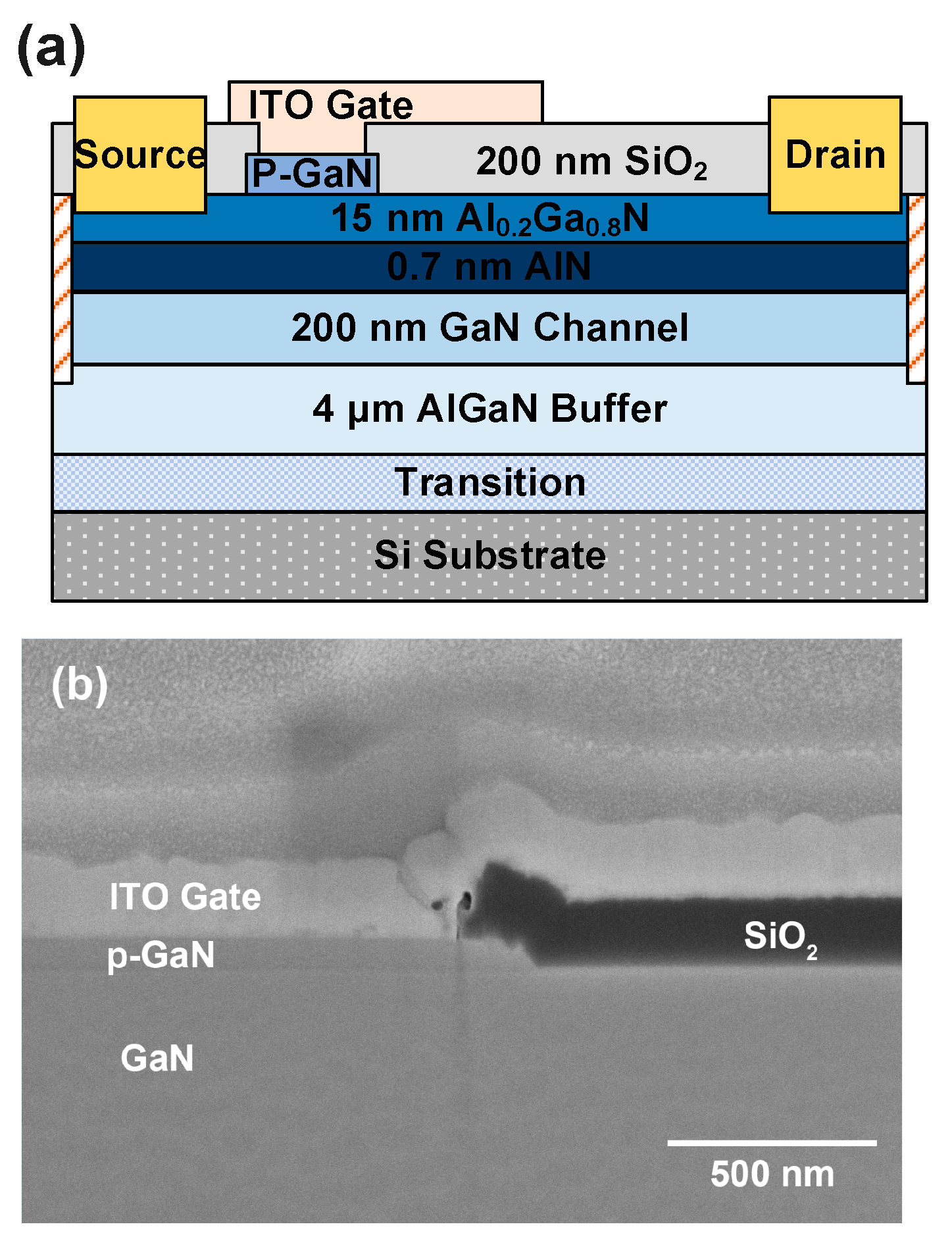
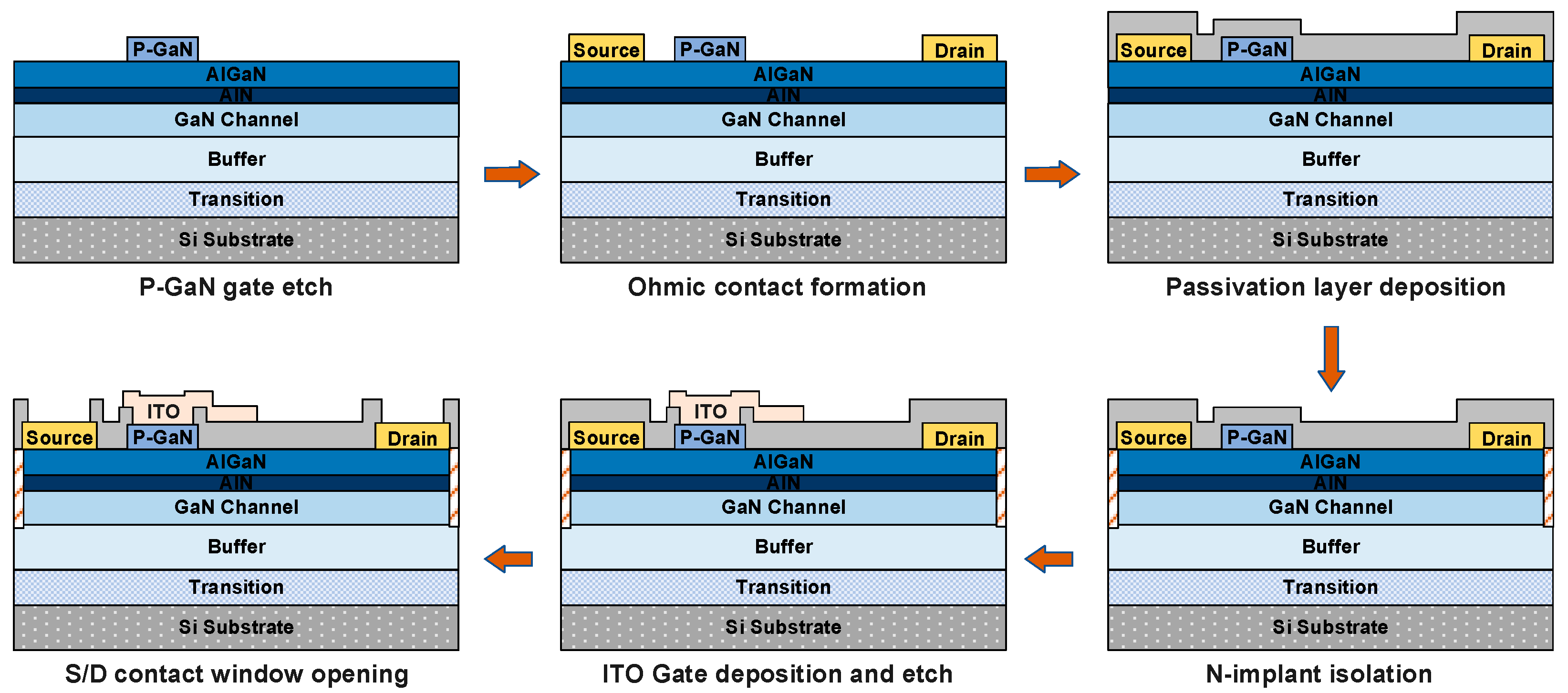
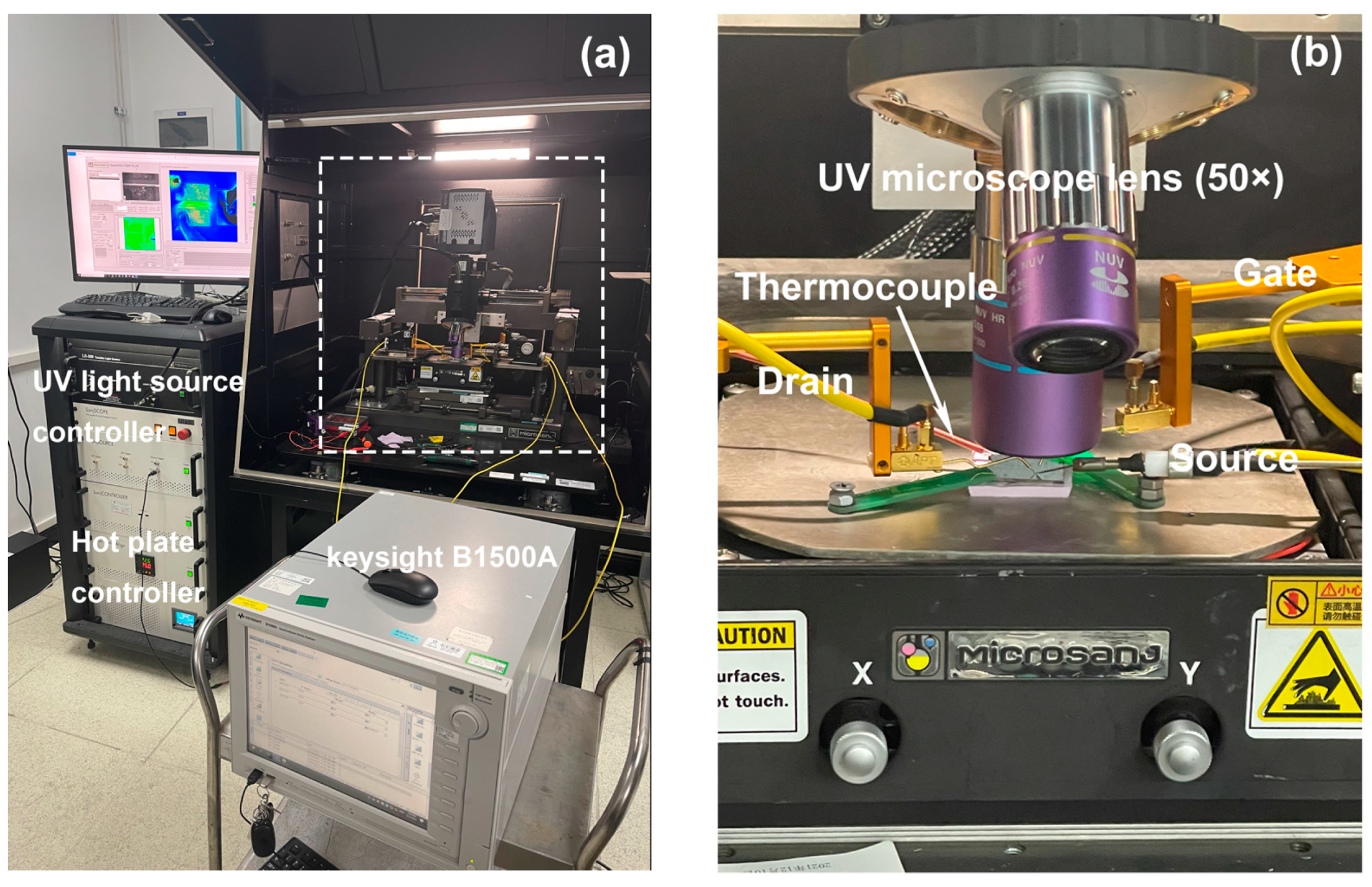
2. Materials and Methods
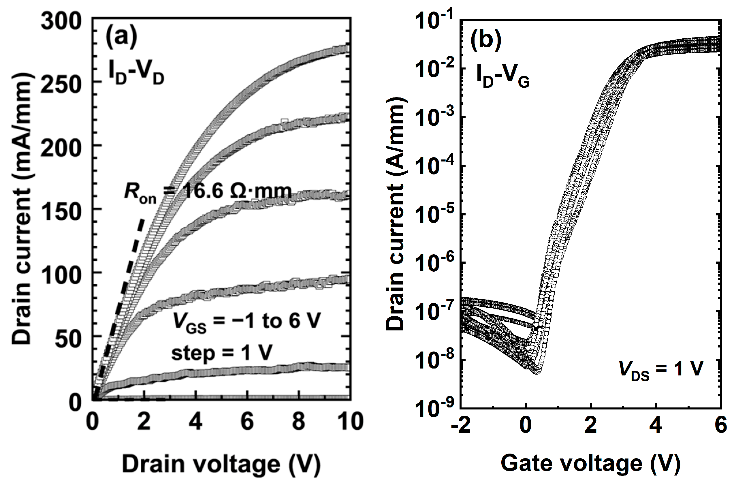
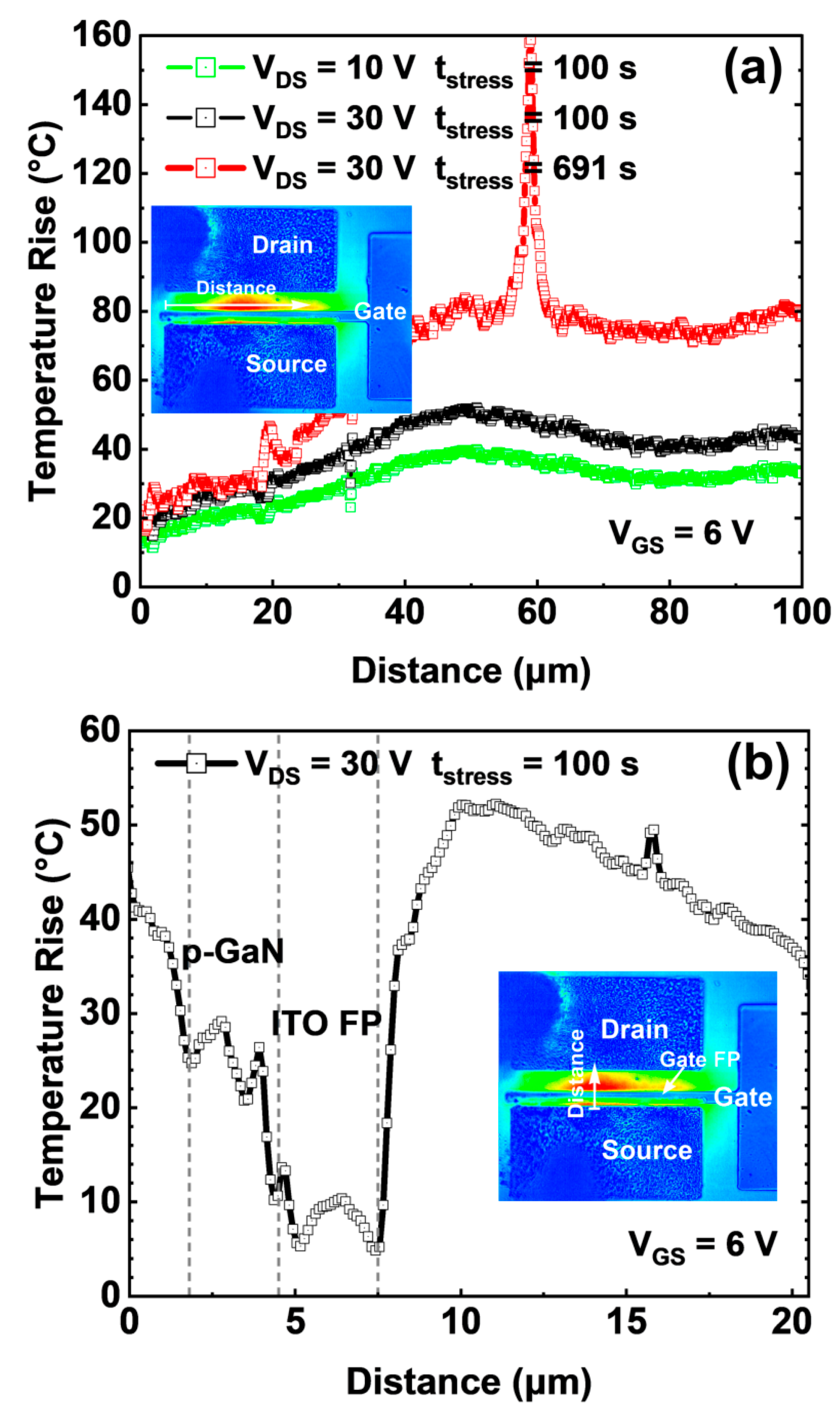
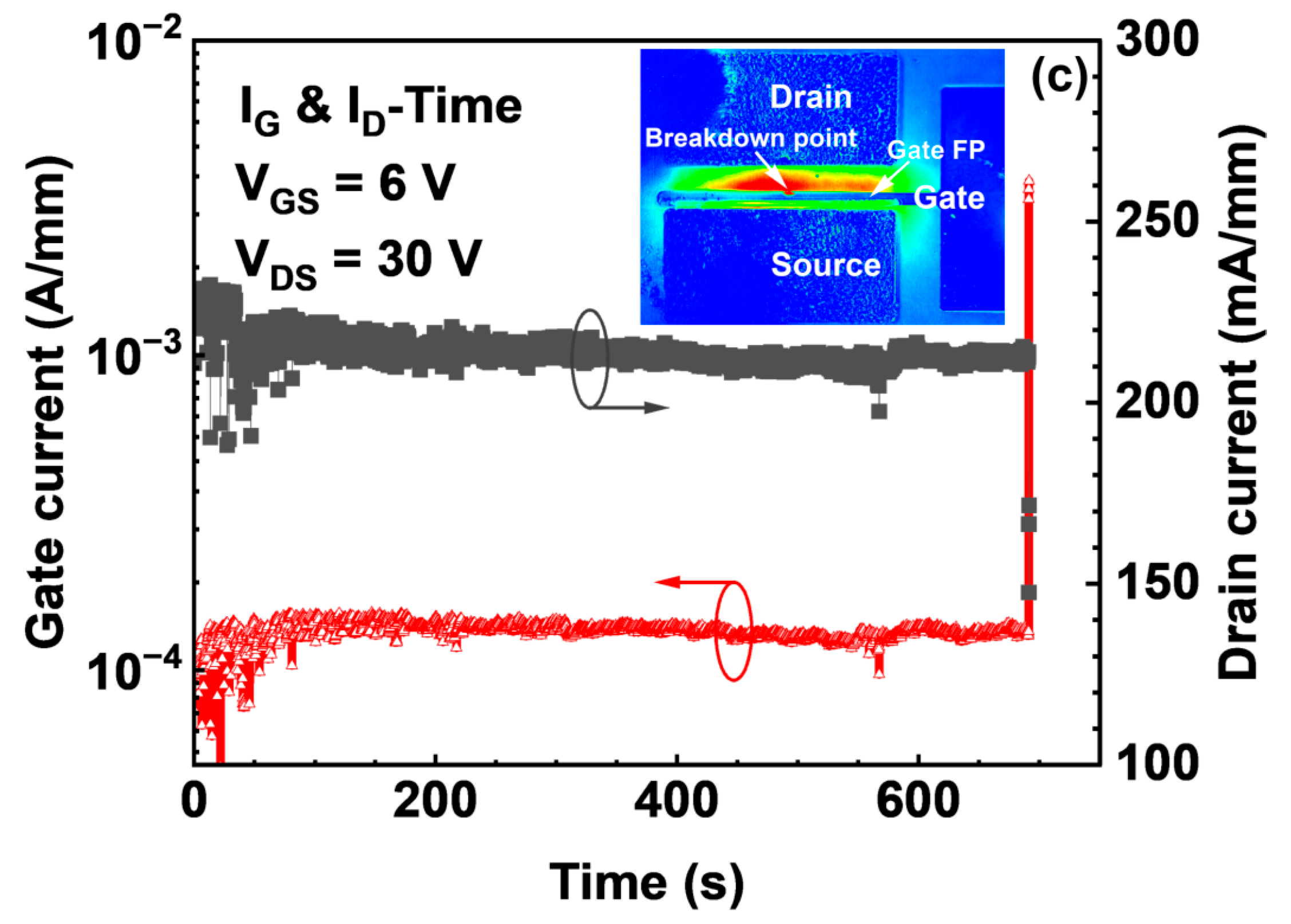
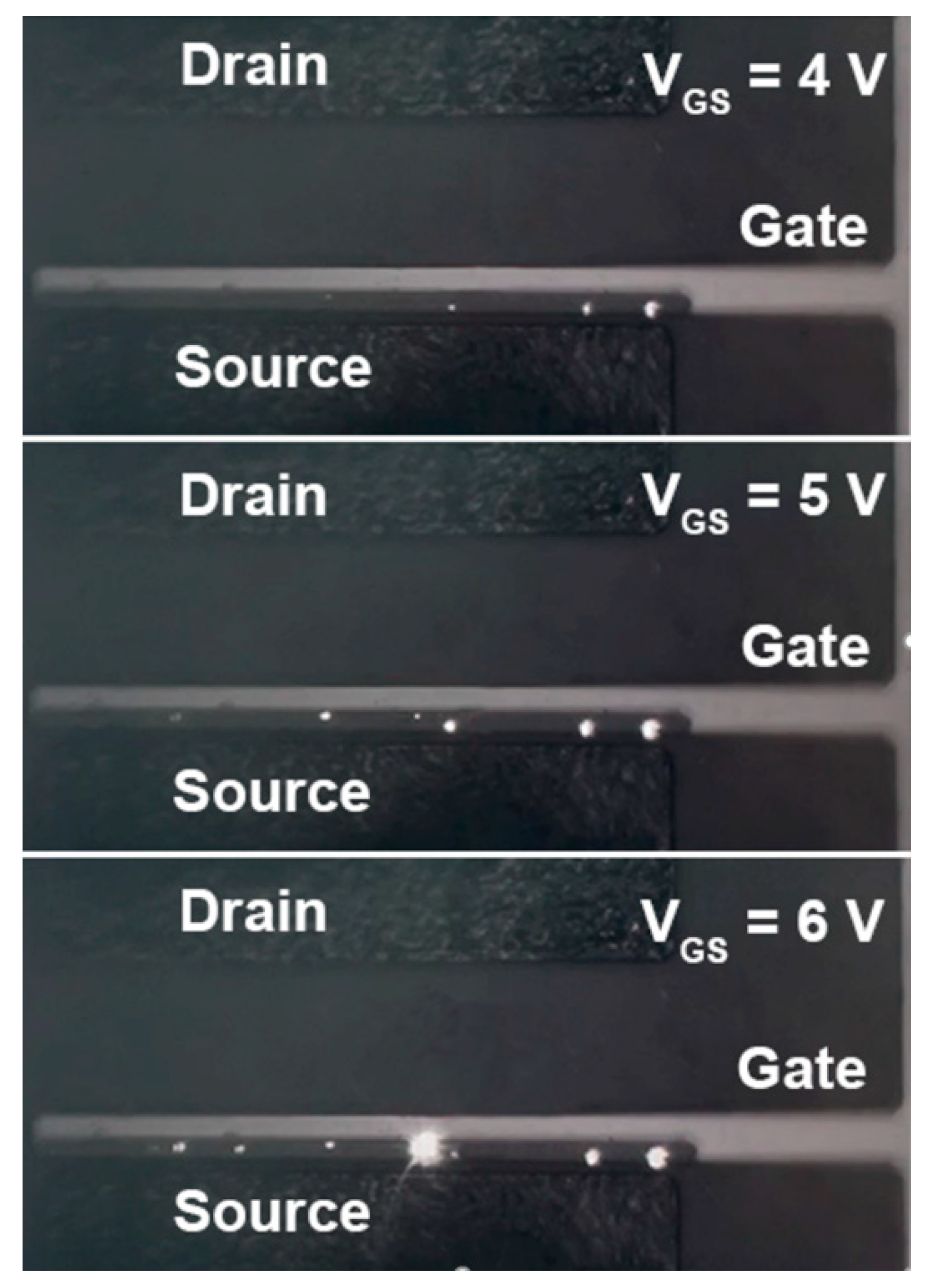
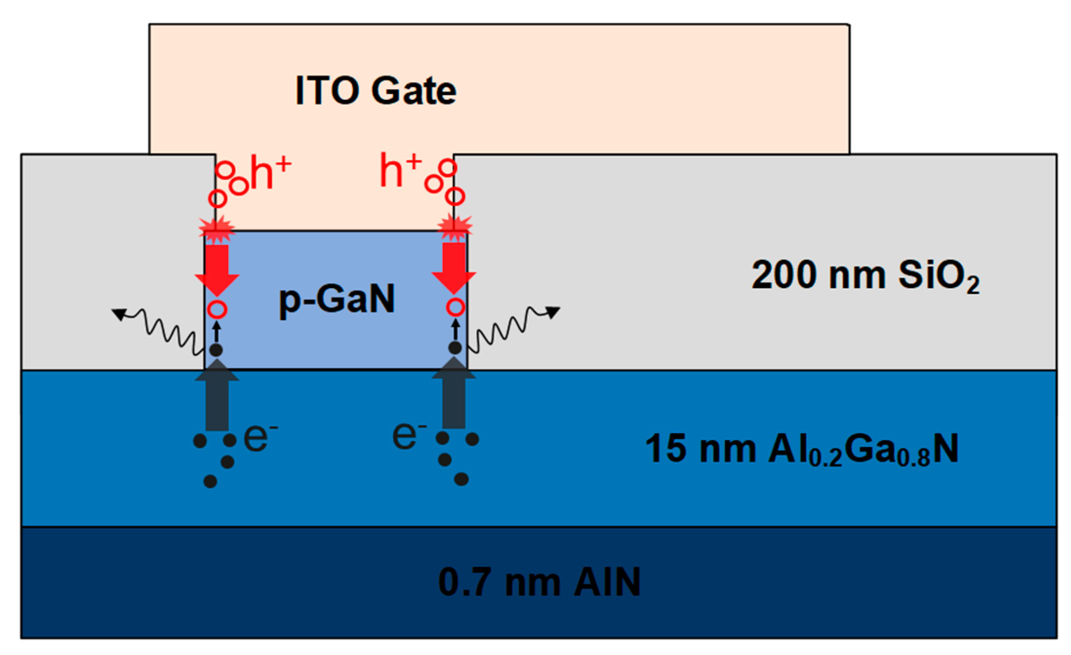
A p-GaN/AlGaN/GaN heterostructure was grown on a 6-inch Si <111> substrate via metal-organic chemical vapor deposition (MOCVD). The structure comprises a 4-µm thick AlGaN buffer layer, an unintentionally-doped 200-nm GaN channel layer, a 0.7-nm AlN layer, a 15-nm Al0.2Ga0.8N barrier layer, and a 70-nm p-GaN layer doped with a Mg doping concentration of 3 × 1019 cm−3. The electron mobility extracted using Hall measurement at room temperature was 1495 cm2/V·s.
The cross-sectional diagram of the ITO-gated p-GaN gate HEMTs is shown in Figure 1a, where an FIB-SEM photograph of the gate stack as well as the gate field plate is shown in Figure 1b. The device process flow is shown in Figure 2. This process highlights p-GaN selective etching by using Cl2/Ar/O2-based inductively coupled plasma (ICP), with the AlGaN barrier layer employed as a self-stopping layer. The surface roughness of the etched area was measured to be 0.35 nm via atomic force microscope (AFM) scanning. The device’s source and drain electrodes, Ti/Al/Ni/Au (22/140/50/40 nm), were deposited via electron beam evaporation, and ohmic contacts were achieved by rapid annealing at 865 °C for 30 s in the ambient of N2. The device’s passivation layer is a 200 nm SiO2 deposited by plasma-enhanced chemical vapor deposition (PECVD). The active region of the device was defined through multiple conditions of N ion implantation isolation to achieve an implantation depth of 300 nm. Finally, the gate region opening was patterned by lithography and then SiO2 etching. Afterwards, the ITO was deposited via evaporation as the gate material and patterned by IBE etching. During the ITO deposition, the substrate temperature was maintained at 350 °C. The fabricated devices have a gate length LG of 3 µm, a gate width WG of 100 µm, a gate-to-source distance LGS of 1.5 µm, and a gate-to-drain distance LGD of 16 µm.

3. Results

Figure 3a displays the typical ID-VD characteristics of the ITO-gated device. At VDS = 10 V and VGS = 6 V, the device exhibits a saturation drain current of 276 mA/mm and an on-state resistance of 16.6 Ω·mm. Figure 3b shows the ID-VG characteristics of the device, on which we can see the threshold voltage (VTH) is approximately 1.6 V under the criterion of ID = 0.1 mA/mm. The prepared device has a gate breakdown performance similar to that of a traditional Schottky gate.
In order to monitor the temperature distribution of the device under high power stress, thermal reflectivity imaging was used [28] and the test system setup is shown in Figure 4a. In this work, a 365 nm ultraviolet light-emitting diode light source and a 50× lens were equipped in the measurement system. Before the measurement, the reflectance is calibrated with a thermocouple that needs to be pressed against the sample surface for high accuracy, as shown in Figure 4b. Since the absorption wavelength of GaN material is 362 nm, the 365 nm light source that induces the photovoltaic effect will change the real voltage applied on the ITO gate. To suppress this impact, the frame rate is set to the minimum value of one when the reflectance is sampled.
Figure 5a illustrates the temperature distribution of the ITO-gated HEMTs along the horizontal cutline as depicted on the inset figure, where the VGS = 6 V and VDS = 10/20/30 V. We can unambiguously see that the heat is mainly concentrated in the center of the access area between the gate and drain terminal, which is induced by the electric field peak in the vicinity of the gate field plate edge, consistent with the conclusion reported in [29]. Figure 5b shows the temperature distribution of the ITO-gated HEMT along the vertical cutline from the source terminal’s upper edge to the drain terminal’s bottom edge. It is worthwhile noting that the temperature increase is not significant in the channel area under the gate field plate, thanks to the electric field modulation by the gate field plate. After a 691 s continuous power stress at VGS = 6 V and VDS = 30 V, a failure took place and the gate current saw a sudden jump, as shown in Figure 5c. We can clearly see a hot spot in the inset figure, corresponding to the breakdown point. The cause is probably that, during the p-GaN patterning, the ICP etching introduced enormous defect states on the sidewall of the p-GaN. In addition, the crowding effect of the electric field could accelerate the wear-out process on the sidewall and finally trigger the failure.
To further probe the failure mechanism of the device stressed by the high power shown in Figure 5, gate luminescence was monitored. Figure 6 illustrates that when VDS = 0 V and VGS vary at different voltages, luminescence can be observed from the failed p-GaN gate, thanks to the transparent ITO. It means the p-GaN gate stack works as a light-emitting diode (LED) after the gate failure. Normally, luminescence can be hardly observed because the hole injection from the gate metal to the p-GaN is difficult. However, in our case, the junction between the gate and p-GaN, as well as the p-GaN sidewalls, is quite vulnerable to the high power stress. The most obvious luminescence spot is located on the p-GaN sidewall in the central vicinity of the hottest area in Figure 6. It proves that the gate failure is accelerated by the heat generated by the high power stress. After gate failure, as shown in Figure 7, the Schottky barrier of the gate metal/p-GaN junction is destroyed, and the hole potential barrier is thus lowered, which strongly boosts the hole injection from the gate metal to the p-GaN layer. The abundant injected holes recombine with the electrons from the channel and thus photons are generated and observed.

4. Conclusions

In summary, by applying transparent ITO as the gate terminal onto the p-GaN gate HEMTs, the temperature distribution and luminescence of the devices under high power stress were successfully and unambiguously observed by ultraviolet light reflectivity testing. It was clearly concluded that the heat concentrated in the vicinity of the gate field plate in the access area, under the stress of VGS = 6 V and VDS = 10/20/30 V. After a 691 s high power stress, the device failed and the breakdown point was found to be located on the p-GaN. After failure, gate luminescence was found to be distributed on the sidewall of the p-GaN while positively biasing the gate, proving that the sidewall is the weakest spot of the p-GaN gate HEMTs under high power stress. Further optimization of the device processing is suggested to repair the processing damages on the sidewall. These findings above illustrate that the transparent ITO gate is a powerful tool for the reliability characterization of the p-GaN gate HEMTs. This tool can be also be applied in more complicated dynamic reliability tests in the future, considering the ns-level temporal accuracy of the ultraviolet light reflectivity testing system.

Author Contributions

Device design, Z.H., X.L., J.W., S.Y. and W.Y.; fabrication, Z.H. and J.W., characterization, Z.H., H.W., J.Y., X.L., M.W., J.W., S.Y. and W.Y., writing original draft preparation, Z.H., H.W., X.L., M.W., J.W., S.Y., J.C., J.Z. and Y.H. All authors have read and agreed to the published version of the manuscript.

Funding

This research was funded by the National Key Research and Development Program of China, grant number 2021YFB3600900, National Key Research and Development Program of China, grant number 2021YFA0715600, and National Natural Science Foundation of China, grant number 52192610.

Data Availability Statement

The data that support the findings of this study are available from the corresponding authors upon reasonable request.

Acknowledgments

The authors thank all members of the GaN Power Electronics Research Group, especially Xiangdong Li, Shuzhen You and Weitao Yang from the Guangzhou Institute of Technology, Xidian University, and Hongyue Wang from China Electronic Product Reliability and Environmental Testing Research Institute for making this study possible. At the same time, we would like to thank the processing platform provided by the Suzhou Institute of Nanotechnology and Nanobionics of the Chinese Academy of Sciences, and the test platform provided by the China Saibao Laboratory.

Conflicts of Interest

The authors declare no conflict of interest.

References

  1. Chen, K.-J.; Yang, F.; Lu, D.; Huang, H.; Shih, H.-Y.; Lee, P.-C.; Wu, Y.-H.; Wu, C.-Y.; Chang, H.-Y.; Lee, C.-H. kV-class GaN-on-Si HEMTs enabling 99% efficiency converter at 800 V and 100 kHz. IEEE Electron. Device Lett. 2014, 35, 1056–1058. [Google Scholar] [CrossRef]
  2. DasGupta, S.; Chowdhury, S.; Rajagopal, P. The 2018 GaN power electronics roadmap. IEEE J. Emerg. Sel. Top. Power Electron. 2018, 6, 58–78. [Google Scholar] [CrossRef]
  3. GaN Systems. GS66502B Datasheet. 2018. Available online: https://gansystems.com/datasheets/GS66502B-DS-Rev1.pdf (accessed on 1 March 2023).
  4. Efficient Power Conversion. EPC2019 Datasheet. 2019. Available online: http://epc-co.com/epc/documents/datasheets/EPC2019_datasheet.pdf (accessed on 1 March 2023).
  5. Mandal, S.; DasGupta, S.; Pratap, R.; Rajagopal, P. Observation of dynamic VTH of p-GaN gate HEMTs by fast sweeping characterization. IEEE Trans. Electron Device 2012, 59, 2820–2827. [Google Scholar] [CrossRef]
  6. Lee, W.; Hsu, J.; Wu, C.; Lai, E.; Cheng, H. Gate architecture design for enhancement mode p-GaN gate HEMTs for 200 and 650 V applications. IEEE Trans. Electron Devices 2014, 61, 1489–1494. [Google Scholar] [CrossRef]
  7. Huang, Y.-C.; Chen, G.-R.; Chen, K.-M. 200 V enhancement-mode p-GaN HEMTs fabricated on 200 mm GaN-on-SOI with trench isolation for monolithic integration. IEEE J. Electron Devices Soc. 2017, 5, 10–16. [Google Scholar] [CrossRef]
  8. Chang, P.-H.; Huang, J.; Tsai, J. Wide energy bandgap electronic devices. J. Electron. Sci. Technol. China 2017, 15, 219–229. [Google Scholar] [CrossRef]
  9. Meneghesso, G.; Sabui, G.; Zanoni, E. Challenges for energy efficient wide band gap semiconductor power devices. IEEE Trans. Electron Devices 2017, 64, 3655–3667. [Google Scholar] [CrossRef]
  10. Wei, Y.-T.; Chou, H.-C.; Wu, Y.-H.; Yang, F.; Lee, C.-H. Demonstration of Schottky barrier diode integrated in 200 V power p-GaN HEMTs technology with robust stability. IEEE J. Electron Devices Soc. 2016, 4, 37–41. [Google Scholar] [CrossRef]
  11. Chow, T.-P.; Morkoç, H. GaN-on-Si power technology: Devices and applications. IEEE Trans. Electron Devices 2010, 57, 2245–2254. [Google Scholar] [CrossRef]
  12. Wang, J.; Li, P.; Yuan, Y.; Zhang, J.; Tian, Q.; Liu, Y.; Chen, J.; Li, X.; Zhao, T. Normally-off high-voltage p-GaN gate GaN HFET with carbon-doped buffer. IEEE Electron Device Lett. 2017, 38, 748–751. [Google Scholar] [CrossRef]
  13. Sasaki, T.; Otsuka, T.; Tsukahara, Y.; Nakano, Y. Enhancement-mode GaN-based high-electron mobility transistors on the Si substrate with a P-type GaN cap layer. IEEE Trans. Electron Devices 2015, 62, 3145–3150. [Google Scholar] [CrossRef]
  14. Xu, W.; Chen, D.; Wu, D.; Zhang, J.; Yang, Z.; Shen, B.; Zhang, J. Effects of annealing treatments on the properties of Al/Ti/p-GaN interfaces for normally off p-GaN HEMTs. Appl. Surf. Sci. 2017, 409, 66–71. [Google Scholar] [CrossRef]
  15. Wang, T.; Jiang, L.; Zhang, M.; Jiang, Y. A novel physics-based approach to analyze and model E-mode p-GaN power HEMTs. IEEE Trans. Power Electron. 2019, 34, 1524–1534. [Google Scholar] [CrossRef]
  16. Kim, J.; Lee, K.; Hwang, J.; Lee, M.; Lee, J.; Lee, S.; Kang, S.; Lee, J.; Nam, O.; Lee, H.; et al. High-voltage and low-leakage-current gate recessed normally-off GaN MIS-HEMTs with dual gate insulator employing PEALD-SiNx/RF-sputtered-HfO2. IEEE Trans. Electron Devices 2016, 63, 3476–3479. [Google Scholar] [CrossRef]
  17. Zhang, J.; Jang, J.; Kim, H.; Lee, J. Monolithic integration of lateral field-effect rectifier with normally-off HEMT for GaN-on-Si switch-mode power supply converters. IEEE Trans. Power Electron. 2015, 30, 2518–2523. [Google Scholar] [CrossRef]
  18. Chowdhury, S.; Mishra, U.; Deshpande, D. An overview of normally-off GaN-based high electron mobility transistors. Proc. IEEE 2012, 100, 2857–2871. [Google Scholar] [CrossRef]
  19. Xu, C.; Xu, Q.; Wang, M.; Liu, Y.; Zhang, Y.; Li, M.; Li, Y. Time-dependent failure of GaN-on-Si power HEMTs with p-GaN gate. IEEE Trans. Device Mater. Reliab. 2019, 19, 302–307. [Google Scholar] [CrossRef]
  20. Kim, C.; Cho, H.; Cho, N.; Lee, J. Gate current transport in enhancement-mode p-nJunction/AlGaN/GaN (PNJ) HEMT. J. Korean Phys. Soc. 2017, 71, 273–277. [Google Scholar] [CrossRef]
  21. Kim, M.; Oh, S.; Kim, S.; Kim, S.; Ju, S.; Hong, Y. Improved gate reliability normally-off p-GaN/AlN/AlGaN/GaN HEMT with AlGaN cap-layer. IEEE Electron Device Lett. 2017, 38, 1055–1058. [Google Scholar] [CrossRef]
  22. Krishnaswamy, N.; Sohal, M.; Palmour, J.W. Forward Bias Gate Breakdown Mechanism in Enhancement-Mode p-GaN Gate AlGaN/GaN High-Electron Mobility Transistors. IEEE Trans. Electron Devices 2018, 65, 3429–3434. [Google Scholar]
  23. Takeishi, T.; Muraguchi, M.; Katayama, R.; Tanaka, T. Gate injection transistor (GIT)—A normally-off AlGaN/GaN power transistor using conductivity modulation. Proc. IEEE Trans. Electron Devices 2008, 55, 1806–1813. [Google Scholar]
  24. Johnson, C.M. Reliability Issues in GaN and SiC Power Devices. In Proceedings of the IEEE Transactions on Device and Materials Reliability, Waikoloa, HI, USA, 1–5 June 2013; Volume 13, pp. 394–406. [Google Scholar]
  25. Kim, S.; Kim, S.; Kim, T.; Kim, G.; Kwon, H.-I.; Kwon, Y. Demonstration of p-GaN/AlGaN/GaN high electron mobility transistors with an indium-tin-oxide gate electrode. Appl. Phys. Lett. 2017, 110, 183503. [Google Scholar] [CrossRef] [Green Version]
  26. Yang, X.; Li, J.; Li, X.; Li, H.; Liang, S.; Du, S.; Zhou, S. Investigation on stability of p-GaN HEMTs with an indium-tin-oxide gate under forward gate bias. Microelectron. Reliab. 2019, 97, 155–159. [Google Scholar] [CrossRef]
  27. Wu, Y.; Chen, Q.; Zhang, C.; Yang, B.; Xu, J.; Zhang, Y.; Chen, Z.; Lu, J. Fully transparent AlGaN/GaN high electron mobility transistors fabricated with indium-tin-oxide electrodes. Appl. Phys. Lett. 2019, 114, 052103. [Google Scholar] [CrossRef]
  28. Verzellesi, G.; Meneghesso, G.; Zanoni, E.; Rampazzo, F.; Paccagnella, A.; Van Hove, M. Transient thermal characterization of AlGaN/GaN HEMTs under pulsed biasing. IEEE Trans. Electron Devices 2013, 60, 1705–1712. [Google Scholar] [CrossRef]
  29. Oh, H.; Kim, D.; Choi, M.; Kim, B.; Lee, H. Charge storage impact on input capacitance in p-GaN gate AlGaN/GaN power high-electron-mobility transistors. Jpn. J. Appl. Phys. 2014, 53, 04EC08. [Google Scholar] [CrossRef] [Green Version]
Figure 1. (a) Cross-sectional diagram of a p-GaN gate HEMTs with an ITO gate. (b) FIB-SEM photograph of the device’s gate stack as well as the gate field plate above the SiO2 passivation layer.
Micromachines 14 00940 g001
Figure 2. Simplified fabrication process of the ITO-gated p-GaN gate HEMTs.
Micromachines 14 00940 g002
Figure 3. (a) Output and (b) transfer characteristics of the ITO-gated p-GaN gate HEMTs at room temperature.
Micromachines 14 00940 g003
Figure 4. (a) The thermal reflectivity imaging system, including electrical measurement, heat measurement, and reflectance calibration section. (b) The details of the system dotted box in (a).
Micromachines 14 00940 g004
Figure 5. (a) The temperature distribution of the ITO-gated HEMTs along the horizontal cutline as depicted on the inset figure, under the stress of VGS = 6 V and VDS = 10/20/30 V. (b) The temperature distribution of the ITO-gated HEMTs from the source terminal’s upper edge to the drain terminal’s bottom edge, under the stress of VGS = 6 V and VDS = 30 V by tstress = 100 s. (c) The temperature distribution of the ITO-gated HEMTs under the stress of VGS = 6 Vand VDS = 30 V by tstress = 691 s until the failure took place.
Micromachines 14 00940 g005aMicromachines 14 00940 g005b
Figure 6. Photos of ITO-gated p-GaN gate HEMTs luminescence under VDS = 0 V and various VGS after gate failure.
Micromachines 14 00940 g006
Figure 7. Gate failure and luminescence mechanism of the p-GaN gate HEMTs.
Micromachines 14 00940 g007
Disclaimer/Publisher’s Note: The statements, opinions and data contained in all publications are solely those of the individual author(s) and contributor(s) and not of MDPI and/or the editor(s). MDPI and/or the editor(s) disclaim responsibility for any injury to people or property resulting from any ideas, methods, instructions or products referred to in the content.

