Abstract
In recent years, the active-matrix organic light-emitting diode (AMOLED) displays have been greatly required. A voltage compensation pixel circuit based on an amorphous indium gallium zinc oxide thin-film transistor is presented for AMOLED displays. The circuit is composed of five transistors–two capacitors (5T2C) in combination with an OLED. In the circuit, the threshold voltages of both the transistor and the OLED are extracted simultaneously in the threshold voltage extraction stage, and the mobility-related discharge voltage is generated in the data input stage. The circuit not only can compensate the electrical characteristics variation, i.e., the threshold voltage variation and mobility variation, but also can compensate the OLED degradation. Furthermore, the circuit can prevent the OLED flicker, and can achieve the wide data voltage range. The circuit simulation results show that the OLED current error rates (CERs) are lower than 3.89% when the transistor’s threshold voltage variation is ±0.5V, lower than 3.49% when the mobility variation is ±30%.
1. Introduction
OLEDs (organic light-emitting diodes) have gained widespread attention for their advantages such as low power consumption, high contrast, fast response time, thinner, and more foldable characteristics. According to the different driving methods, OLED driving technology can be divided into PMOLEDs (passive-matrix OLEDs) and AMOLED (active-matrix OLEDs). PMOLED has the advantages of a simple structure and low cost. However, PMOLED requires a larger driving voltage, and its power consumption is significantly higher than the AMOLED. As shown in Figure 1, AMOLEDs use independent thin-film transistors to control each pixel, so that each pixel can be continuously and independently driven and lit. Therefore, AMOLED is suitable for large and high-resolution displays, and has high application prospects for the displays [1,2,3,4].
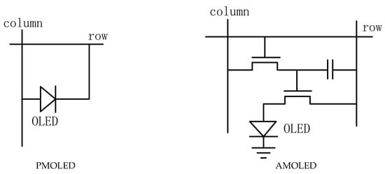
Figure 1.
Schematic of PMOLED and AMOLED [4].
In AMOLED pixel circuits, the oxide thin-film transistor (TFT) has great advantages, such as high carrier mobility, high light transmittance, good uniformity, and low off current, so it is widely applied to drive OLED, especially for large size AMOLED [5,6,7,8,9].
On the one hand, the TFT’s electrical characteristics variation, i.e., the threshold voltage variation and mobility variation would lead to the OLED current change. On the other hand, the OLED degradation would also lead to the OLED current change. The OLED current change brings out the uniformity of displays [10,11]. Therefore, in AMOLED displays, the circuit is needed to compensate the TFT’s electrical characteristics’ variation and the OLED degradation. Generally, the compensation circuit is divided into the current compensation circuit and the voltage compensation circuit.
The current compensation circuit can successfully compensate the TFT’s electrical characteristics’ variation [12,13]. However, the compensation speed is relatively slow at low gray level. This problem could be solved by the voltage compensation circuit [14,15,16].
Therefore, lots of valuable voltage compensation pixel circuits have been reported [17,18,19,20,21,22,23,24,25,26,27,28,29,30].
In [17,18,19,20,21], the circuits can compensate the threshold voltage variation successfully. In [22,23,24,25], the circuits can compensate both threshold voltage and mobility variations successfully. In [26,27,28], the circuits can compensate both threshold voltage variation and OLED degradation successfully. To obtain higher uniformity of displays, it would be better if the circuits can compensate the above three items.
In [29], the circuit can compensate the above three items successfully, but the circuit cannot prevent the OLED flicker. In [30], the circuit not only can compensate the above three items, but also can prevent the OLED flicker successfully. However, the data voltage must be less than the OLED threshold voltage. Thus, the data voltage range is limited.
In this paper, a voltage compensation pixel circuit is proposed. In the threshold voltage extraction stage, the circuit can extract the threshold voltages of both the TFT and the OLED simultaneously. In the data input stage, the circuit can generate the mobility-related discharge voltage. The simulation results show that the circuit can compensate three items: the threshold voltage variation, the mobility variation, and the OLED degradation, can prevent the image flicker, and can achieve the wide data voltage range.
2. Materials and Methods
The circuit structure and the driving schematic diagram are shown in Figure 2. As shown in Figure 2a, the circuit consists of one driving TFT (T2), four switching TFTs (T1, T3, T4, T5), and two capacitors (C1, C2).
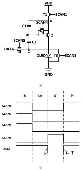
Figure 2.
(a) Schematic of the proposed pixel circuit and (b) timing diagram: (1) initialization stage, (2) threshold voltage extraction stage, (3) data input stage, and (4) emission stage.
As shown in Figure 2b, the driving schematic diagram contains four stages: (1) the initialization stage, (2) the threshold voltage extraction stage, (3) the data input stage, and (4) the emission stage.
The working principle of the circuit is described as follows.
2.1. Initialization Stage
In the initialization stage, as shown in Figure 2b, SCAN1, SCAN3, and SCAN4 are high. SCAN5 is low. Therefore, T1, T3, and T4 are turned on. T5 is turned off. The schematic of the circuit in this stage is shown in Figure 3a.
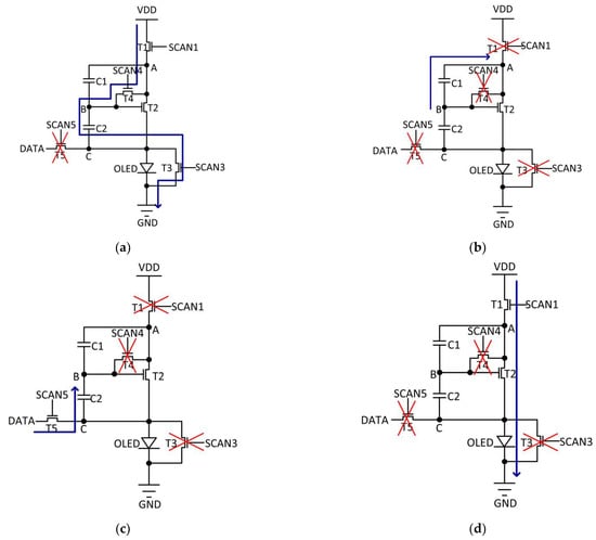
Figure 3.
Schematic of the circuit operation in (a) initialization stage, (b) threshold voltage extraction stage, (c) data input stage, and (d) emission stage.
Because T1 and T4 are turned on, the voltage of node B is charged to VDD.
Because T3 is turned on, no current flows through the OLED. Therefore, the OLED flicker is prevented.
2.2. Threshold Voltage Extraction Stage
In the threshold voltage extraction stage, as shown in Figure 2b, SCAN1, SCAN3, and SCAN4 go to low. SCAN5 remains low. Therefore, T1, T3, T4, and T5 are turned off. The schematic of the circuit in this stage is shown in Figure 3b.
Because T1 is turned off, no current flows through the OLED. Therefore, the OLED flicker is prevented.
The voltage of node B is gradually discharged until T2 is turned off. The voltage of node B goes to
Consequently, the threshold voltages of both T2 and OLED are extracted simultaneously in this stage.
2.3. Data Input Stage
In the data input stage, as shown in Figure 2b, SCAN1, SCAN3 and SCAN4 remain low; SCAN5 goes to high. Therefore, T1, T3, and T4 are turned off; T5 is turned on. The schematic of the circuit in this stage is shown in Figure 3c.
Because T1 is turned off, no current flows through the OLED. Therefore, the OLED flicker is prevented.
In [29], to prevent OLED flicker, the data voltage range is limited: it is much less than the OLED threshold voltage. In this paper, the above limitation is avoided.
At the beginning and the end of this stage, t is defined as t0 and t0 + T, respectively. They are indicated in Figure 2b.
At the time t0, the data voltage (VDATA) is input to the circuit; VC and VB are expressed as
After the time T, VC remains unchanged; VB discharges through C1, C2, and T2. At the time t0 + T, VC and VB are expressed as
where is the discharged voltage related to the mobility of T2.
The expression of is derived as follows. When DATA is input to the circuit, T2 keeps the diode-connected structure. Therefore, the mobility-related discharge voltage is stored in C1. By the law of discharge conservation, we have [30]
where is the mobility of T2, COX is the gate oxide capacitance per unit area, and is the width–length ratio of T2.
Integrating (6), we have
where
Substituting (2)–(5) to (9), we obtain
Consequently, the mobility-related discharge voltage is generated in this stage.
2.4. Emission Stage
In the emission stage, as shown in Figure 2b, SCAN1 goes to high, SCAN3 and SCAN4 remain low, and SCAN5 goes to low. Therefore, T1 is turned on, and T3, T4, and T5 are turned off.
The schematic of the circuit in this stage is shown in Figure 3d.
The driving TFT (T2) operates in the saturation region; the OLED current is expressed as follows:
Substituting (9) to (11), we obtain
Substituting (10) to (12), we obtain
From (12), it is found that the OLED current is independent of the threshold voltage VTH_T2. That is, when VTH_T2 varies, IOLED remains stable. Therefore, the circuit can compensate the threshold voltage variation.
From (10), it is found that when the mobility increases, will increase, and vice versa. Consequently, in (12), when the mobility varies, IOLED remains stable. Therefore, the circuit can compensate the mobility variation. This point also can be explained by (13). In (13), when increases, both and will increase; thus, IOLED remains stable, and vice versa.
From (13), it is found that the OLED current is positively correlated with VTH_OLED. Therefore, the circuit can compensate the OLED degradation [29,30,31].
3. Results and Discussions
In the circuit simulation, to evaluate the compensation performance, the SPICE model (level = 35) is used for the oxide TFTs. The TFTs’ threshold voltage and mobility are 1.5 V and 50 cm2/V, respectively. The TFTs’ threshold voltage variation and mobility variation are ±0.5 V and ±30%, respectively [9,14,28]. The OLED model is equivalent to a TFT and a COLED in parallel [22,27,32]. The oxide TFT and the OLED models are verified by the experimental data [8,33], which are shown in Figure 4.
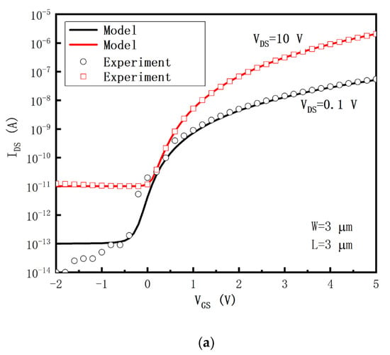
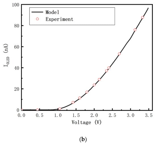
Figure 4.
(a) The transfer characteristic of the a-IGZO TFT [8], and (b) the electrical characteristic of the OLED [33].
The values of the design parameters are shown in Table 1; the range of the values is reasonable, which is consistent with the previous pixel circuit applications [11,19,20,27,32,34].

Table 1.
Design parameters of the circuit.
Figure 5a shows the transient waveforms of VB, i.e., the gate voltage of T2, at VDATA = −4 V. It is found that when ΔVTH_T2 = ±0.5 V, ΔVB approximates ±0.5 V in the threshold voltage extraction stage, i.e., VB senses the threshold voltage variation successfully. Figure 5b shows the transient waveforms of the OLED current IOLED. It is found that IOLED = 0 except for the emission stage, i.e., the OLED flicker is prevented. In the emission stage, when ΔVTH_T2 = −0.5, 0, and +0.5 V, the transient waveforms of IOLED = 94.11, 90.59, and 87.06 n A, respectively. The current error rates (CERs) are 3.74% and 0, 3.89%, respectively. Thus, the circuit compensates ΔVTH_T2 successfully.
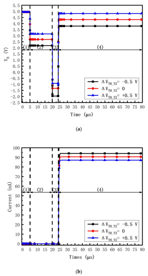
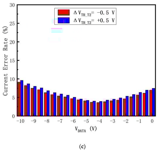
Figure 5.
Transient waveforms of (a) VB and (b) IOLED when ΔVTH_T2 = −0.5, 0, and +0.5 V at VDATA = −4 V, where (1) initialization stage, (2) threshold voltage extraction stage, (3) data input stage, (4) emission stage, and (c) current error rates versus VDATA when the threshold voltage varies.
The CER for ΔVTH_T2 is defined as
Figure 5c shows the transient waveforms of CER vary when ΔVTH_T2 is +0.5 V and −0.5 V, respectively. It is found that the CERs are less than ±9.59% within the whole data range. Thus, the threshold voltage variation ΔVTH_T2 is compensated successfully.
Figure 6a shows the transient waveforms of VB at VDATA = −4V. It is found that when Δu= ±30%, the variation of VB is similar to Δu, i.e., VB senses the mobility variation successfully. Figure 6b shows the transient waveforms of the OLED current IOLED. It is found that IOLED = 0 except for the emission stage, i.e., the OLED flicker is prevented. In the emission stage, when Δu = −30, 0, and +30%, the transient waveforms of IOLED = 88.06, 90.59, and 93.87 n A, respectively. The current error rates are 2.81% and 0, 3.49%, respectively. Thus, the circuit compensates Δu successfully.
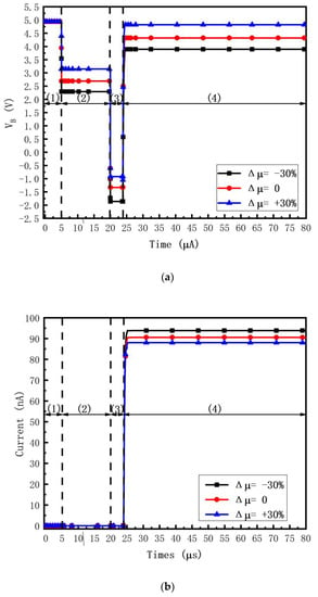
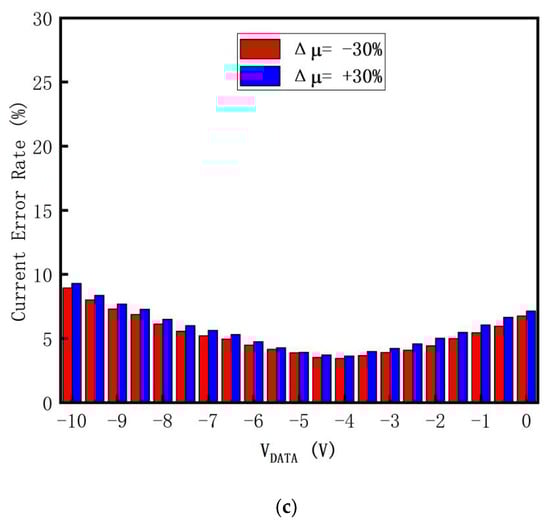
Figure 6.
Transient waveforms of (a) VB and (b) IOLED when Δu = +30%, 0, and −30% at VDATA= −4V, where (1) initialization stage, (2) threshold voltage extraction stage, (3) data input stage, (4) emission stage, and (c) current error rates versus VDATA when the threshold voltage varies.
The CER for Δu is defined as
Figure 6c shows the transient waveforms of CER varies when Δu is +30% and −30%, respectively. It is found that the CERs are less than ±9.28% within the whole data range. Thus, the mobility variation Δu is compensated successfully.
In this paper, the circuit can compensate the OLED degradation. It is explained as follows. For the long time operation, the OLED luminance degrades while VTH_OLED increases [29,30,31]. Therefore, IOLED (13) increases. The increase in IOLED brings about the increase in the OLED luminance. Thus, the OLED luminance degradation is compensated.
In Figure 5a,b and Figure 6a,b, the time of the third stage, i.e., the data input stage, is set to 3.8 us. It is suitable for the 8K4K ultrahigh definition (7680 × 4320, UHD) for high-performance display [11,35,36].
As shown in Table 2, the valuable publications are compared with this paper. In [29], the circuit can compensate the threshold voltage variation, the mobility variation, and the OLED degradation successfully, but the circuit cannot prevent the OLED flicker. In [30] and this paper, the circuits not only can compensate the above three items successfully, but also can prevent the OLED flicker.
Table 2.
Comparison between this paper and the previous publications.
However, in [30], VDATA must be less than VTH_OLED, that is, the range of VDATA is limited. In this paper, the range of VDATA is not limited by VTH_OLED. Therefore, the circuit achieves the wide data voltage range.
Figure 7 shows the layout structure of the circuit. SCAN1, SCAN3, SCAN4, and SCAN5 are transverse lines, which are set to 4 um. These transverse lines are shared by the pixels of the same row. VDD, GND, and DATA are the vertical lines, which are set to 6 um. VDD and GND are shared by the entire display panel. DATA is shared by the pixels of the same column. The total layout area is 180 um × 110 um. The proposed layout achieves an aperture ratio of 39.14%.
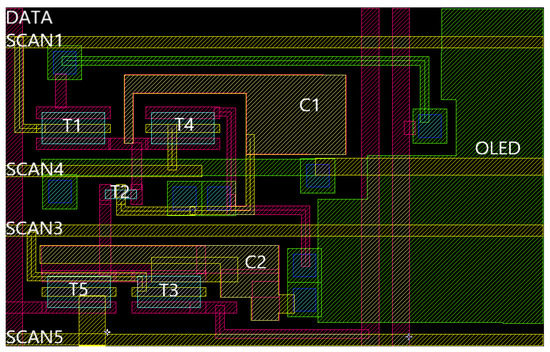
Figure 7.
Layout structure of the circuit.
4. Conclusions
The pixel circuit is presented for improving AMOLED displays uniformity. In the threshold voltage extraction stage, the threshold voltages of the driving TFT and the OLED are extracted. In the data input stage, the discharge voltage related to mobility is generated. Consequently, the circuit not only compensates the threshold voltage variation, the mobility variation, and the OLED degradation, but also prevents the image flicker and achieves the wide data voltage range.
Author Contributions
N.W.: Conceptualization, Methodology, Validation, Formal Analysis, Investigation, Writing—Original Draft; H.C.: Investigation; B.Y.: Investigation; H.Z.: Investigation; Y.L.: Supervision, Writing—Review & Editing; X.W.: Project Administration, Funding Acquisition; H.H.: Supervision, Writing—Review & Editing. All authors have read and agreed to the published version of the manuscript.
Funding
This research was funded by [The Hunan Province Key Laboratory for Ultra-Fast Micro/Nano Technology and Advanced Laser Manufacture] grant number [No. 2018TP1041].
Data Availability Statement
Data sharing is not applicable to this article as no new data were created or analyzed in this study.
Conflicts of Interest
The authors declare no conflict of interest.
References
- Singh, A.; Goswami, M.; Kandpal, K. Design of a voltage-programmed VTH compensating pixel circuit for AMOLED displays using diode-connected a-IGZO TFT. IET Circuits Devices Syst. 2020, 14, 876–880. [Google Scholar] [CrossRef]
- Srivastava, A.; Dubey, D.; Goswami, M.; Kandpal, K. Mechanical strain and bias-stress compensated, 6T-1C pixel circuit for flexible AMOLED displays. Microelectron. J. 2021, 117, 105266. [Google Scholar] [CrossRef]
- Zhao, B.; Xiao, J.; Liu, Q.; Liu, B.; Hu, L.; Peng, J. A novel compensation pixel circuit for high bits of AM mini/micro-LED based on PWM method. Energy Rep. 2021, 7, 343–348. [Google Scholar] [CrossRef]
- Lin, C.-L.; Chang, W.-Y.; Hung, C.-C.; Tu, C.-D. LTPS-TFT pixel circuit to compensate for OLED luminance degradation in three-dimensional AMOLED display. IEEE Electron Device Lett. 2012, 33, 700–702. [Google Scholar] [CrossRef]
- Lee, J.S.; Chang, S.; Koo, S.-M.; Lee, S.Y. High-performance a-IGZO TFT with ZrO2 gate dielectric fabricated at room temperature. IEEE Electron Device Lett. 2010, 31, 225–227. [Google Scholar] [CrossRef]
- Yao, J.; Xu, N.; Deng, S.; Chen, J.; She, J.; Liu, P.; Huang, Y. Electrical and photosensitive characteristics of a-IGZO TFTs related to oxygen vacancy. IEEE Trans. Electron Devices 2011, 58, 1121–1126. [Google Scholar] [CrossRef]
- Hong, S.-K.; Kim, B.-K.; Ha, Y.-M. LTPS technology for improving the uniformity of AMOLEDs. SID Symp. Dig. 2007, 38, 1366–1369. [Google Scholar] [CrossRef]
- Liao, C. Mobility impact on compensation performance of AMOLED pixel circuit using IGZO TFTs. J. Semicond. 2019, 40, 022403. [Google Scholar] [CrossRef]
- Lin, C.-L.; Chen, F.-H.; Liu, Y.-T.; Lu, C.-M.; Wu, W.-L. New voltage-programmed AMOLED pixel circuit employing in-pixel compensation scheme for mobility variation. SID Symp. Dig. 2016, 47, 1254–1256. [Google Scholar] [CrossRef]
- Lin, Y.-C.; Shieh, H.-P.D.; Kanicki, J. A novel current-scaling a-Si: H TFTs pixel electrode circuit for AM-OLEDs. IEEE Trans. Electron Devices 2005, 52, 1123–1131. [Google Scholar] [CrossRef]
- Lai, P.-C.; Lin, C.-L.; Kanicki, J. Novel top-anode OLED/a-IGZO TFTs pixel circuit for 8K4K AM-OLEDs. IEEE Trans. Electron Devices 2018, 66, 436–444. [Google Scholar] [CrossRef]
- Pappas, I.; Voudouris, L.; Tarawneh, B.K.; Rjoub, A.; Nikolaidis, S. A new current-programmed pixel design for AMOLED displays implemented with organic thin-film transistors. In Proceedings of the 2012 28th International Conference on Microelectronics Proceedings, Nis, Serbia, 13–16 May 2012; pp. 77–80. [Google Scholar] [CrossRef]
- Lee, J.-H.; Nam, W.-J.; Jung, S.-H.; Han, M.-K. A New Current Scaling Pixel Circuit for AMOLED. IEEE Electron Device Lett. 2004, 25, 280–282. [Google Scholar] [CrossRef]
- Zeng, Y.; Chu, H.; Wei, N.; Li, Y.; Wang, X.; He, H. A 5T1C pixel circuit compensating mobility and threshold voltage variation. Microelectron. J. 2021, 117, 105283. [Google Scholar] [CrossRef]
- Chen, C.; Abe, K.; Kumomi, H.; Kanicki, J. a-InGaZnO thin-film transistors for AMOLEDs: Electrical stability and pixel-circuit simulation. J. Soc. Inf. Disp. 2009, 17, 525–534. [Google Scholar] [CrossRef]
- Shin, W.-S.; Ahn, H.-A.; Na, J.-S.; Hong, S.-K.; Kwon, O.-K.; Lee, J.-H.; Um, J.-G.; Jang, J.; Kim, S.-H.; Lee, J.-S. A driving method of pixel circuit using a-IGZO TFT for suppression of threshold voltage shift in AMLED displays. IEEE Electron Device Lett. 2017, 38, 760–762. [Google Scholar] [CrossRef]
- Pal, S.; Kumar, B. Threshold voltage compensation 6T2C-pixel circuit design using OTFT for flexible display. Microelectron. J. 2020, 102, 104818. [Google Scholar] [CrossRef]
- Fan, C.-L.; Chen, C.-Y.; Tseng, F.-P.; Yang, C.-C.; Chien, K.-E.; Hsiao, Y.-H. 3T0.5C Compensating pixel circuit with all p-type LTPS-TFTs for AMOLED displays. Displays 2018, 53, 8–13. [Google Scholar] [CrossRef]
- Ke, J.; Deng, L.; Zhen, L.; Wu, Q.; Liao, C.; Luo, H.; Huang, S. An AMOLED pixel circuit based on LTPS thin-film transistors with mono-type scanning driving. Electronics 2020, 9, 574. [Google Scholar] [CrossRef]
- Lin, C.-L.; Chang, J.-H.; Lai, P.-C.; Shih, L.-W.; Chen, S.-C.; Cheng, M.-H. Pixel circuit with leakage prevention scheme for low-frame-rate AMOLED displays. IEEE J. Electron Devices Soc. 2020, 8, 235–240. [Google Scholar] [CrossRef]
- Fan, C.-L.; Tsao, H.-Y.; Chen, C.-Y.; Chou, P.-C.; Lin, W.-Y. New low-voltage driving compensating pixel circuit based on high-mobility amorphous indium-zinc-tin-oxide thin-film transistors for high-resolution portable active-matrix OLED displays. Coatings 2020, 10, 1004. [Google Scholar] [CrossRef]
- Lin, C.-L.; Lai, P.-C.; Deng, M.-Y. P-43: New pixel circuit to improve current uniformity for high-resolution AMOLED displays. SID Symp. Dig. Tech. Pap. 2015, 46, 1297–1300. [Google Scholar] [CrossRef]
- Wu, J.; Yi, S.; Liao, C.; Huo, X.; Wang, Y.; Zhang, S. New AMOLED pixel circuit to compensate characteristics variations of LTPS TFTs and voltage drop. In Proceedings of the 2018 25th International Workshop on Active-Matrix Flatpanel Displays and Devices (AM-FPD), Kyoto, Japan, 3–6 July 2018. [Google Scholar] [CrossRef]
- Liao, C.; Deng, W.; Song, D.; Huang, S.; Deng, L. Mirrored OLED pixel circuit for threshold voltage and mobility compensation with IGZO TFTs. Microelectron. J. 2015, 46, 923–927. [Google Scholar] [CrossRef]
- Ho, C.-H.; Lu, C.; Roy, K. An enhanced voltage programming pixel circuit for compensating GB-induced variations in poly-Si TFTs for AMOLED displays. J. Disp. Technol. 2014, 10, 345–351. [Google Scholar] [CrossRef]
- Kim, D.; Kim, Y.; Lee, S.; Kang, M.S.; Kim, D.H.; Lee, H. High resolution a-IGZO TFT pixel circuit for compensating threshold voltage shifts and OLED degradations. IEEE Trans. Electron Devices 2017, 5, 372–377. [Google Scholar] [CrossRef]
- Lin, C.-L.; Liu, Y.-T.; Lee, C.-E.; Chen, P.-S.; Chu, T.-C.; Hung, C.-C. a-InGaZnO active-matrix organic LED pixel periodically detecting thin-film transistor threshold voltage once for multiple frames. IEEE Electron Device Lett. 2015, 36, 1166–1168. [Google Scholar] [CrossRef]
- Wang, C.; Leng, C.; Wang, L.; Lu, W.; Zhang, S. An accurate and fast current-biased voltage-programmed AMOLED pixel circuit with OLED biased in AC mode. J. Disp. Technol. 2015, 11, 615–619. [Google Scholar] [CrossRef]
- Yi, S.; Huo, X.; Liao, C.; Wang, Y.; Wu, J.; Jiao, H.; Zhang, M.; Zhang, S. An a-IGZO TFT pixel circuit for AMOLED display systems with compensation for mobility and threshold voltage variations. In Proceedings of the 2018 IEEE International Conference on Electron Devices and Solid State Circuits (EDSSC), Shenzhen, China, 6–8 June 2018. [Google Scholar] [CrossRef]
- Lin, C.-L.; Lai, P.-C.; Chen, P.-C.; Wu, W.-L. Pixel circuit with parallel driving scheme for compensating luminance variation based on a-IGZO TFT for AMOLED displays. J. Disp. Technol. 2016, 12, 1681–1687. [Google Scholar] [CrossRef]
- Lin, C.-L.; Chen, Y.-C. A novel LTPS-TFT pixel circuit compensating for TFT threshold-voltage shift and OLED degradation for AMOLED. IEEE Electron Device Lett. 2007, 28, 129–131. [Google Scholar] [CrossRef]
- Lin, C.-L.; Lai, P.-C.; Chan, J.-H.; Chen, S.-C.; Tsai, C.-L.; Koa, J.-L.; Cheng, M.-H.; Shih, L.-W.; Hsu, W.-C. Leakage-Prevention mechanism to maintain driving capability of compensation pixel circuit for low frame rate AMOLED displays. IEEE Trans. Electron Devices 2021, 68, 2313–2319. [Google Scholar] [CrossRef]
- Huo, X.; Liao, C.; Zhang, M.; Jiao, H.; Zhang, S. A pixel circuit with wide data voltage range for OLEDos microdisplays with high uniformity. IEEE Trans. Electron Devices 2019, 66, 4798–4804. [Google Scholar] [CrossRef]
- Chang, J.-H.; Shih, L.-W.; Lin, C.-L. New pixel circuit with negative feedback scheme for AMOLED smartwatch displays. In Proceedings of the 2021 28th International Workshop on Active-Matrix Flatpanel Displays and Devices (AM-FPD), Kyoto, Japan, 29 June–2 July 2021; pp. 129–132. [Google Scholar] [CrossRef]
- Hara, Y.; Kikuchi, T.; Kitagawa, H.; Morinaga, J.; Ohgami, H.; Imai, H.; Daitoh, T.; Matsuo, T. IGZO-TFT technology for large-screen 8K display. SID Symp. Dig. 2018, 26, 169–177. [Google Scholar] [CrossRef]
- Yamamoto, R.; Kobayashi, H.; Takahashi, K.; Isaka, F.; Hirakata, Y.; Bergquist, J.; Yamazaki, S.; Dobashi, M.; Kokubo, R.; Ono, K. 7-1: Distinguished Paper: 13.3-inch 8k4k 664-ppi 120-Hz 12-bit OLED display using top-gate self-align CAAC-OS FETs and 12-bit source driver IC. SID Symp. Dig. 2016, 47, 53–56. [Google Scholar] [CrossRef]
Disclaimer/Publisher’s Note: The statements, opinions and data contained in all publications are solely those of the individual author(s) and contributor(s) and not of MDPI and/or the editor(s). MDPI and/or the editor(s) disclaim responsibility for any injury to people or property resulting from any ideas, methods, instructions or products referred to in the content. |
© 2023 by the authors. Licensee MDPI, Basel, Switzerland. This article is an open access article distributed under the terms and conditions of the Creative Commons Attribution (CC BY) license (https://creativecommons.org/licenses/by/4.0/).