Communication

Effect of Channel Shape on Performance of Printed Indium Gallium Zinc Oxide Thin-Film Transistors

Key Laboratory of Architectural Cold Climate Energy Management, Ministry of Education, Jilin Jianzhu University, 5088 Xincheng Street, Changchun 130118, China
*
Authors to whom correspondence should be addressed.
Micromachines 2023, 14(11), 2121; https://doi.org/10.3390/mi14112121
Submission received: 20 October 2023 / Revised: 13 November 2023 / Accepted: 17 November 2023 / Published: 18 November 2023
(This article belongs to the Special Issue Future Prospects of Thin-Film Transistors and Their Applications)

Abstract

:
Printing technology will improve the complexity and material waste of traditional deposition and lithography processes in device fabrication. In particular, the printing process can effectively control the functional layer stacking and channel shape in thin-film transistor (TFT) devices. We prepared the patterning indium gallium zinc oxide (IGZO) semiconductor layer with Ga, In, and Zn molar ratios of 1:2:7 on Si/SiO2 substrates. And the patterning source and drain electrodes were printed on the surface of semiconductor layers to construct a TFT device with the top contact and bottom gate structures. To overcome the problem of uniform distribution of applied voltages between electrode centers and edges, we investigated whether the circular arc channel could improve the carrier regulation ability under the field effect in printed TFTs compared with a traditional structure of rectangular symmetry and a rectangular groove channel. The drain current value of the IGZO TFT with a circular arc channel pattern was significantly enhanced compared to that of a TFT with rectangular symmetric source/drain electrodes under the corresponding drain–source voltage and gate voltage. The field effect properties of the device were obviously improved by introducing the arc-shaped channel structure.

1. Introduction

With the rapid development of electronic equipment, the demand for simplification of the preparation process of display drive units is also gradually increasing. Among them, the construction of thin-film transistors (TFTs), as the core technology of flat panel displays, has been a hot research field [1,2,3]. High-performance TFTs have proved to be one of the most challenging components in functional integrated circuits [4,5,6]. In terms of device preparation, the construction of TFT devices mainly relies on traditional vacuum deposition technology and lithography treatment, but it will be limited by the process environment and complicated process [7,8]. As micro-printing technology matures, printed TFT devices have become a new and transformative industry technology in the field of display manufacturing. The technology of solution-processed TFT devices has rapidly developed in terms of new materials, process optimization, and novel synthesis for high performance [9,10]. The process of printing TFTs can be further simplified by directly realizing the controllable patterning of film on substrates, which has become a new research hotspot in this field [11,12].
For material selection, several types of semiconductors have potential for use in large-size, low-cost, and low-power TFT devices with printing methods, such as metal oxide materials [13,14], organic semiconductors [15,16], and carbon nanotubes [17,18]. In contrast, inorganic oxides have appealing properties, such as environmental and electrical stability, element ratio adjustability, and transparency, which are required for printable driver devices [14,19]. Printed TFTs based on metal oxide semiconductors, such as indium oxide [20,21], zinc tin oxide [22], indium zinc tin oxide [8], indium tin oxide [23,24], and indium gallium zinc oxide (IGZO) [25,26], can obtain good field effect performance and become the focus of research. Among them, amorphous IGZO materials have been reported to have advantages in mobility and stability that can be applied to TFTs [27]. Furthermore, indium as a doping cation affects the electronic configuration in channel layers, and the stability of the gallium–oxygen bond suppresses the generation of oxygen vacancies, thus decreasing the free electron concentration [28].
For structural design, printed TFTs also showed advantages in the fabrication of multilayer structural stacking, including the patterning design of semiconductor layers and the accurate coverage of patterned source/drain electrodes [29]. Therefore, the circular arc electrode structure can be explored to break the traditional rectangular symmetry structure by printing technology in TFT devices. The structure of a circular arc can solve the difference in electric field distribution between electrode centers and edges compared with a traditional structure of rectangular symmetry [30]. In this paper, we used the printing process to construct the IGZO TFTs with a bottom gate consisting of n-type doped silicon (Si) wafers and a top contact consisting of silver nanoparticles. We propose a circular arc source/drain electrode structure to improve the field effect performance of printed TFTs. We investigated the arc channel to effectively improve the uniformity of potential distribution in the IGZO channel and enhance the electrical properties of the TFT devices.

2. Materials and Methods

2.1. Preparation of TFT Devices

An n-type phosphorus-doped Si wafer and a silicon dioxide (SiO2) layer with a thickness of ~285 nm from HEFEI KEJING Materials Tech Co., Ltd. (Hefei, China) were used as the bottom electrode and insulation layer of TFT devices. The colloidal precursors were prepared from gallium nitrate [Ga(NO3)3], indium nitrate [In(NO3)3], and zinc acetate [Zn(CH3COO)2] purchased by Shanghai Aladdin Biochemical Technology Co., Ltd. Moreover, they were dissolved in 5 mL of methyl glycol to achieve 0.4 M of IGZO solution with Ga, In, and Zn molar ratios of 1:2:7. Furthermore, 1.2 mL of ethanolamine and 300 µL of glacial acetic acid were successively added to the IGZO solution to act as stabilizers. The Si/SiO2 substrates were ultrasonic cleaned in acetone, alcohol, and DI water for 10 min, respectively. The treated substrates were dried with nitrogen and then cleaned with argon plasma. The plasma processing conditions were set at a power supply of 75 W and a processing time of 10 s. Removing the impurities adsorbed on the substrate can enhance the wetting of the IGZO solution onto the surface of Si/SiO2 substrates. This allows for more accurate printing of the patterning semiconductor layer on the substrate by a Sonoplot printing instrument. However, there will still be coffee rings on the semiconductor layer, which is an important problem that many research groups need to solve in printed devices. The coffee ring effect originates from the significant outward flow of dropped inks, and any roughness in the printed device will have an adverse effect on the electrical performance because of defects formed in subsequently printed layers [31]. In order to avoid the influence of the coffee ring effect on comparability, we constructed the channel in the middle of the semiconductor layers to ensure the uniformity of the field effect performance for the TFTs with different printed channel shapes. A commercial silver nanoparticle ink (SILVER NANOPASTE NPS-J, purchased by Harima Materials Co., Ltd. (Tokyo, Japan) was used as a printed conductor. The patterned source and drain electrodes were prepared on the IGZO semiconductor layer using a SIJ printing instrument with a 150 V printing voltage, 2 mm/s printing speed, 1000 Hz release frequency, and a 30 µm distance between the tip and semiconductor layers. Then, the source/drain electrodes were annealed at 200 °C for 30 min to remove the organics in the silver nanoparticles printing ink. The thickness of the resulting electrodes was about 100 ± 20 nm. The schematic illustration of the structure of printed IGZO TFTs is shown in Figure 1. The channel length/width (L/W) ratio of TFT devices is a geometrical factor in calculating field effect mobility (μeff). The rectangular symmetrical channel was commonly used in TFTs, as shown in Figure 1a. The channel length and width of the IGZO TFT were about 100 μm and 300 μm, respectively. In contrast, the circular arc channel can solve the difference in electric field distribution between electrode centers and edges, as shown in Figure 1b. Moreover, this channel design can reduce the waste of electrode materials and provide more channel contacts for TFT applications in photoelectric detection and gas sensing.

2.2. Characterization

The microstructures of patterned channel layers were observed by means of an optical microscope (AxioScope A1, Carl Zeiss, Oberkochen, Germany). Patterned channel layers and source/drain electrodes were, respectively, prepared by inkjet printing instruments (Microplotter II, Sonoplot, Middleton, WI, USA and S050, SIJ, Ibaraki, Japan). Output characteristics and transfer characteristics of TFTs were measured by a semiconductor parametric instrument (B1500A, Keysight, Santa Rosa, CA, USA). The argon plasma was produced by a metal and organic evaporation system (LN-2063, SHENYANG LINING, Shenyang, China).

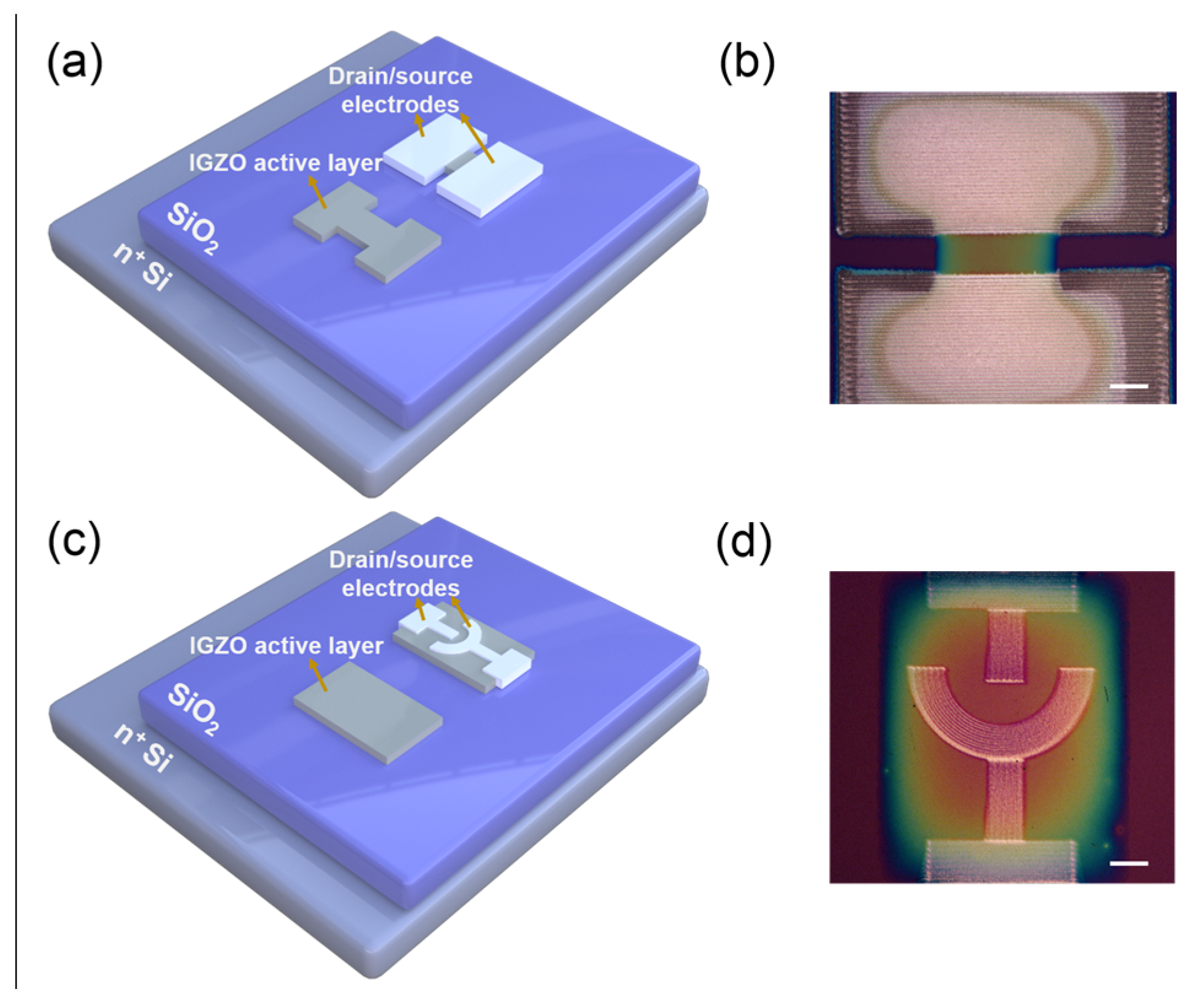
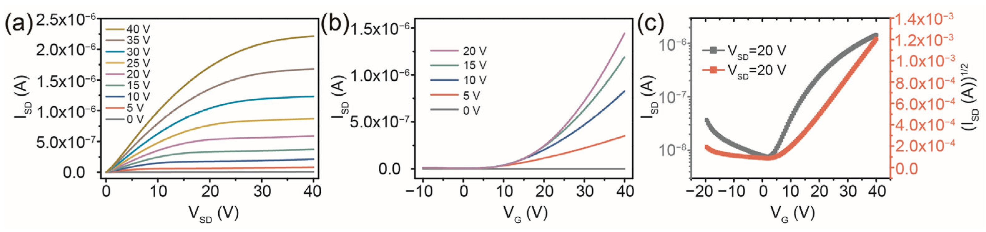
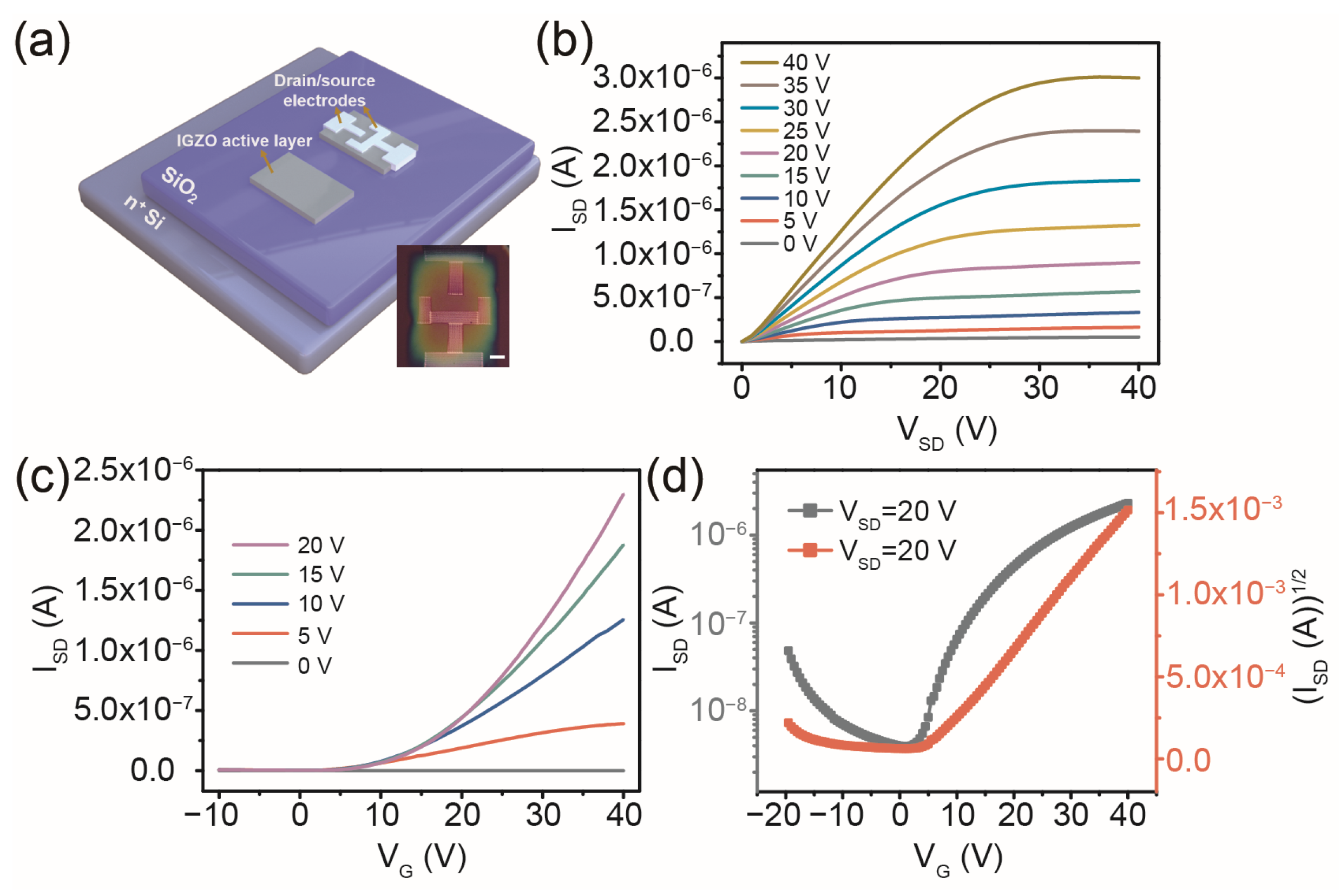
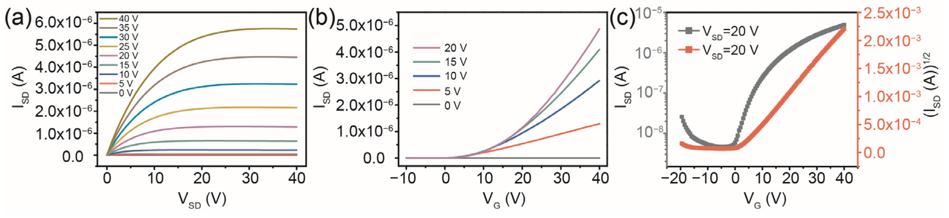
3. Results and Discussion

The patterned IGZO semiconductor layers were printed onto the Si/SiO2 substrates. In order to prevent cracks in the patterned IGZO, the annealing temperature of the pristine IGZO channel layer was set to 350 °C for 1 h, with a transition annealing step at 450 °C for 1 h, and finally annealing for 1 h at 550 °C in the air atmosphere with a heating rate of 5 °C/min. The thickness of the patterned IGZO semiconductor layer after annealing treatment was about 50 nm. The dumbbell shape of the IGZO semiconductor layers was designed to get more carrier injection when the drain–source voltage (VSD) was applied. The printed IGZO was covered with symmetrical rectangular source/drain electrodes to obtain a TFT with a rectangular channel pattern. Figure 2a shows the drain–source current (ISD) versus the VSD output characteristics of the IGZO TFT at gate voltages (VGS) from 0 to 40 V with the rectangular channel pattern. The curves show typical n-type field effect properties with an obvious transition from linear to saturation behavior in the IGZO channel. Figure 2b,c shows the transfer curves of the printed IGZO TFT with the rectangular channel. The threshold voltage (Vth) of ~6.1 V was estimated by extrapolating the linear portion of the (ISD)1/2 versus VG curves at VSD = 20 V in the typical transfer curves. The values of field effect mobility (μeff) and subthreshold swing (SS) were extracted from the transfer characteristics of the devices using the following formula:
μ eff = 2 L WC i ( I SD V G ) 2
SS = V G ( log 10 I SD )
where Ci is the capacitance of the SiO2 gate insulator with a thickness of about 285 nm per unit area, and L and W are the channel length and width of the patterned IGZO, respectively. The printed IGZO TFT with a rectangular channel exhibited a μeff value of 0.069 cm2 V−1 s−1, a SS of 8.6 V dec−1, and an on/off ratio (Ion/Ioff) of 1.8 × 10².
In contrast, we presented a structure of circular arc source/drain electrodes, which can solve the difference in electric field distribution between electrode centers and edges compared with a traditional structure of rectangular symmetry (see Figure 1b). The arc channel is more conducive to the effective injection of carriers through the source/drain electrodes. This was demonstrated by the value of the ISD in the output curves of the IGZO TFT with a circular arc channel pattern under a VG value of above 20 V, which was more than twice as large as that of a TFT with the rectangular symmetric source/drain electrodes at the corresponding VSD (see Figure 3a). From the representative transfer curves as shown in Figure 3b,c, the TFT device with a circular arc channel exhibits an n-type behavior with a Vth of ~2.2 V, a SS of 4.4 V dec−1, and an Ion/Ioff of 1.1 × 10³ at a VDS of 20 V. The geometrical factor as the effective channel length/width (L/W) of TFT devices with an arc channel can be expressed as follows [32,33]:
L W = ln ( R 2 / R 1 ) π
where R1 is the radius of the internal source electrode (~50 µm) and R2 is the sum of the radius of the internal source electrode and the length of the IGZO channel (~50 + 100 µm). By substituting the value of L/W into Equation (1), a μeff value of 0.208 cm2 V−1 s−1 was obtained for an IGZO TFT with the circular arc source/drain electrodes. The μeff value of the printed TFT was increased by two times with a circular arc IGZO channel. The value of Ion/Ioff increased by about an order of magnitude, which can more effectively reduce noise interference during TFT device operation. The reduction in the value of Vth can effectively reduce the power consumption of the printed TFTs. This was due to the fact that the uniformly distributed VSD promoted the efficient injection and migration of the carriers in the channel.
In contract, we changed the circular arc channel into a corresponding rectangular groove channel to verify the improvement of the field effect performance of the printed TFT devices (see Figure 4a). As shown in Figure 4b, the transition from the linear to the saturation regime and a good regulating effect on the ISD are observable in the output characteristics of the IGZO TFT with a structure of rectangular groove channels under different voltages. However, under the same VG, the value of ISD was smaller than that of the printed TFT with a circular arc channel and larger than that of the device with a rectangular symmetrical channel. This showed that the arc channel was not affected by the electrode tip on the potential distribution, and the plug-in structure of the source/drain electrodes was more conducive to carrier transport. Figure 4c,d illustrates the transfer characteristics of the IGZO TFT fabricated by ink-printing with a rectangular groove channel. The TFT device exhibited ~3.1 V Vth, 4.9 V dec−1 SS, and 5.9 × 10² Ion/Ioff at a VDS of 20 V. The channel L/W of this type of transistor was estimated using the following formula [34]:
L W = L a + 2 b
where L is the length of the channel; a and b are the width of the source electrode (~100 µm) and the distance between the two ends of the groove structure of the drain electrode and the source electrode (~100 + 200 µm), as shown in Figure 4a. By substituting the value of L/W into Equation (1), a μeff value of 0.093 cm2 V−1 s−1 was obtained for the IGZO TFT with a rectangular groove channel. Compared with TFT with a circular arc channel structure, this type of TFT device still has a certain gap in the performance of carrier regulation, which proves that the symmetry of potential distribution in the channel is helpful in improving the electrical properties of TFT devices. Finally, the field effect parameters of the TFT devices with various printed channel shapes are summarized in Table 1. Compared with the circular arc channel TFT, the other two types of TFT devices still have a certain gap in the performance of carrier regulation, which proves that the symmetry of potential distribution in the channel is helpful in improving the electrical properties of TFT devices. Compared with the mature TFTs, our printed preparation process still has a certain gap in the field effect characteristics, but we will improve the performance of the TFTs by modifying the interface next, especially to improve the problems that silver nanoparticles as electrodes will diffuse into the channel layer with the application of voltage and the defects at the interface between the channel layer and electrodes will affect the carrier transport.

4. Conclusions

We investigated a printing method to construct the bottom gate and top contact TFT devices with different IGZO channel patterns. We prepared an IGZO ink for printing with Ga, In, and Zn molar ratios of 1:2:7. A structure of a circle-arc channel was presented to solve the difference in electric field distribution between electrode centers and edges for TFTs. Compared with the traditional rectangular symmetrical and rectangular groove structures of source/drain electrodes for TFTs, the electrical performance of the device was significantly improved by introducing the circle-arc channel. The optimized printed TFT exhibited a Vth of ~2.2 V, a SS of ~4.4 V dec−1, an Ion/Ioff of ~1.1 × 10³, and a μeff value of 0.208 cm2 V−1 s−1. Among them, the Vth and μeff values are greatly increased, which is conducive to reducing the power consumption and improving the carrier regulation ability in printed TFT devices.

Author Contributions

Conceptualization, X.Y. (Xingzhen Yan) and B.L.; methodology, X.Y. (Xingzhen Yan), B.L. and Y.Z.; formal analysis, B.L. and Y.Z.; investigation, Y.W. and C.W.; writing—original draft preparation, X.Y. (Xingzhen Yan); writing—review and editing, X.Y. (Xingzhen Yan) and X.Y. (Xiaotian Yang); project administration, Y.C. and X.Y. (Xiaotian Yang); funding acquisition, X.Y. (Xingzhen Yan). All authors have read and agreed to the published version of the manuscript.

Funding

This work is supported by the Science and Technology Development Project of Jilin Province, China (Nos. YDZJ202201ZYTS396, JJKH20220271KJ, and JJKH20240364KJ) and the National Key R&D Program of Strategic Advanced Electronic Materials of China (No. 2022YFB3603802).

Data Availability Statement

Data are contained within the article.

Conflicts of Interest

The authors declare no conflict of interest.

References

  1. Nomura, K.; Ohta, H.; Ueda, K.; Kamiya, T.; Hirano, M.; Hosono, H. Thin–film transistor fabricated in single-crystalline transparent oxide semiconductor. Science 2003, 300, 1269–1272. [Google Scholar] [CrossRef] [PubMed]
  2. Gelinck, G.; Huitema, H.; Veenendaal, E.; Cantatore, E.; Schrijnemakers, L.; Putten, J.; Geuns, T.; Beenhakkers, M.; Giesbers, J.; Huisman, B.; et al. Flexible active-matrix displays and shift registers based on solution-processed organic transistors. Nat. Mater. 2004, 3, 106–110. [Google Scholar] [CrossRef] [PubMed]
  3. Dimitrakopoulos, C.D.; Purushothaman, S.; Kymissis, J.; Callegari, A.; Shaw, J.M. Low–Voltage Organic Transistors on Plastic Comprising High-Dielectric Constant Gate Insulators. Science 1999, 283, 822–824. [Google Scholar] [CrossRef]
  4. Fortunato, E.; Barquinha, P.; Pimentel, A.; Goncalves, A.; Marque, A.; Pereira, L.; Martins, R. Wide-Bandgap High-Mobility ZnO Thin-Film Transistors Produced at Room Temperature. Appl. Phys. Lett. 2004, 85, 2541–2543. [Google Scholar] [CrossRef]
  5. Tang, Y.; Huang, C.H.; Nomura, K. Vacuum-Free Liquid-Metal-Printed 2D Indium-Tin Oxide Thin-Film Transistor for Oxide Inverters. ACS Nano 2022, 16, 3280–3289. [Google Scholar] [CrossRef]
  6. Jana, S.; Martins, R.; Fortunato, E. Stacking-Dependent Electrical Transport in a Colloidal CdSe Nanoplatelet Thin-Film Transistor. Nano Lett. 2022, 22, 2780–2785. [Google Scholar] [CrossRef] [PubMed]
  7. Wu, L.; Dong, Z.C.; Li, F.Y.; Zhou, H.H.; Song, Y.L. Emerging Progress of Inkjet Technology in Printing Optical Materials. Adv. Opt. Mater. 2016, 4, 1915–1932. [Google Scholar] [CrossRef]
  8. Avis, C.; Hwang, H.R.; Jang, J. Effect of Channel Layer Thickness on the Performance of Indium–Zinc–Tin Oxide Thin Film Transistors Manufactured By Inkjet Printing. Appl. Mater. Interfaces 2014, 6, 10941–10945. [Google Scholar] [CrossRef] [PubMed]
  9. Fortunato, E.; Barquinha, P.; Martins, R. Oxide Semiconductor Thin-Film Transistors: A Review of Recent Advances. Adv. Mater. 2012, 24, 2945–2986. [Google Scholar] [CrossRef] [PubMed]
  10. Rim, Y.S.; Chen, H.J.; Kou, X.L.; Duan, H.S.; Zhou, H.P.; Cai, M.; Kim, H.J.; Yang, Y. Boost up mobility of solution–processed metal oxide thin–film transistors via confining structure on electron pathways. Adv. Mater. 2014, 26, 4273–4278. [Google Scholar] [CrossRef]
  11. Scheideler, W.J.; Subramanian, V. How to print high-mobility metal oxide transistors—Recent advances in ink design processing, and device engineering. Appl. Phys. Lett. 2022, 121, 220502. [Google Scholar] [CrossRef]
  12. Park, J.W.; Kang, B.H.; Kim, H.J. A Review of Low-Temperature Solution-Processed Metal Oxide Thin-Film Transistors for Flexible Electronics. Adv. Funct. Mater. 2020, 30, 1904632. [Google Scholar] [CrossRef]
  13. Hamlin, A.B.; Ye, Y.; Huddy, J.E.; Rahman, M.S.; Scheideler, W.J. 2D transistors rapidly printed from the crystalline oxide skin of molten indium. npj 2D Mater. Appl. 2022, 6, 16. [Google Scholar] [CrossRef]
  14. Liu, F.; Gillan, L.; Leppaniemi, J.; Alastalo, A. Focused Review on Print-Patterned Contact Electrodes for Metal-Oxide Thin-Film Transistors. Adv. Mater. Interfaces 2023, 10, 2202258. [Google Scholar] [CrossRef]
  15. Fukuda, K.; Takeda, Y.; Yoshimura, Y.; Shiwaku, R.; Tran, L.T.; Sekine, T.; Mizukami, M.; Kumaki, D.; Tokito, S. Fully-printed high-performance organic thin-film transistors and circuitry on one-micron-thick polymer films. Nat. Commun. 2014, 5, 4147. [Google Scholar] [CrossRef]
  16. Ruiz-Preciado, L.A.; Baek, S.; Strobel, N.; Xia, K.; Seiberlich, M.; Park, S.; Lemmer, U.; Jung, S.; Hernandez-Sosa, G. Monolithically printed all-organic flexible photosensor active matrix. npj Flexible Electron. 2023, 7, 6. [Google Scholar] [CrossRef]
  17. Cao, C.; Andrews, J.B.; Kumar, A.; Franklin, A.D. Improving contact interfaces in fully printed carbon nanotube thin–film transistors. ACS Nano 2016, 10, 5221–5229. [Google Scholar] [CrossRef]
  18. Ha, J.; Yoo, H.; Seo, J.; Yoon, J.; Hong, Y. Photoresponse Analysis of All-Inkjet-Printed Single-Walled Carbon Nanotube Thin-Film Transistors for Flexible Light-Insensitive Transparent Circuit Applications. ACS Appl. Mater. Interfaces 2023, 15, 3192–3201. [Google Scholar] [CrossRef] [PubMed]
  19. Kuribara, K.; Wang, H.; Uchiyama, N.; Fukuda, K.; Yokota, T.; Zschieschang, U.; Jaye, C.; Fischer, D.; Klauk, H.; Yamamoto, T.; et al. Organic transistors with high thermal stability for medical applications. Nat. Commun. 2012, 3, 723. [Google Scholar] [CrossRef]
  20. Gillan, L.; Li, S.; Lahtinen, J.; Chang, C.H.; Alastalo, A.; Leppaniemi, J. Inkjet-Printed Ternary Oxide Dielectric and Doped Interface Layer for Metal-Oxide Thin-Film Transistors with Low Voltage Operation. Adv. Mater. Interfaces 2021, 8, 2100728. [Google Scholar] [CrossRef]
  21. Divya, M.; Pradhan, J.R.; Priyadarsini, S.S.; Dasgupta, S. High Operation Frequency and Strain Tolerance of Fully Printed Oxide Thin Film Transistors and Circuits on PET Substrates. Small 2022, 18, 2202891. [Google Scholar] [CrossRef] [PubMed]
  22. Lee, Y.G.; Choi, W.S. Effect of PGMEA Addition on Zinc-Tin-Oxide Thin-Film Transistor Fabricated by Inkjet-Printing Process. Adv. Eng. Mater. 2022, 24, 2200128. [Google Scholar] [CrossRef]
  23. Wang, R.; Liang, K.; Wang, S.; Cao, Y.; Xin, Y.; Peng, Y.; Ma, X.; Zhu, B.; Wang, H.; Hao, Y. Printable Epsilon-Type Structure Transistor Arrays with Highly Reliable Physical Unclonable Functions. Adv. Mater. 2023, 35, 2210621. [Google Scholar] [CrossRef]
  24. Liang, K.; Wang, R.; Ren, H.; Li, D.; Tang, Y.; Wang, Y.; Chen, Y.; Song, C.; Li, F.; Liu, G.; et al. Printable Coffee-Ring Structures for Highly Uniform All Oxide Optoelectronic Synaptic Transistors. Adv. Opt. Mater. 2022, 10, 2201754. [Google Scholar] [CrossRef]
  25. Secor, E.B.; Smith, J.; Marks, T.J.; Hersam, M.C. High-performance inkjet-printed indium-gallium-zinc-oxide transistors enabled by embedded, chemically stable graphene electrodes. ACS Appl. Mater. Interfaces 2016, 8, 17428–17434. [Google Scholar] [CrossRef]
  26. Kim, W.G.; Tak, Y.J.; Yoo, H.; Kim, H.T.; Park, J.W.; Choi, D.H.; Kim, H.J. Photo-induced Reactive Oxygen Species Activation for Amorphous Indium-Gallium-Zinc Oxide Thin-Film Transistors Using Sodium Hypochlorite. ACS Appl. Mater. Interfaces 2021, 13, 44531–44540. [Google Scholar] [CrossRef] [PubMed]
  27. Nomura, K.; Ohta, H.; Takagi, A.; Kamiya, T.; Hirano, M.; Hosono, H. Room–Temperature Fabrication of Transparent Flexible Thin–Film Transistors Using Amorphous Oxide Semiconductors. Nature 2004, 432, 488–492. [Google Scholar] [CrossRef]
  28. Chen, R.; Lan, L. Solution–processed metal–oxide thin–film transistors: A review of recent developments. Nanotechnology 2019, 30, 312001. [Google Scholar] [CrossRef]
  29. Shao, S.; Wang, S.; Li, M.; Xie, T.; Fang, Y.; Guo, P.; Chen, Z.; Zhao, J. 75 kbit printed indium oxide (IO)/indium gallium zinc oxide (IGZO) heterojunction photoelectric synaptic transistor arrays for an artificial visual memory system. J. Mater. Chem. C 2023, 11, 7019. [Google Scholar] [CrossRef]
  30. Yan, X.; Li, B.; Song, K.; Zhang, Y.; Wang, Y.; Yang, F.; Wang, C.; Chi, Y.; Yang, X. Fabrication and properties of InGaZnO thin-film transistors based on sol-gel method with different electrode patterns. Micromachines 2022, 13, 2207. [Google Scholar] [CrossRef]
  31. Jang, J.; Kang, H.; Chakravarthula, H.C.N.; Subramanian, V. Fully Inkjet-Printed Transparent Oxide Thin Film Transistors Using a Fugitive Wettability Switch. Adv. Electron. Mater. 2015, 1, 1500086. [Google Scholar] [CrossRef]
  32. Munteanu, D.; Cristoloveanu, S.; Hovel, H. Circular pseudo-metal oxide semiconductor field effect transistor in silicon-on-insulator. Electrochem. Solid-State Lett. 1999, 2, 242–243. [Google Scholar] [CrossRef]
  33. Zhao, C.; Fung, T.C.; Kanicki, J. Half-Corbino short-channel amorphous In-Ga-Zn-O thin-film transistors with a-SiOx or a-SiOx/a-SiNx passivation layers. Solid-State Electron. 2016, 120, 25–31. [Google Scholar] [CrossRef]
  34. Lee, H.; Yoo, G.; Yoo, J.S.; Kanicki, J. Asymmetric electrical properties of fork a-Si:H thin-film transistor and its application to flat panel displays. J. Appl. Phys. 2009, 105, 124522. [Google Scholar] [CrossRef]
Figure 1. Schematic illustrations of the procedures for fabricating printed IGZO TFTs with the symmetrical rectangular source/drain electrodes (a) and circular arc source/drain electrodes (c). Microscope images of the rectangular (b) and circular arc channel patterns (d) of IGZO/SiO2/Si TFTs. The scale bar is 100 μm.
Micromachines 14 02121 g001
Figure 2. (a) Output characteristics of a printed IGZO TFT with symmetrical rectangular source/drain electrodes. (b,c) Transfer characteristics of the rectangular channel IGZO TFT.
Micromachines 14 02121 g002
Figure 3. (a) Output characteristics of a printed IGZO TFT with the circular arc source/drain electrodes. (b,c) Transfer characteristics of the circular arc channel IGZO TFT.
Micromachines 14 02121 g003
Figure 4. (a) Schematic illustration of fabrication of a printed IGZO TFT with a rectangular groove channel. The insert shows a microscope image of an IGZO/SiO2/Si TFT with a rectangular channel pattern. The scale bar is 100 μm. (b) Output characteristics of the printed IGZO TFT with the rectangular groove channel. (c,d) Transfer characteristics of the rectangular groove channel IGZO TFT.
Micromachines 14 02121 g004
Table 1. The field effect parameters of the TFTs with various printed channel shapes.
TypeOn/Off RatioField Effect Mobility
(cm2 V−1 s−1)
Threshold
Voltage (V)
Symmetrical rectangular channel1.8 × 1020.0696.1
Rectangular groove channel5.9 × 1020.0933.1
Circular arc channel1.1 × 1030.2082.2
Disclaimer/Publisher’s Note: The statements, opinions and data contained in all publications are solely those of the individual author(s) and contributor(s) and not of MDPI and/or the editor(s). MDPI and/or the editor(s) disclaim responsibility for any injury to people or property resulting from any ideas, methods, instructions or products referred to in the content.

