Article

Excitation of Hybrid Waveguide-Bloch Surface States with Bi2Se3 Plasmonic Material in the Near-Infrared Range

1
School of Electronics Engineering, Nanjing Xiaozhuang University, Nanjing 211171, China
2
Jiangsu Collaborative Innovation Center on Atmospheric Environment and Equipment Technology (CICAEET), Nanjing University of Information Science & Technology, Nanjing 210044, China
*
Author to whom correspondence should be addressed.
Micromachines 2022, 13(7), 1020; https://doi.org/10.3390/mi13071020
Submission received: 9 June 2022 / Revised: 24 June 2022 / Accepted: 27 June 2022 / Published: 28 June 2022
(This article belongs to the Section A:Physics)

Abstract

:
Bloch surface waves (BSWs) with Bi2Se3 in a composite structure consisting of a coupling prism, distributed Bragg reflector (DBR) and cavity layer have been demonstrated. The design relies on the confinement of surface waves that originates from the coupling between the defective layer of plasmonic material (Bi2Se3) and DBR. The presence of the cavity layer modifies the local effective refractive index, enabling direct manipulation of the BSWs. The transfer matrix method (TMM) is used to evaluate the reflectance and absorptance responses in the spectral domain for various angles of incidence, demonstrating the presence of sharp resonances associated with the BSW. With an optimal thickness of DBR bilayers, the energy of an evanescent wave can be transferred into the periodic stack resulting in the excitation of waveguide modes (WGMs). It is believed that the proposed design possesses the advantage in terms of easy fabrication to develop integrated photonic systems, especially for biological and chemical sensing.

1. Introduction

During the past decades, significant attention has been paid to platforms that can support electromagnetic surface waves (EMSWs) [1,2,3,4]. Among the various methods and structures, BSWs are the modes propagating at the interface between the dielectric multilayer and external medium decay exponentially inside the multilayers due to the presence of the photonic band gap (PBG). The BSW field distributions can be tuned by tailoring the thickness and material of the topmost layer, which enables the investigation of interactions with external media. BSW-based sensors have been proved can provide several advantages compared to surface plasmon polaritons (SPPs)-based sensors [5,6,7]. Firstly, BSWs can be excited under both polarizations and any wavelength by changing the composition and parameters of the DBR suitably. In addition, BSWs exhibit much sharper resonances than conventional surface plasmon resonance (SPR) [8,9]. Moreover, the multilayer structure can be fabricated without any pattern, making BSW an attractive optical sensing tool [10,11,12].
With the preparation and development of new materials, the performance of optical devices can be significantly improved [13,14,15,16,17,18]. Tetradymites have become popular due to the recently discovered topological insulator property [19,20]. Bismuth selenide (Bi2Se3) has been shown as one of the potential candidates for surface plasmons [21,22], which holds great potential in high-performance photonic devices [23,24,25]. At the same time, a Bi2Se3 topological insulator is easy to prepare at a low cost and can even achieve saturable absorption because of its unique physical properties [18]. Thus far, most of the research are concerned with realizing narrow and tunable resonance based on BSW, but it is rarely reported that the tunable and multichannel BSWs can be achieved simultaneously. Moreover, a novel Bi2Se3 platform for the excitation of BSWs is significant for two-dimensional integrated photonics.
The presented work shows the possibility of using a Bi2Se3–DBR composite structure for the excitation of BSWs. Angle dependence of the reflection and absorption spectra is studied through TMM. It is also found that the BSW response is strongly dependent on the thickness of the Bragg mirror layer, incident angle and refractive index of the prism. In addition, manipulating the reflection dips can be achieved by changing the thickness of the cavity layer. More importantly, the proposed design possesses the advantage in terms of easy fabrication and planar multilayer system, which holds great potential in efficient narrowband filters as well as beam splitters and deflectors.

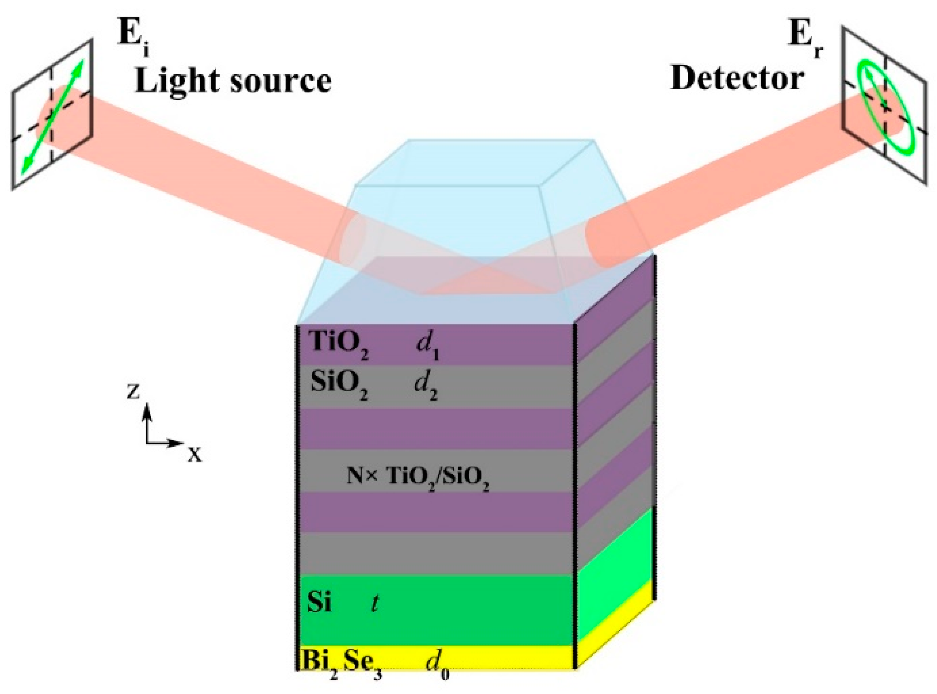
2. Materials and Methods

The sample used for the BSW excitation consisted of a DBR and a Si cavity layer with a thin Bi2Se3 layer deposited on the top. As depicted in Figure 1, the DBR is composed of N pairs of alternately stacked TiO2 (~96 nm) and SiO2 (~172 nm) thin films deposited onto a prism substrate by means of ion beam sputtering. The incident light impinges on the structure from the prism with an angle of θ. d0, d1, d2, and t stand for the thicknesses of Bi2Se3, TiO2, SiO2, and cavity layer Si, respectively. The period number of TiO2/SiO2 Bragg mirror is set as N. At the wavelengths of interest, the refractive index for Si is fixed at 3.45.
Wavelength-dependent refractive indices for TiO2 [26] and SiO2 [27] as the high and low refractive index materials at a certain wavelength λ are given by:
n TiO 2 = 5.931 + 0.2441 λ 2 0.0803
n TiO 2 = 1 + 0.6962 λ 2 λ 2 0.0684 2 + 0.4079 λ 2 λ 2 0.1162 2 + 0.8975 λ 2 λ 2 9.8961 2
The number of periods for DBR is N; the entire device is supposed to be fabricated on a prism substrate. The monochromatic plane wave with an electric field parallel to the y-axis is called transverse electric (TE) polarization. Bi2Se3 has attracted great attention due to its hyperbolic behavior in the near-infrared to visible spectrum [21]. Accurately modeling the permittivity is vital for evaluating the optical response in Bi2Se3-based optoelectronic applications. The real and imaginary parts of the dielectric function on an ac-facet and ab-facet are obtained from Ref. [21], which is shown in Figure 2.
We simulate plane wave interactions with such planar multi-layer structures by using the semi-analytical transfer matrix method (TMM) [14,28,29]:
E o u t = M E i n
where Eout is the electric field of the output side, Ein is the electric field of the incident light, and M is the transfer matrix of the whole structure, which can be expressed as follows:
M = ( M 11 M 21 M 12 M 22 ) = ( m TiO 2 m SiO 2 ) N m Si m Bi 2 Se 3
where m TiO 2 , m SiO 2 , mSi and m Bi 2 Se 3 are the transmission matrix of light passing through each layer, and N is the period number of DBR.
The transmission matrix of incident light in each layer can be expressed as:
m i = [ cos δ i i p i sin δ i i p i 1 sin δ i cos δ i ]
where δi = (2π/λ)nidicosθi, nidi is the optical thickness of the corresponding layer, θi is the angle between the light in the dielectric layer and the normal direction of the interface, and λ is the wavelength of the incident light. pi has the following formulas for TE and TM polarization, respectively:
p i T E = n i ε 0 μ 0 cos θ i
p i T M = n i ε 0 μ 0 / cos θ i
where i = m TiO 2 , m SiO 2 , mSi or m Bi 2 Se 3 , ε0 and μ0 are the permeability of vacuum dielectric constant and vacuum dielectric constant, respectively.
The reflection (R) and the transmission (T) of light can be expressed as:
R = | ( M 11 + M 12 ) p i ( M 21 + M 22 p T ) ( M 11 + M 12 ) p i + ( M 21 + M 22 p T ) | 2
T = | 2 p i ( M 11 + M 12 p T ) p i + ( M 21 + M 22 p T ) | 2
where subscript i and T represent the incident and transmission space, respectively. The absorbance can be deduced through A = 1 − RT.

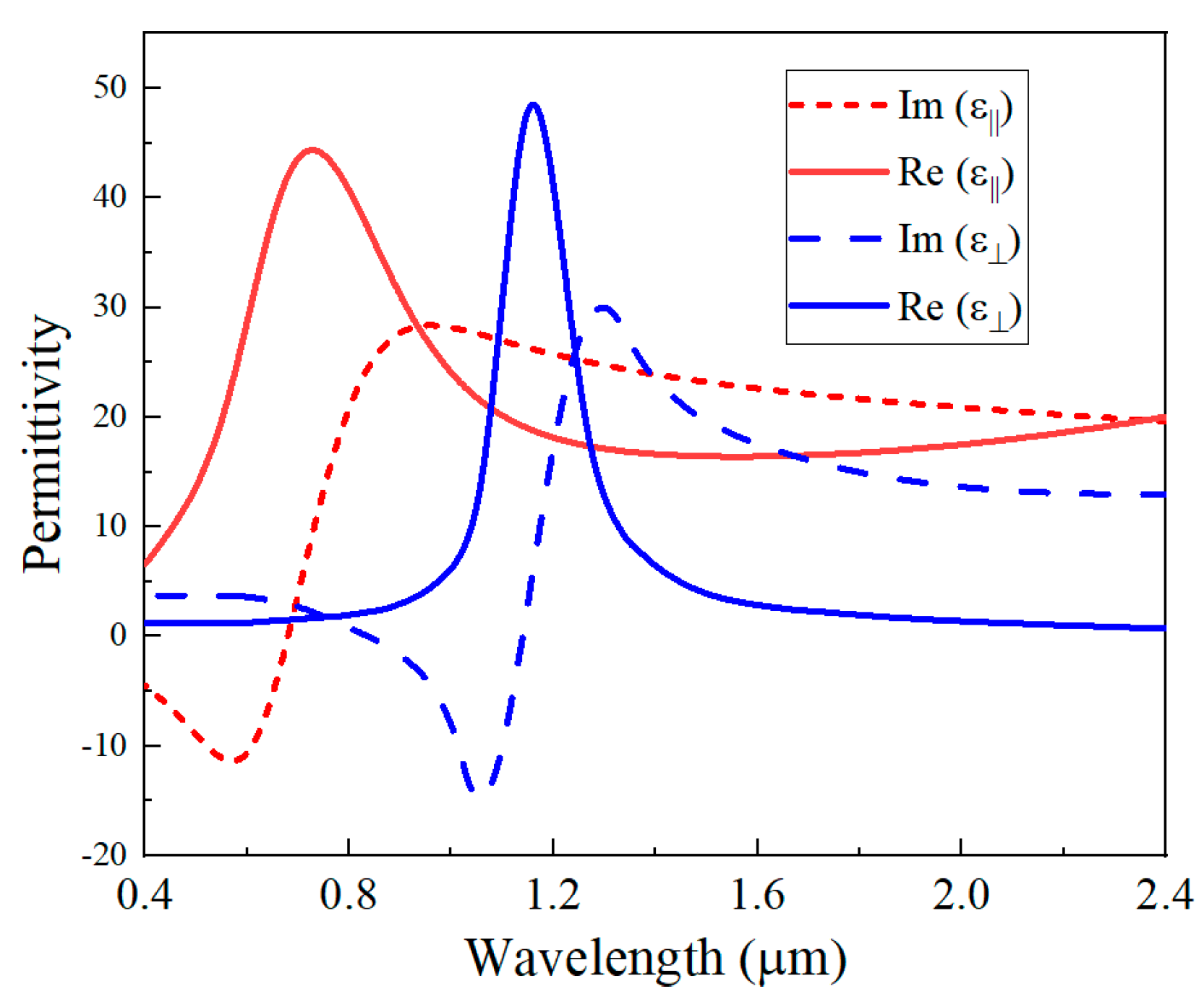
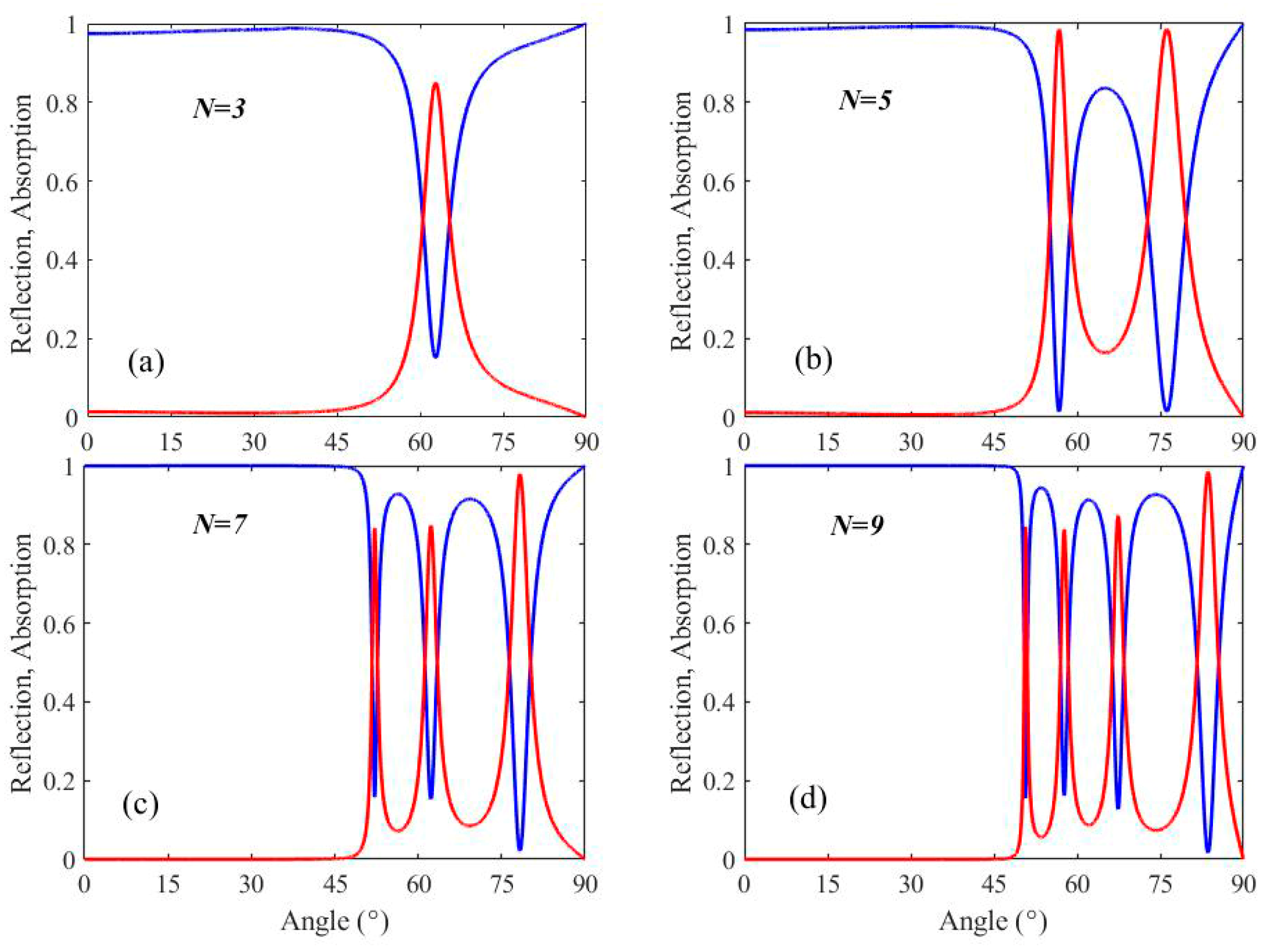
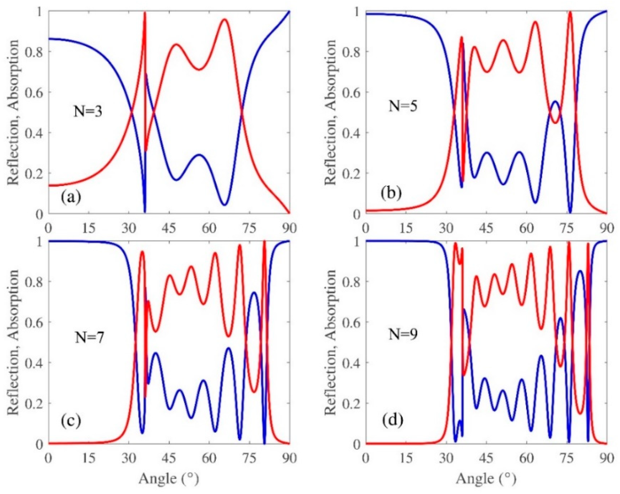
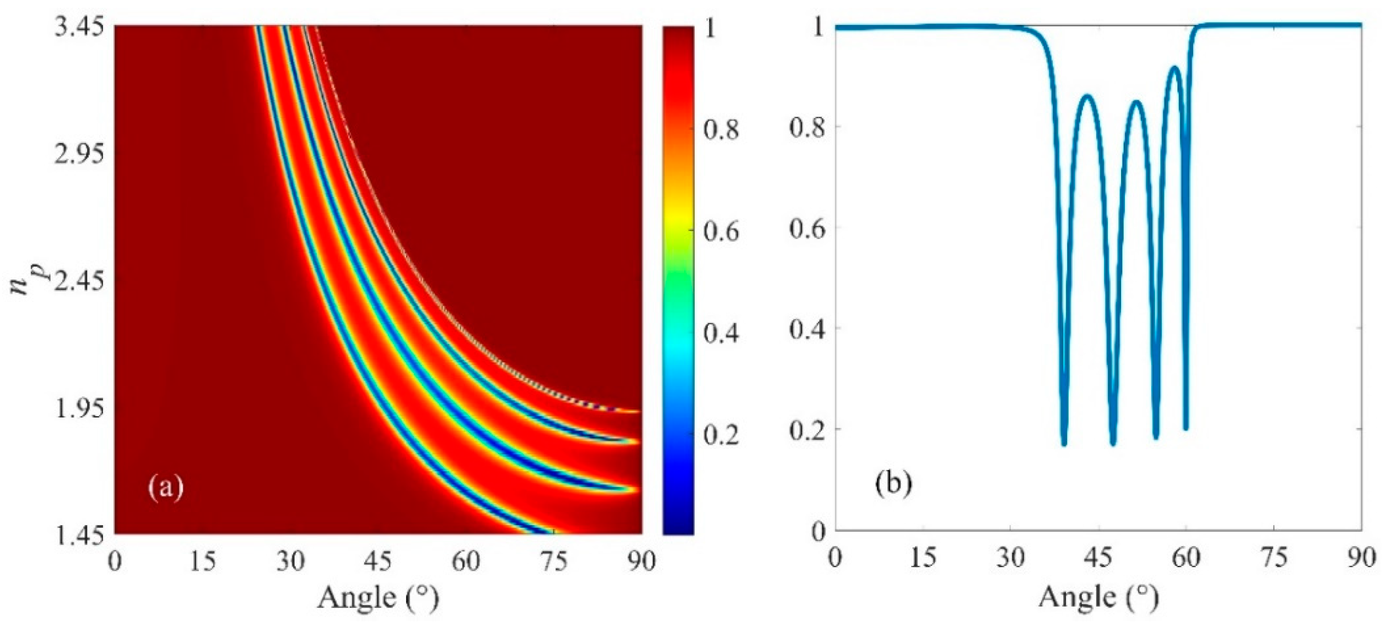
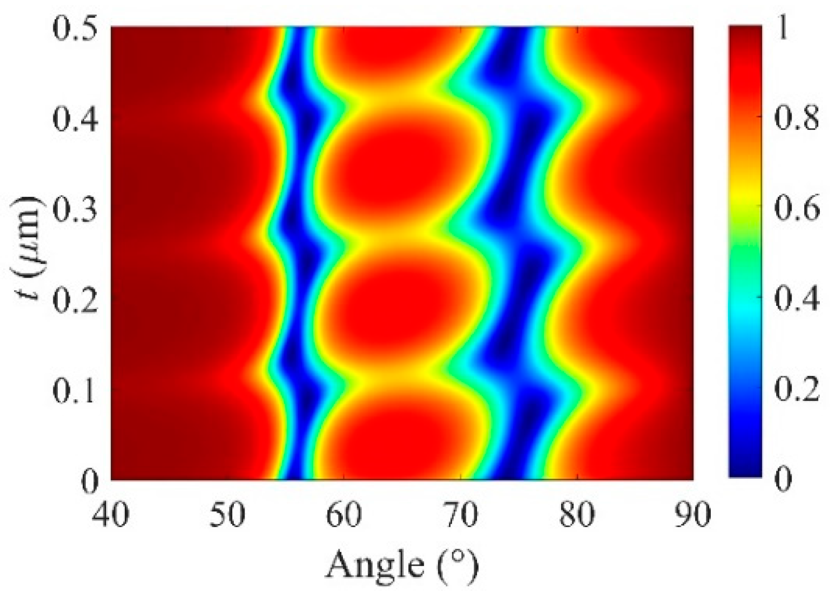
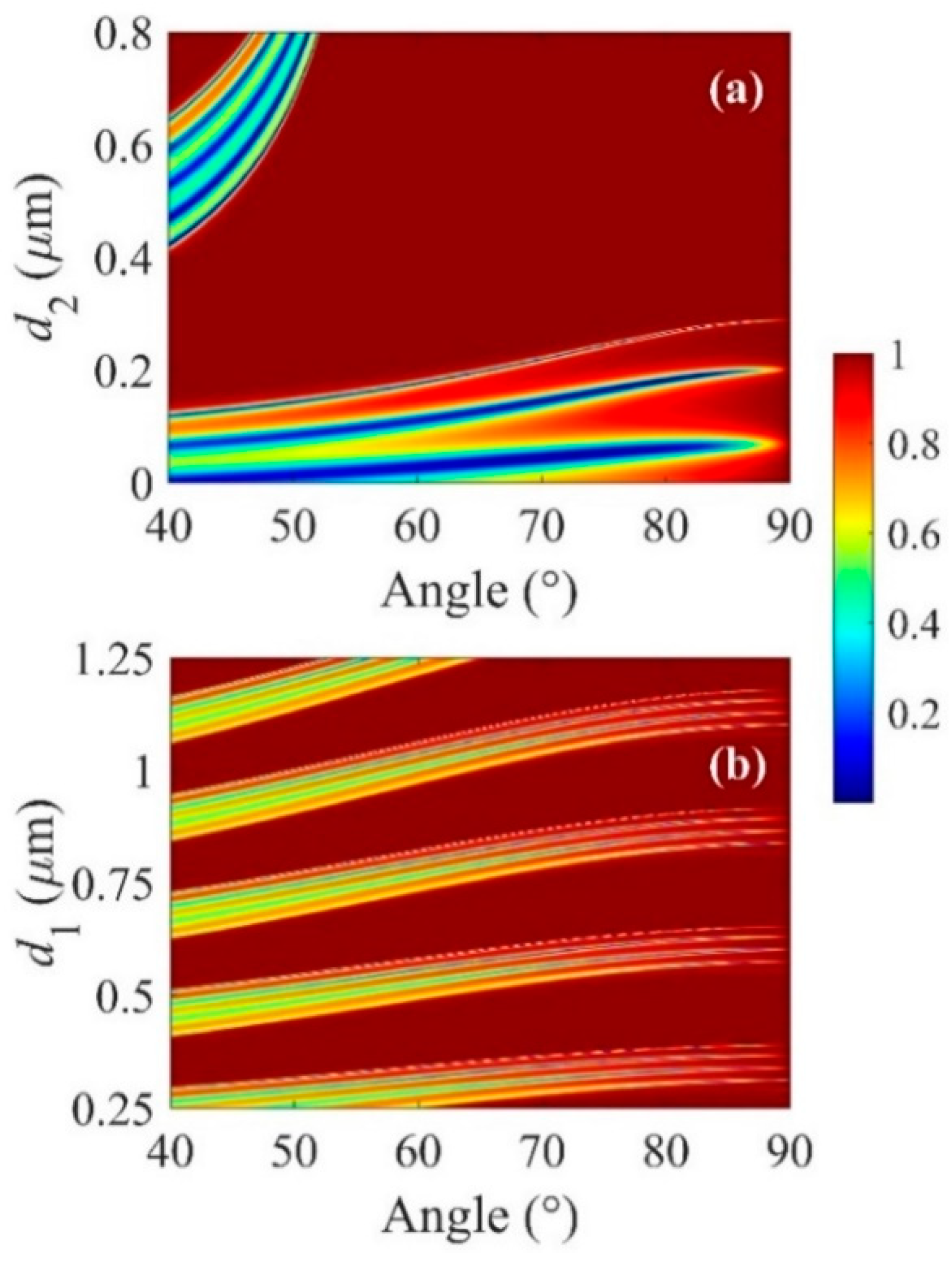
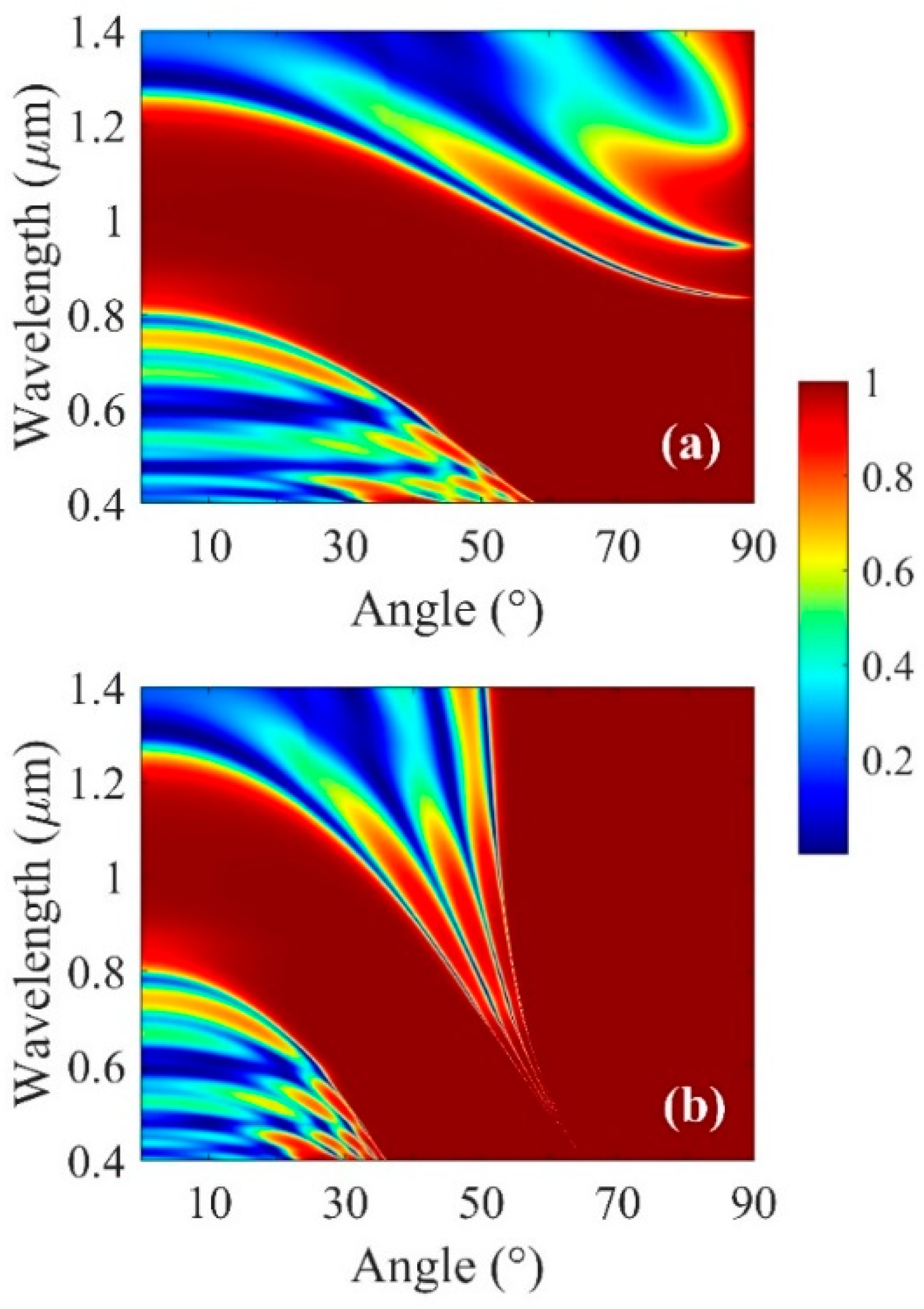
3. Results and Analysis

A possibility of the excitation of surface waves using an evanescent field in a DBR geometry is highly favorable. We first study the Bi2Se3/DBR integrated with a prism to examine the role of BSW resonance. Figure 3a plots the optical responses (absorption and reflection spectra) of the hybrid DBR system consisting of three pairs (N = 3) of TiO2/SiO2. The conditions of Bragg conditions are met by selecting a quarter optical thickness of the DBR resonant wavelength for TiO2 and SiO2 layers. The thickness of the Bi2Se3 layer is 25 nm, and Si is chosen with a thickness of 80 nm as the cavity. It is clear that a deep reflection dip appears under 62.6° at the resonance wavelength of 1000 nm), indicating the BSW excitation at the Bi2Se3/air interface. With the increase of the number of periodic layers N, the absorption peaks of the structure gradually change, as shown in Figure 3b–d. When the angle of incident light is greater than the total reflection critical angle, an evanescent wave arising from total internal reflection (TIR) is formed. With an optimal thickness of TiO2/SiO2 bilayers, the energy of an evanescent wave can be transferred into the periodic stack resulting in the excitation of waveguide modes (WGMs). Thus, when the number N increases from three to nine pairs continuously, more absorption peaks appear.
Figure 4a–d show the reflection and absorption spectra with different N for TE polarization. It is evident that more resonance will appear with the increasing N. Reflection dips have been observed and are considered as the WGMs, and the incident waves are well localized within the DBR mirror. The different dips in the spectrum are related to the different order of guiding modes inside the multilayers. In the following study, we will restrict the study to a TE polarization monochromatic plane wave.
In addition to the number of DBR pairs, the dependence of optical reflection on the refractive index of the prism is also investigated, as depicted in Figure 5a,b, respectively. It is a key point that our design can achieve TIR, and the critical angle can be calculated θ c = arcsin ( n e f f / n p ) according to Snell’s law. neff is defined as the effective refractive index of TiO2/SiO2 pairs. Figure 5a shows the reflectance spectra of the structure for the TE waves at different np and angles θ of incidence of the radiation onto the structure. It is evident that with a larger refractive index, more resonance can occur with the blue shift of the resonance angles. The reflectivity spectrum undergoes four pronounced reflection dips at 39.23°, 47.65°, 54.92° and 59.89°, which suggests that multiple BSW states are excited simultaneously when np = 2.45 is in the near-infrared region.
To explore the physics mechanism of the existence of BSW states, a comprehensive reflectivity map, which is on the plane of incident angle and thickness of cavity layer (t), is illustrated in Figure 6. It is interesting to observe that the resonance of BSW is continuously variable with t, and the interval between the two neighboring stripes strictly equals λ/2nSi for a given wavelength λ.
The propagation properties of the BSW mode on the platform can be altered by changing the thickness of the DBR layer. Their thicknesses define the location of the dispersion line in the band gap of the multilayers. Variation of reflection in the proposed geometry as a function of d1 and d2 when λcentral = 1 μm. For the tunability of the working wavelength, we break the constraint that the optical thickness of the SiO2 and TiO2 layer is a quarter of λcentral. It is clear from Figure 7a that, with a fixed d1 (96 nm), as d2 increases to 800 nm, the device shows two bands of resonance with minimum reflection. This multiband response of the device increases the flexibility of the device preparation at a targeted wavelength. With a fixed d2 (172 nm), as d1 increases from 0.25 μm to 1.25 μm, multiple band gaps appear in the reflection map (shown in Figure 7b). Overall, it is convenient for one to obtain targeted optical responses by adjusting the thicknesses of planar films in DBR.
In Figure 8, the numerical experimental angle-resolved reflection spectra in the wavelength range 0.4–1.4 μm and incident angle 0–90° are shown for different prism refractive indices. We observe several optical modes that indicate the presence and location of a PBG of the multilayer structure. The BSW modes are excited because of the surface defect. Although such modes are intrinsically present at Bi2Se3–air interfaces, they are non-radiative in nature, as their momentum is larger than the free-space wave momentum [30,31]. Thus, we use a prism to provide additional momentum to the incident wave to excite BSWs.

4. Conclusions

In summary, we have demonstrated an angle-interrogated BSW device structure by exploiting the surface properties by introducing a Bi2Se3 layer on top of a prism-coupled photonic crystal. Comprehensive investigations regarding the effects of the structural parameters on the reflection and absorption properties have been conducted. The number of periodic layers N plays an important role in the occurrence of multiple BSWs in this structure. It was also found that the BSW response is strongly dependent on the thickness of the cavity layer, Bragg mirror layer, light incident angle and refractive index of the prism. Compared with other BSW-based devices of different types, it is shown that the proposed interfaces can support bound surface modes that differ significantly from the surface plasmon polaritons. These devices can be applied as efficient narrowband filters, beam splitters, and deflectors and also extend the usage of Bi2Se3.

Author Contributions

Conceptualization, H.L. and G.Z.; methodology, G.Z.; software, H.L.; investigation, H.L. and G.Z.; writing—original draft preparation, H.L.; writing—review and editing, G.Z.; funding acquisition, G.Z. All authors have read and agreed to the published version of the manuscript.

Funding

This research was funded by the Natural Science Foundation of the Jiangsu Province, grant number (BK20191396).

Conflicts of Interest

The authors declare no conflict of interest.

References

  1. Cong, J.; Liu, W.; Zhou, Z.; Ren, N.; Ding, G.; Chen, M.; Yao, H. Sub-nanometer linewidth perfect absorption in visible band induced by Bloch surface wave. Opt. Mater. 2016, 62, 261–266. [Google Scholar] [CrossRef]
  2. Hlubina, P.; Gryga, M.; Ciprian, D.; Pokorny, P.; Gembalova, L.; Sobota, J. High performance liquid analyte sensing based on Bloch surface wave resonances in the spectral domain. Opt. Laser Technol. 2022, 145, 107492. [Google Scholar] [CrossRef]
  3. Gryga, M.; Vala, D.; Kolejak, P.; Gembalova, L.; Ciprian, D.; Hlubina, P. One-dimensional photonic crystal for Bloch surface waves and radiation modes-based sensing. Opt. Mater. Express 2019, 9, 4009–4022. [Google Scholar] [CrossRef]
  4. Bashiri, J.; Rezaei, B. Controlled switching of the optical surface waves in one-dimensional photonic crystals containing left-handed materials in the presence of a chiral metamaterial as a cap layer. Photonic Nanostruct. 2021, 43, 100891. [Google Scholar] [CrossRef]
  5. Sinibaldi, A.; Danz, N.; Descrovi, E.; Munzert, P.; Schulz, U.; Sonntag, F.; Dominici, L.; Michelotti, F. Direct comparison of the performance of Bloch surface wave and surface plasmon polariton sensors. Sens. Actuators B Chem. 2012, 174, 292–298. [Google Scholar] [CrossRef]
  6. Lereu, A.L.; Zerrad, M.; Passian, A.; Amra, C. Surface plasmons and Bloch surface waves: Towards optimized ultra-sensitive optical sensors. Appl. Phys. Lett. 2017, 111, 011107. [Google Scholar] [CrossRef]
  7. Gryga, M.; Ciprian, D.; Gembalova, L.; Hlubina, P. Sensing based on Bloch surface wave and self-referenced guided mode resonances employing a one-dimensional photonic crystal. Opt. Express 2021, 29, 12996–13010. [Google Scholar] [CrossRef]
  8. Baghbadorani, H.K.; Barvestani, J.; Entezar, S.R. Biosensors based on Bloch surface waves in one-dimensional photonic crystal with graphene nanolayers. Appl. Opt. 2017, 56, 462–469. [Google Scholar] [CrossRef]
  9. Gonzalez-Valencia, E.; Villar, I.D.; Torres, P. Bloch waves at the surface of a single-layer coating D-shaped photonic crystal fiber. Opt. Lett. 2020, 45, 2547–2550. [Google Scholar] [CrossRef]
  10. Ma, J.P.; Kang, X.-B.; Wang, Z.-G. Sensing performance optimization of the Bloch surface wave biosensor based on the Bloch impedance-matching method. Opt. Lett. 2018, 43, 5375–5378. [Google Scholar] [CrossRef]
  11. Zhang, C.; Liu, Q.; Peng, X.; Ouyang, Z.; Shen, S. Sensitive THz sensing based on Fano resonance in all-polymeric Bloch surface wave structure. Nanophotonics 2021, 10, 3879–3888. [Google Scholar] [CrossRef]
  12. Gan, S.; Wang, H.; Liang, J.; Dai, X.; Xiang, Y. Ultra-Sensitive Refractive Index Sensors Based on Bloch Surface Waves with Transition Metal Dichalcogenides. IEEE Sens. J. 2019, 19, 8675–8680. [Google Scholar] [CrossRef]
  13. Jia, B. 2D optical materials and the implications for photonics. APL Photonics 2019, 4, 080401. [Google Scholar] [CrossRef] [Green Version]
  14. Kumar, S. Titanium nitride as a plasmonic material for excitation of Tamm plasmon states in visible and near-infrared region. Photonic Nanostruct. 2021, 46, 100956. [Google Scholar] [CrossRef]
  15. Liang, G.; Yu, X.; Hu, X.; Qiang, B.; Wang, C.; Wang, Q.J. Mid-infrared photonics and optoelectronics in 2D materials. Mater. Today 2021, 51, 294–316. [Google Scholar] [CrossRef]
  16. Huang, C.; Zhang, H.; Sun, H. Ultraviolet optoelectronic devices based on AlGaN-SiC platform: Towards monolithic photonics integration system. Nano Energy 2020, 77, 105149. [Google Scholar] [CrossRef]
  17. Zaky, Z.A.; Singh, M.R.; Aly, A.H. Tamm resonance excited by different metals/graphene. Photonic Nanostruct. 2022, 49, 100995. [Google Scholar] [CrossRef]
  18. Zhu, J.; Ke, Y.; Dai, J.; You, Q.; Wu, L.; Li, J.; Guo, J.; Xiang, Y.; Dai, X. Topological insulator overlayer to enhance the sensitivity and detection limit of surface plasmon resonance sensor. Nanophotonics 2020, 9, 1941–1951. [Google Scholar] [CrossRef] [Green Version]
  19. Zhou, Z.Z.; Liu, H.J.; Wang, G.Y.; Wang, R.; Zhou, X.Y. Dual Topological Features of Weyl Semimetallic Phases in Tetradymite BiSbTe3. Chin. Phys. Lett. 2021, 38, 077101. [Google Scholar] [CrossRef]
  20. Parbatani, A.; Song, E.S.; Claypoole, J.; Yu, B. High performance broadband bismuth telluride tetradymite topological insulator photodiode. Nanotechnology 2019, 30, 165201. [Google Scholar] [CrossRef]
  21. Esslinger, M.; Vogelgesang, R.; Talebi, N.; Khunsin, W.; Gehring, P.; Zuani, S.; Gompf, B.; Kern, K. Tetradymites as Natural Hyperbolic Materials for the Near-Infrared to Visible. ACS Photonics 2014, 1, 1285–1289. [Google Scholar] [CrossRef]
  22. Savariraj, A.D.; Vinoth, V.; Mangalaraja, R.V.; Arun, T.; Contreras, D.; Akbari-Fakhrabadi, A.; Valdés, H.; Banat, F. Microwave-assisted synthesis of localized surface plasmon resonance enhanced bismuth selenide (Bi2Se3) layers for non-enzymatic glucose sensing. J. Electroanal. Chem. 2020, 856, 113629. [Google Scholar] [CrossRef]
  23. Zhang, H.; Liu, C.X.; Qi, X.L.; Dai, X.; Fang, Z.; Zhang, S.C. Topological insulators in Bi2Se3, Bi2Te3 and Sb2Te3 with a single Dirac cone on the surface. Nature Phys. 2009, 5, 438–442. [Google Scholar] [CrossRef]
  24. Kim, D.-K.; Hong, S.-B.; Kim, J.; Cho, M.-H. Topological insulator bismuth selenide grown on black phosphorus for sensitive broadband photodetection. J. Mater. Chem. C 2021, 9, 15150–15157. [Google Scholar] [CrossRef]
  25. Shan, Y.; Li, Z.; Ruan, B.; Zhu, J.; Xiang, Y.; Dai, X. Two-dimensional Bi2S3-based all-optical photonic devices with strong nonlinearity due to spatial self-phase modulation. Nanophotonics 2019, 8, 2225–2234. [Google Scholar] [CrossRef]
  26. Devore, J.R. Refractive indices of Rutile and Sphalerite. J. Opt. Soc. Am. 1951, 41, 416. [Google Scholar] [CrossRef]
  27. Malitson, I.H. Interspecimen comparison of the refractive index of Fused Silica. J. Opt. Soc. Am. 1965, 55, 1205. [Google Scholar] [CrossRef]
  28. Zou, X.J.; Zheng, G.G.; Chen, Y.Y. Confinement of Bloch surface waves in a graphene-based one-dimensional photonic crystal and sensing applications. Chin. Phys. B 2018, 27, 054102. [Google Scholar] [CrossRef]
  29. Darinskii, A.N.; Shuvalov, A. Surface electromagnetic waves in anisotropic superlattices. Phys. Rev. A 2020, 102, 033515. [Google Scholar] [CrossRef]
  30. Niu, D.; Zerrad, M.; Lereu, A.; Moreau, A.; Lumeau, J.; Zapien, J.A.; Passian, A.; Aubry, V.; Amra, C. Excitation of Bloch Surface Waves in Zero-Admittance Multilayers for High-Sensitivity Sensor Applications. Phys. Rev. Appl. 2020, 13, 054064. [Google Scholar] [CrossRef]
  31. Occhicone, A.; Pea, M.; Polito, R.; Giliberti, V.; Sinibaldi, A.; Mattioli, F.; Cibella, S.; Notargiacomo, A.; Nucara, A.; Biagioni, P.; et al. Spectral Characterization of Mid-Infrared Bloch Surface Waves Excited on a Truncated 1D Photonic Crystal. ACS Photonics 2021, 8, 350–359. [Google Scholar] [CrossRef] [PubMed]
Figure 1. Schematic and structure parameters of the planar Bi2Se3/DBR integrated with a prism.
Micromachines 13 01020 g001
Figure 2. Imaginary and real parts of relative permittivity retrieved from generalized spectroscopic ellipsometry measurements of Bi2Se3 with ac-facet and ab-facet.
Micromachines 13 01020 g002
Figure 3. Absorption and reflection spectra of the DBR conjugated with the Bi2Se3 layer at a different period number of TiO2/SiO2 Bragg mirror under TE polarization. (a) N = 3, (b) N = 5, (c) N = 7 and (d) N = 9. The Bi2Se3 layer thickness is d0 = 25 nm, and the other parameters are set as d1 = 96 nm, d2 = 172 nm and t = 80 nm. The SF10 prism is used as the matrix (with refractive index np = 1.7).
Micromachines 13 01020 g003
Figure 4. Absorption and reflection spectra of the DBR conjugated with the Bi2Se3 layer at a different period number of TiO2/SiO2 Bragg mirror under TM polarization. (a) N = 3, (b) N = 5, (c) N = 7 and (d) N = 9. The other parameters are the same as in Figure 3.
Micromachines 13 01020 g004
Figure 5. (a) Reflectivity spectra as a function of np and the incident angle with N = 5, d1 = 96 nm, d2 = 172 nm and t = 80 nm. (b) Simulated reflection spectra of the planar structure with np = 2.45.
Micromachines 13 01020 g005
Figure 6. Reflectivity map on the plane of the incident angle and t with np = 1.7. The other parameters are the same as used in Figure 3.
Micromachines 13 01020 g006
Figure 7. Contour map of reflection spectra as a function of (a) d2 and (b) d1.
Micromachines 13 01020 g007
Figure 8. Evolution of absorption spectrum from the multilayer structure with the light incident angle θ when (a) np = 1.7 and (b) np = 2.45, respectively.
Micromachines 13 01020 g008
Publisher’s Note: MDPI stays neutral with regard to jurisdictional claims in published maps and institutional affiliations.

