High Selectivity, Low Damage ICP Etching of p-GaN over AlGaN for Normally-off p-GaN HEMTs Application

Abstract
1. Introduction
2. Experimental
3. Results and Discussion
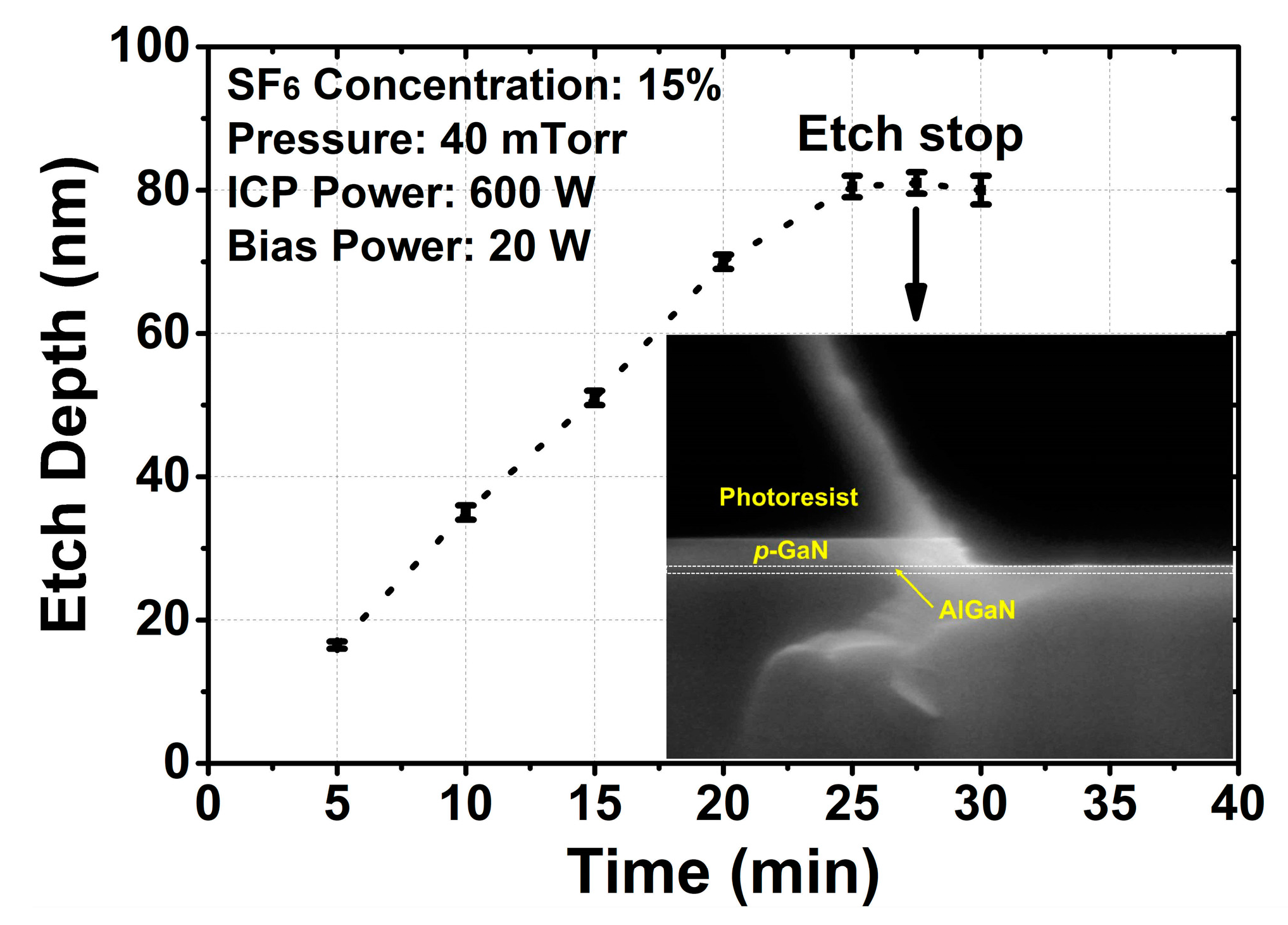
3.1. Etching Parameter Optimization
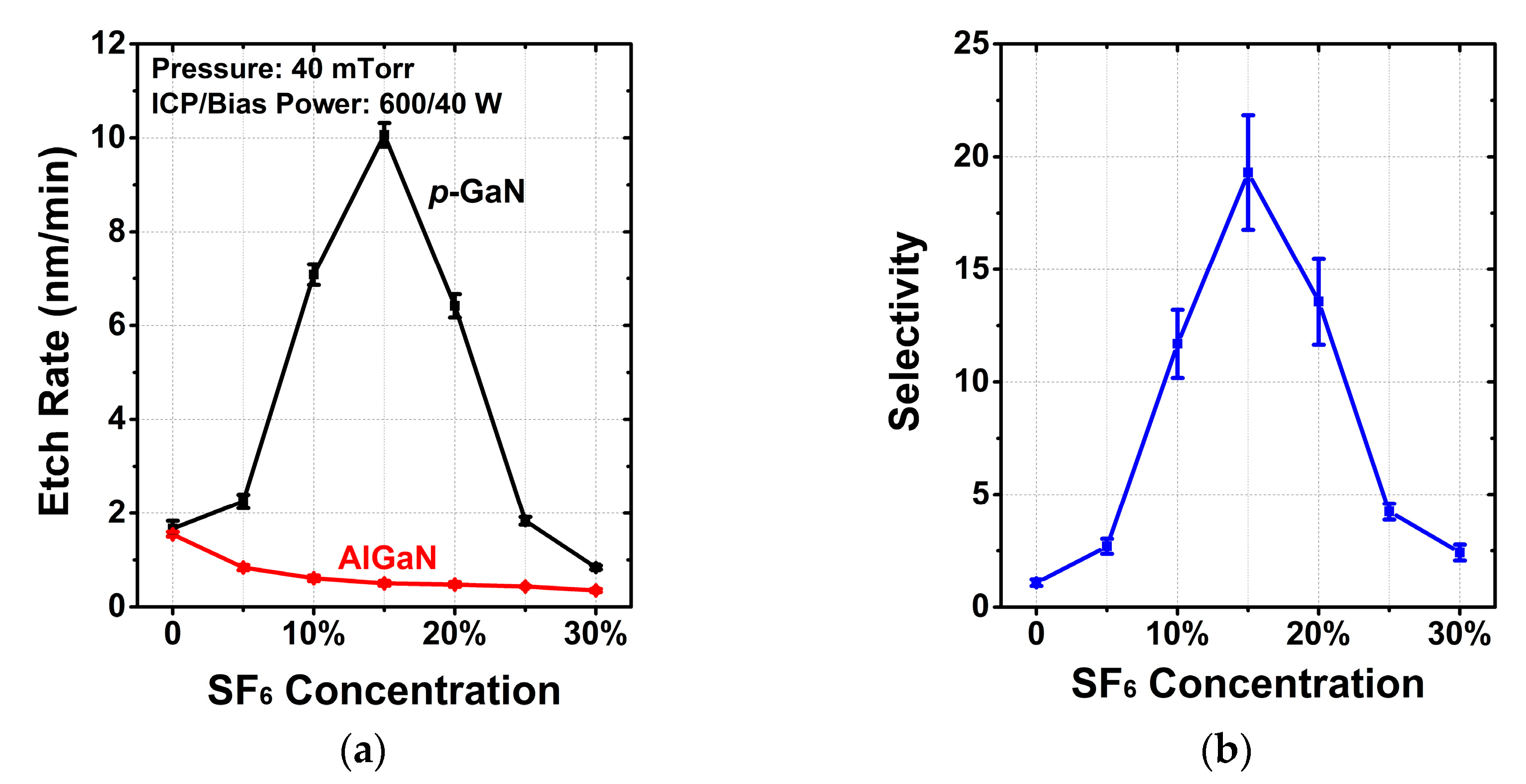
3.1.1. SF6 Concentration
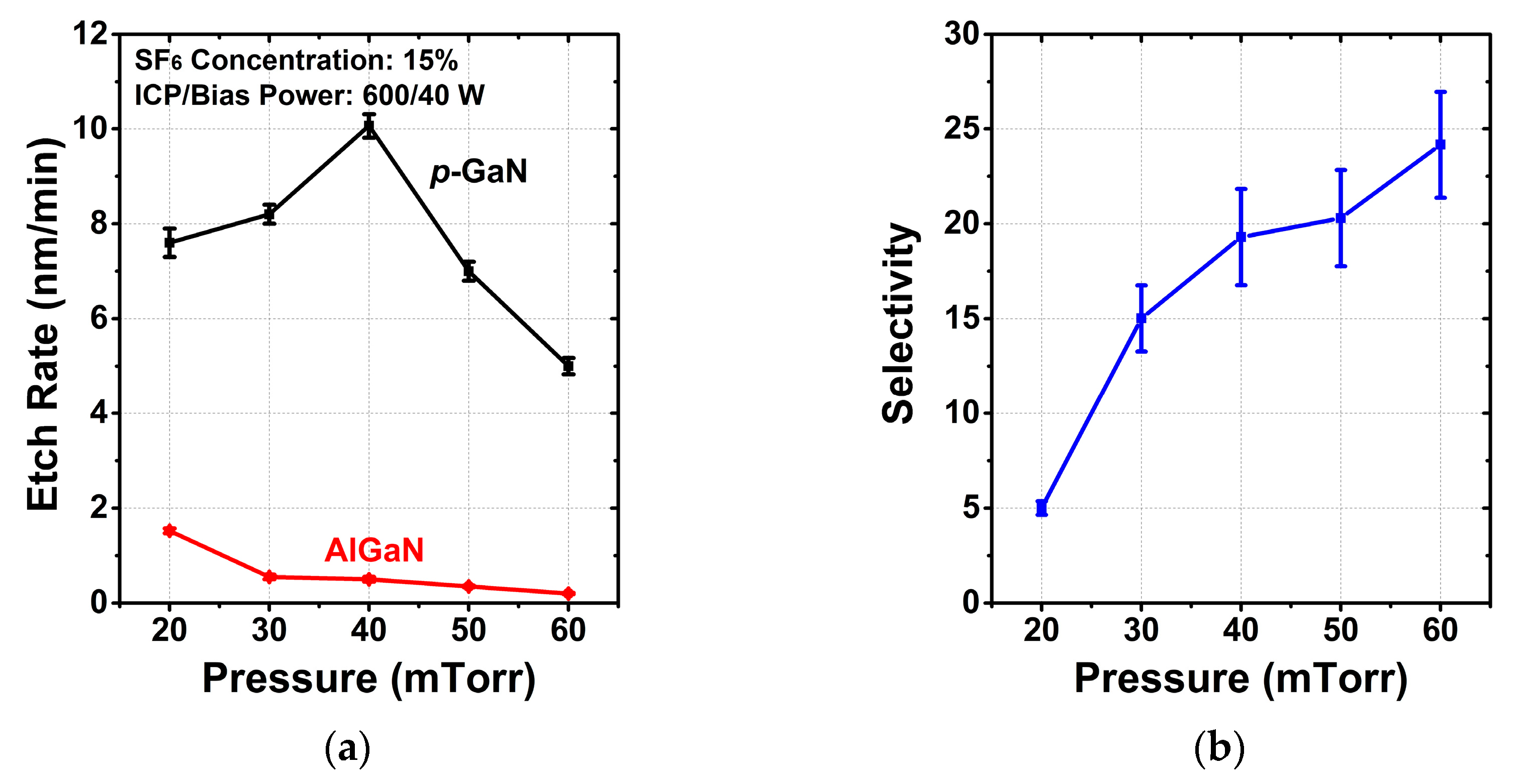
3.1.2. Chamber Pressure
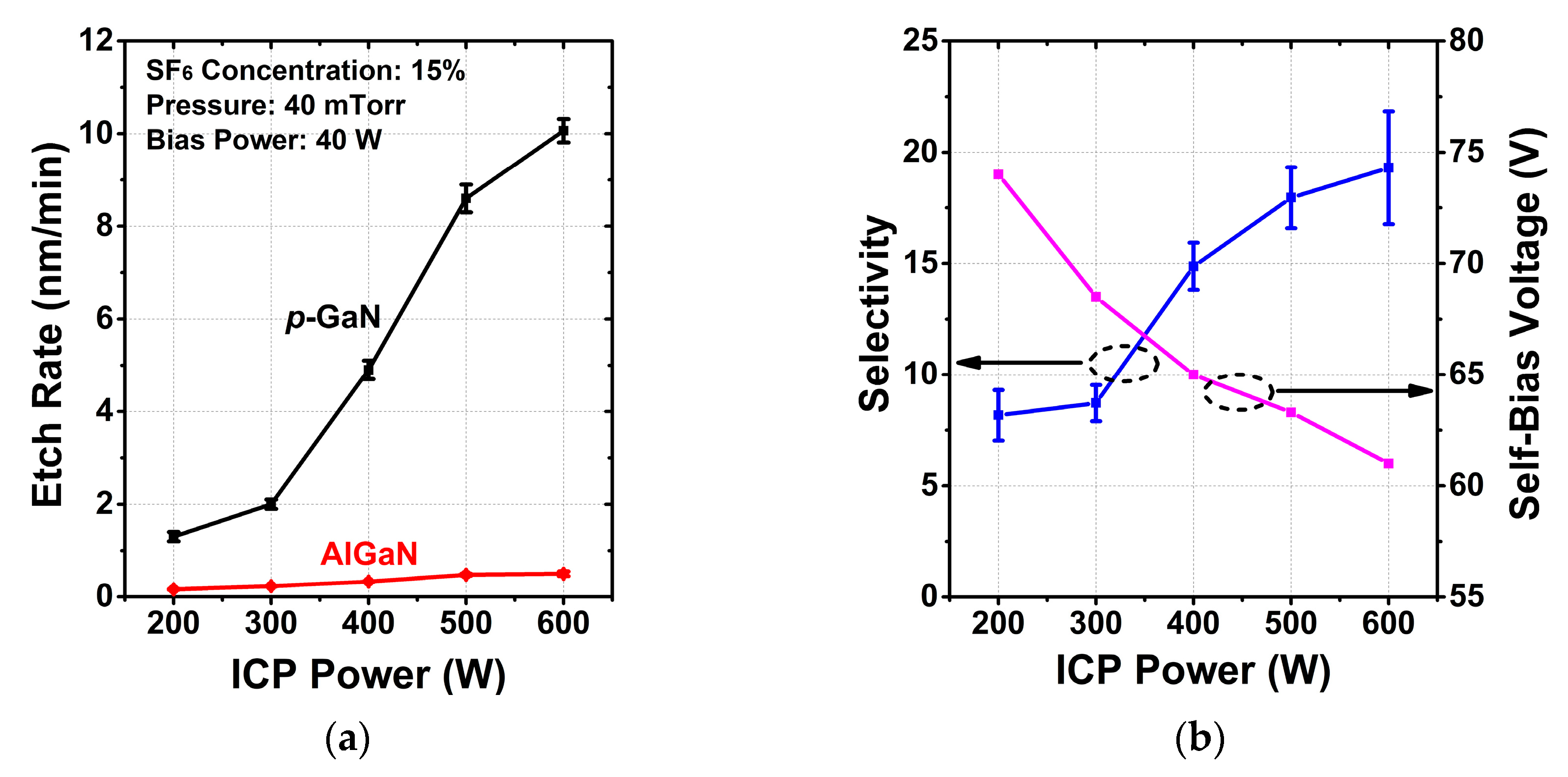
3.1.3. ICP Power
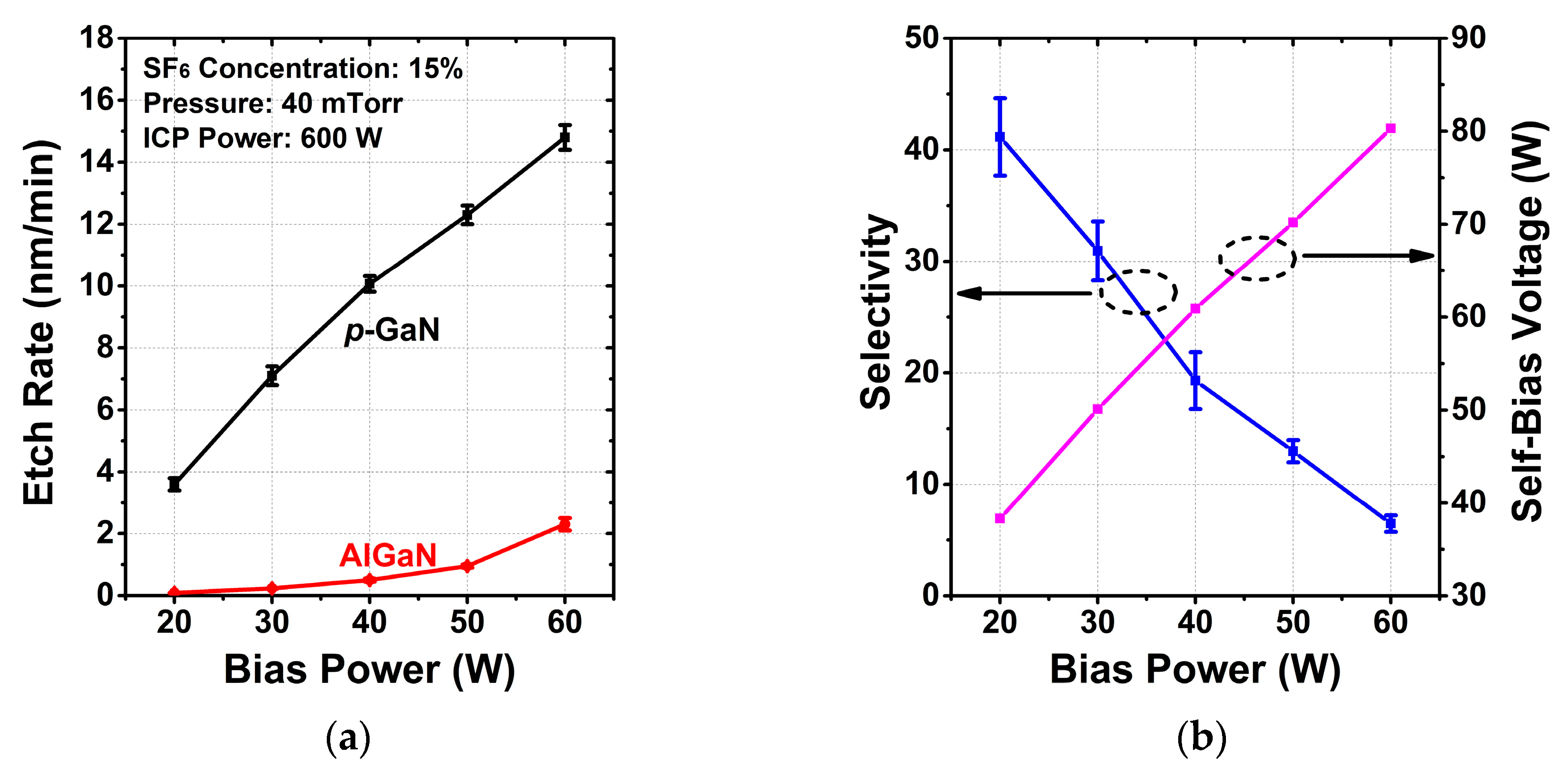
3.1.4. Bias Power
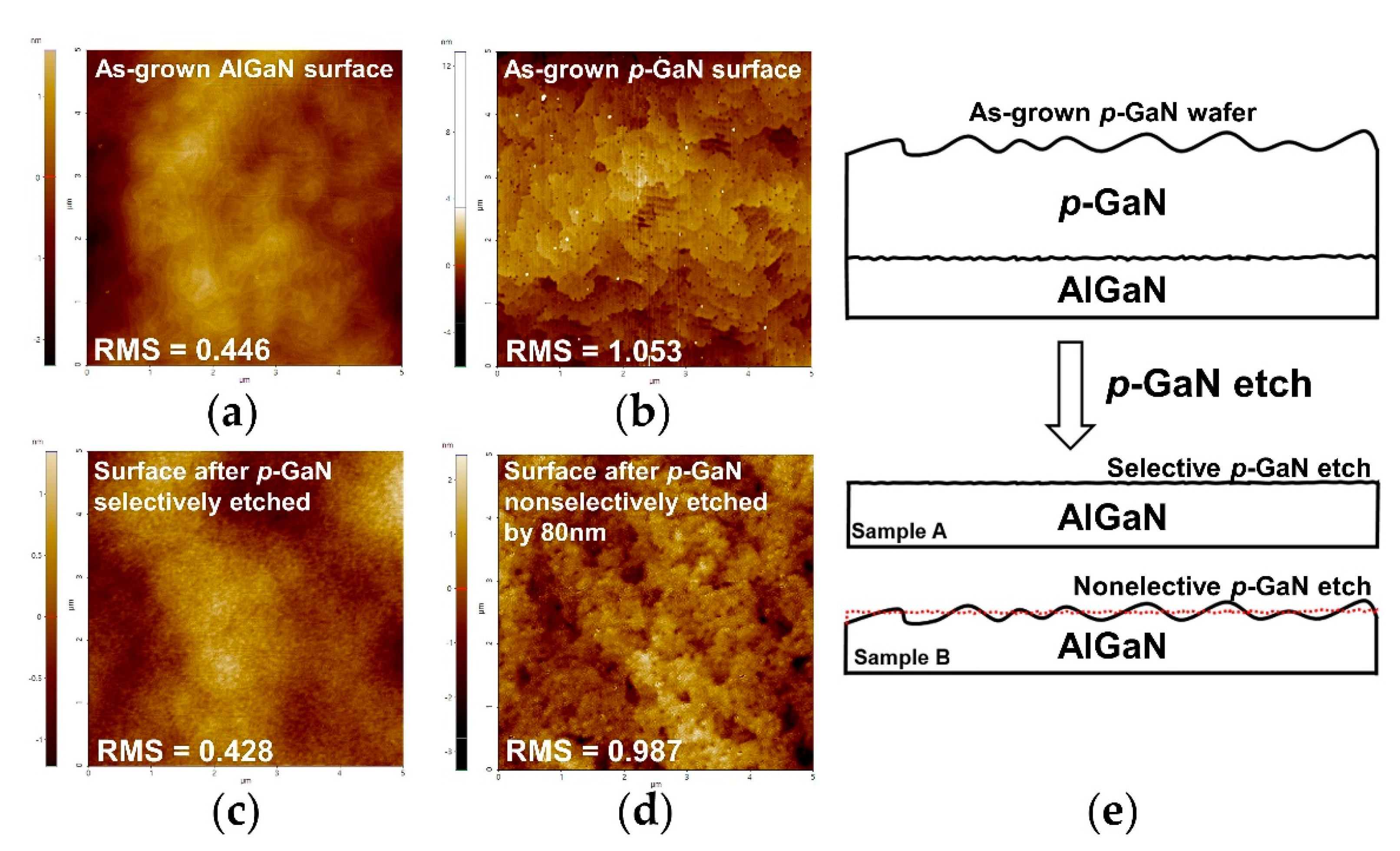
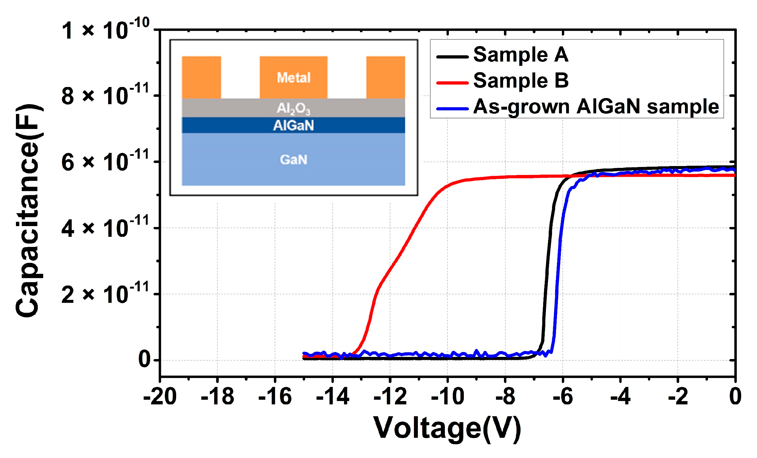
3.2. Etched Surface and Plasma Damage Analysis
4. Conclusions
Author Contributions
Funding
Data Availability Statement
Conflicts of Interest
References
- Ishida, M.; Ueda, T.; Tanaka, T.; Ueda, D. GaN on Si Technologies for Power Switching Devices. IEEE Trans. Electron Devices 2013, 60, 3053–3059. [Google Scholar] [CrossRef] [Scilit]
- Marcon, D.; Saripalli, Y.N.; Decoutere, S. 200mm GaN-on-Si epitaxy and e-mode device technology. In Proceedings of the Electron Devices Meeting, Washington, DC, USA, 5–9 December 2015. [Google Scholar] [CrossRef] [Scilit]
- Sacconi, F.; Carlo, A.D.; Lugli, P.; Morkoc, H. Spontaneous and piezoelectric polarization effects on the output characteristics of AlGaN/GaN heterojunction modulation doped FETs. IEEE Trans. Electron Devices 2001, 48, 450–457. [Google Scholar] [CrossRef]
- Chen, K.J.; Zhou, C. Enhancement-mode AlGaN/GaN HEMT and MIS-HEMT technology. Phys. Status Solidi 2011, 208, 434–438. [Google Scholar] [CrossRef] [Scilit]
- Scott, M.J.; Fu, L.; Zhang, X.; Li, J.; Yao, C.; Sievers, M.; Wang, J. Merits of gallium nitride based power conversion. Semicond. Sci. Technol. 2013, 28, 74013. [Google Scholar] [CrossRef] [Scilit]
- Cai, Y.; Zhou, Y.; Chen, K.J.; Lau, K.M. High-performance enhancement-mode AlGaN/GaN HEMTs using fluoride-based plasma treatment. IEEE Electron Device Lett. 2005, 26, 435–437. [Google Scholar] [CrossRef] [Scilit]
- Saito, W.; Takada, Y.; Kuraguchi, M.; Tsuda, K.; Omura, I. Recessed-gate structure approach toward normally off high-Voltage AlGaN/GaN HEMT for power electronics applications. IEEE Trans. Electron Devices 2006, 53, 356–362. [Google Scholar] [CrossRef] [Scilit]
- Uemoto, Y.; Hikita, M.; Ueno, H.; Matsuo, H.; Ishida, H.; Yanagihara, M.; Ueda, T.; Tanaka, T.; Ueda, D. Gate Injection Transistor (GIT)—A Normally-Off AlGaN/GaN Power Transistor Using Conductivity Modulation. IEEE Trans. Electron Devices 2007, 54, 3393–3399. [Google Scholar] [CrossRef] [Scilit]
- Chen, K.J.; Haberlen, O.; Lidow, A.; Tsai, C.l.; Ueda, T.; Uemoto, Y.; Wu, Y. GaN-on-Si Power Technology: Devices and Applications. IEEE Trans. Electron Devices 2017, 64, 779–795. [Google Scholar] [CrossRef] [Scilit]
- Roccaforte, F.; Greco, G.; Fiorenza, P.; Iucolano, F. An Overview of Normally-Off GaN-Based High Electron Mobility Transistors. Materials 2019, 12, 1599. [Google Scholar] [CrossRef] [Scilit] [PubMed]
- Marcon, D.; Hove, M.V.; Jaeger, B.D.; Posthuma, N.; Wellekens, D.; You, S.; Kang, X.; Wu, T.-L.; Willems, M.; Stoffels, S.; et al. Direct Comparison of GaN-Based E-Mode Architectures (Recessed MISHEMT and p-GaN HEMTs) Processed on 200mm GaN-on-Si with Au-Free Technology. In Proceedings of the SPIE-The International Society for Optical Engineering, San Francisco, CA, USA, 13 March 2015. [Google Scholar] [CrossRef] [Scilit]
- Lukens, G.; Hahn, H.; Kalisch, H.; Vescan, A. Self-Aligned Process for Selectively Etched p-GaN-Gated AlGaN/GaN-on-Si HFETs. IEEE Trans. Electron Devices 2018, 65, 3732–3738. [Google Scholar] [CrossRef] [Scilit]
- Su, L.-Y.; Lee, F.; Huang, J.J. Enhancement-Mode GaN-Based High-Electron Mobility Transistors on the Si Substrate With a P-Type GaN Cap Layer. IEEE Trans. Electron Devices 2014, 61, 460–465. [Google Scholar] [CrossRef] [Scilit]
- Greco, G.; Iucolano, F.; Roccaforte, F. Review of technology for normally-off HEMTs with p-GaN gate. Mater. Sci. Semicond. Process. 2018, 78, 96–106. [Google Scholar] [CrossRef] [Scilit]
- Buttari, D.; Chini, A.; Chakraborty, A.; Mccarthy, L.; Xing, H.; Palacios, T.; Shen, L.; Keller, S.; Mishra, U.K. Selective dry etching of GaN over AlGaN in BCl3/SF6 mixtures. In Proceedings of the IEEE Lester Eastman Conference on High Performance Devices, Troy, NY, USA, 4–6 August 2004. [Google Scholar] [CrossRef] [Scilit]
- Buttari, D.; Chini, A.; Palacios, T.; Coffie, R.; Shen, L.; Xing, H.; Heikman, S.; McCarthy, L.; Chakraborty, A.; Keller, S.; et al. Origin of etch delay time in Cl2 dry etching of AlGaN/GaN structures. Appl. Phys. Lett. 2003, 83, 4779–4781. [Google Scholar] [CrossRef] [Scilit]
- Lee, Y.S.; Sia, J.F.; Nordheden, K.J. Mass spectrometric characterization of BCl3/SF6 plasmas. J. Appl. Phys. 2000, 88, 4507–4509. [Google Scholar] [CrossRef] [Scilit]
- Oh, C.S.; Kim, T.H.; Lim, K.Y.; Yang, J.W. GaN etch enhancement in inductively coupled BCl3 plasma with the addition of N2 and SF6 gas. Semicond. Sci. Technol. 2004, 19, 172–175. [Google Scholar] [CrossRef] [Scilit]
- Feng, M.S.; Guo, J.D.; Lu, Y.M.; Chang, E.Y. Materials Chemistry and Physics. Reactive ion etching of GaN with BCl3/SF6 plasmas. Mater. Chem. Phys. 1996, 45, 80–83. [Google Scholar] [CrossRef] [Scilit]
- Beheshti, M.; Westerman, R. Smooth, low rate, selective GaN/AlGaN etch. AIP Adv. 2021, 11, 25237. [Google Scholar] [CrossRef] [Scilit]
- Qian, R.; Cheng, X.; Zheng, L.; Shen, L.; Zhang, D.; Gu, Z.; Yu, Y. Inductively Coupled Plasma Etching of p-GaN Using Different Masks and Etching Gases. Semicond. Technol. 2018, 43, 449–455. [Google Scholar] [CrossRef]


| Reference | [15] | [21] | This Work | [20] |
|---|---|---|---|---|
| Generator (MHz) | 13.56 | 13.56 | 13.56 | 40 |
| SF6% | 20 | 40 | 15 | 40 |
| Pressure (mTorr) | 37.5 | 20 | 40 | 10 |
| ICP power (W) | 200 | 200 | 600 | / |
| Bias power (W) | 30 | 60 | 20 | / |
| GaN etch rate (nm/min) | 12 | 12 | 3.4 | 0.529 |
| AlGaN etch rate (nm/min) | 0.52 | 1.3 | 0.08 | 0.016 |
| Max. selectivity | 23:1 | 9:1 | 41:1 | 33:1 |
Publisher’s Note: MDPI stays neutral with regard to jurisdictional claims in published maps and institutional affiliations. |
© 2022 by the authors. Licensee MDPI, Basel, Switzerland. This article is an open access article distributed under the terms and conditions of the Creative Commons Attribution (CC BY) license (https://creativecommons.org/licenses/by/4.0/).
Share and Cite
Zhang, P.; Wang, L.; Zhu, K.; Yang, Y.; Fan, R.; Pan, M.; Xu, S.; Xu, M.; Wang, C.; Wu, C.; et al. High Selectivity, Low Damage ICP Etching of p-GaN over AlGaN for Normally-off p-GaN HEMTs Application. Micromachines 2022, 13, 589. https://doi.org/10.3390/mi13040589
Zhang P, Wang L, Zhu K, Yang Y, Fan R, Pan M, Xu S, Xu M, Wang C, Wu C, et al. High Selectivity, Low Damage ICP Etching of p-GaN over AlGaN for Normally-off p-GaN HEMTs Application. Micromachines. 2022; 13(4):589. https://doi.org/10.3390/mi13040589
Chicago/Turabian StyleZhang, Penghao, Luyu Wang, Kaiyue Zhu, Yannan Yang, Rong Fan, Maolin Pan, Saisheng Xu, Min Xu, Chen Wang, Chunlei Wu, and et al. 2022. "High Selectivity, Low Damage ICP Etching of p-GaN over AlGaN for Normally-off p-GaN HEMTs Application" Micromachines 13, no. 4: 589. https://doi.org/10.3390/mi13040589
APA StyleZhang, P., Wang, L., Zhu, K., Yang, Y., Fan, R., Pan, M., Xu, S., Xu, M., Wang, C., Wu, C., & Zhang, D. W. (2022). High Selectivity, Low Damage ICP Etching of p-GaN over AlGaN for Normally-off p-GaN HEMTs Application. Micromachines, 13(4), 589. https://doi.org/10.3390/mi13040589