
On-Chip Optical Beam Manipulation with an Electrically Tunable Lithium-Niobate-on-Insulator Metasurface

 ,
, 
Abstract
:1. Introduction
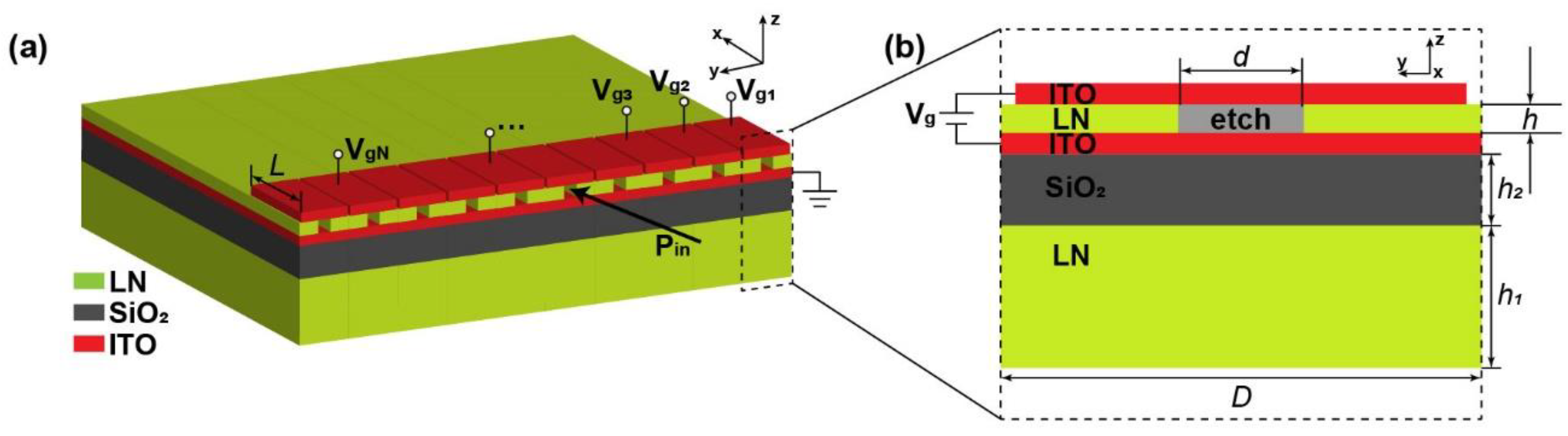
2. Materials and Methods
3. Results
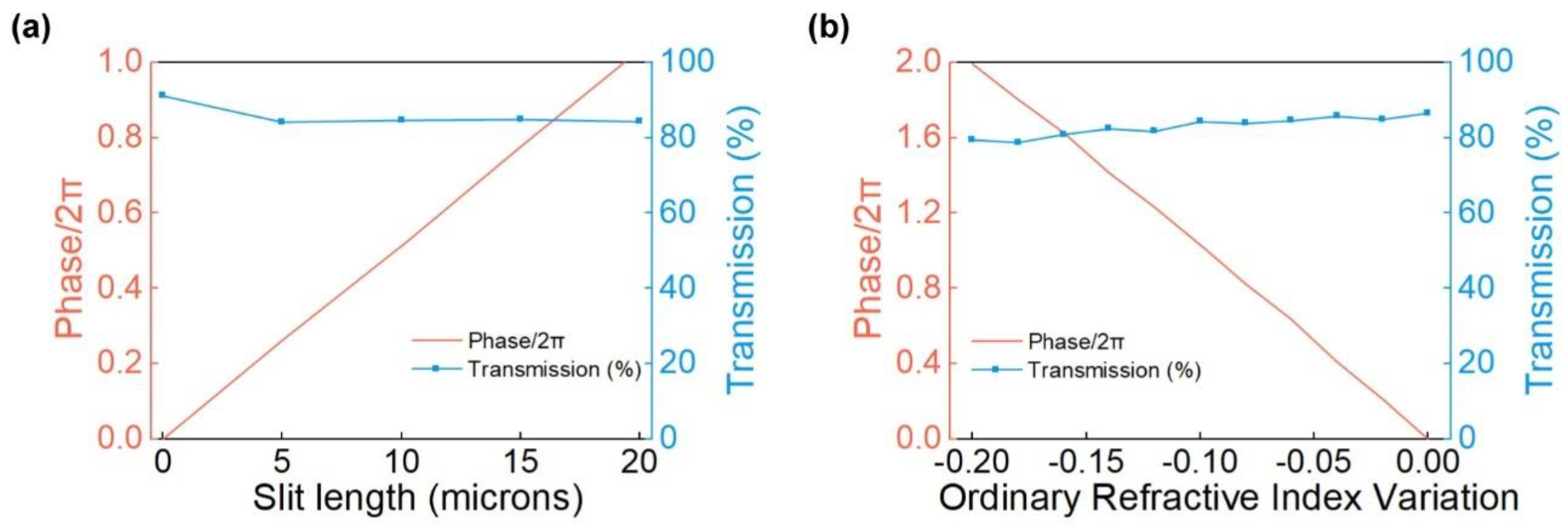
3.1. Units Analysis
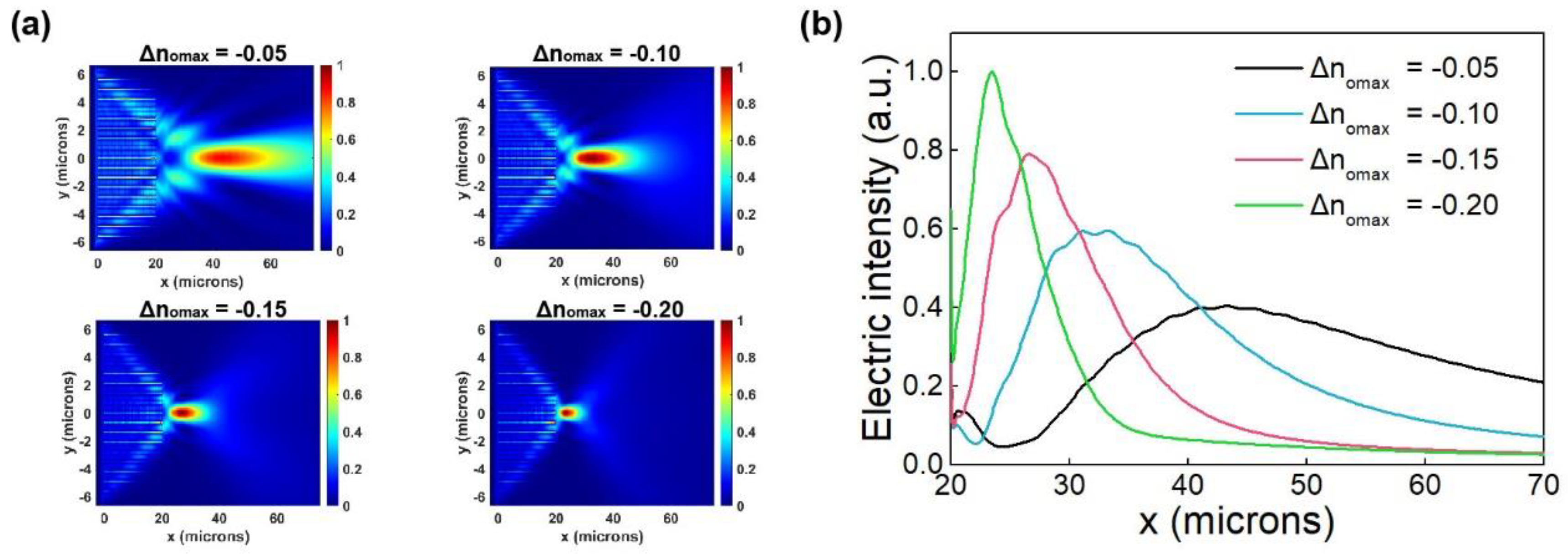
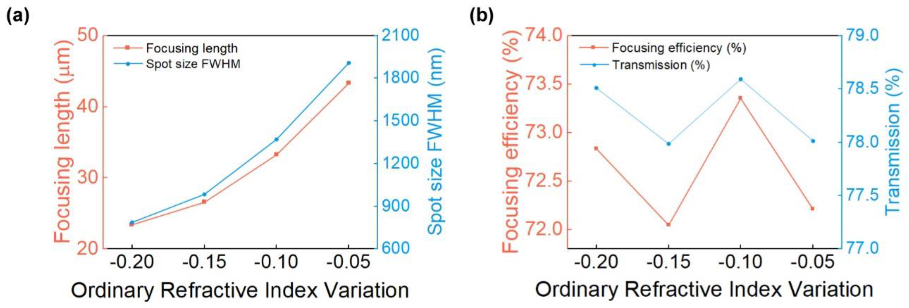
3.2. Focusing Function Design
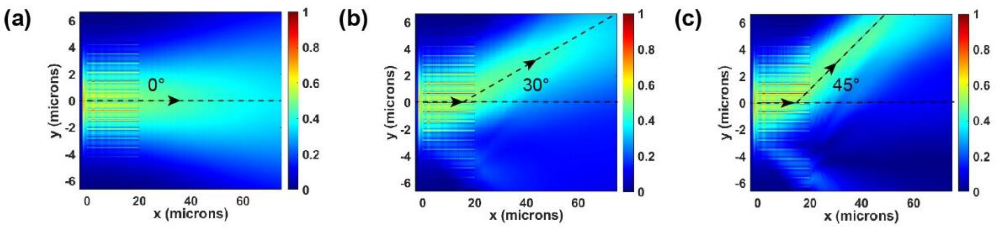
3.3. Deflection Function Design
4. Discussion
Supplementary Materials
Author Contributions
Funding
Institutional Review Board Statement
Informed Consent Statement
Data Availability Statement
Conflicts of Interest
References
- Wang, C.; Zhang, M.; Chen, X.; Bertrand, M.; Shams-Ansari, A.; Chandrasekhar, S.; Winzer, P.; Lončar, M. Integrated lithium niobate electro-optic modulators operating at CMOS-compatible voltages. Nature 2018, 562, 101–104. [Google Scholar] [CrossRef] [PubMed]
- Saravi, S.; Pertsch, T.; Setzpfandt, F. Lithium Niobate on Insulator: An Emerging Platform for Integrated Quantum Photonics. Adv. Opt. Mater. 2021, 9, 2100789. [Google Scholar] [CrossRef]
- Elshaari, A.W.; Pernice, W.; Srinivasan, K.; Benson, O.; Zwiller, V. Hybrid integrated quantum photonic circuits. Nat. Photonics 2020, 14, 285–298. [Google Scholar] [CrossRef]
- Levy, M.; Osgood, R.M.; Liu, R.; Cross, L.E.; Cargill, G.S.; Kumar, A.; Bakhru, H. Fabrication of single-crystal lithium niobate films by crystal ion slicing. Appl. Phys. Lett. 1998, 73, 2293–2295. [Google Scholar] [CrossRef]
- Poberaj, G.; Hu, H.; Sohler, W.; Günter, P. Lithium niobate on insulator (LNOI) for micro-photonic devices. Laser Photonic Rev. 2012, 6, 488–503. [Google Scholar] [CrossRef]
- Qi, Y.; Li, Y. Integrated lithium niobate photonics. Nanophotonics 2020, 9, 1287–1320. [Google Scholar] [CrossRef]
- Takigawa, R.; Higurashi, E.; Kawanishi, T.; Asano, T. Lithium niobate ridged waveguides with smooth vertical sidewalls fabricated by an ultra-precision cutting method. Opt. Express 2014, 22, 27733–27738. [Google Scholar] [CrossRef] [PubMed]
- Guarino, A.; Poberaj, G.; Rezzonico, D.; Degl’Innocenti, R.; Günter, P. Electro–optically tunable microring resonators in lithium niobate. Nat. Photonics 2007, 1, 407–410. [Google Scholar] [CrossRef]
- Zhang, M.; Wang, C.; Cheng, R.; Shams-Ansari, A.; Lončar, M. Monolithic ultra-high-Q lithium niobate microring resonator. Optica 2017, 4, 1536–1537. [Google Scholar] [CrossRef]
- Rabiei, P.; Ma, J.; Chiles, J.; Khan, S.; Fathpour, S. High-QLithium Niobate Microring-Resonators on Silicon. Opt. Soc. Am. 2013, CTu1F-3. [Google Scholar] [CrossRef]
- Wang, C.; Xiong, X.; Andrade, N.; Venkataraman, V.; Ren, X.-F.; Guo, G.-C.; Lončar, M. Second harmonic generation in nano-structured thin-film lithium niobate waveguides. Opt. Express 2017, 25, 6963–6973. [Google Scholar] [CrossRef] [PubMed] [Green Version]
- Chen, P.; Wang, C.; Wei, D.; Hu, Y.; Xu, X.; Li, J.; Wu, D.; Ma, J.; Ji, S.; Zhang, L.; et al. Quasi-phase-matching-division multiplexing holography in a three-dimensional nonlinear photonic crystal. Light Sci. Appl. 2021, 10, 146. [Google Scholar] [CrossRef]
- Wei, D.; Wang, C.; Xu, X.; Wang, H.; Hu, Y.; Chen, P.; Li, J.; Zhu, Y.; Xin, C.; Hu, X.; et al. Efficient nonlinear beam shaping in three-dimensional lithium niobate nonlinear photonic crystals. Nat. Commun. 2019, 10, 4193. [Google Scholar] [CrossRef] [Green Version]
- Wang, C.; Li, Z.; Kim, M.-H.; Xiong, X.; Ren, X.-F.; Guo, G.-C.; Yu, N.; Lončar, M. Metasurface-assisted phase-matching-free second harmonic generation in lithium niobate waveguides. Nat. Commun. 2017, 8, 2098. [Google Scholar] [CrossRef] [PubMed]
- Chen, X.; Meng, Q.; Xu, W.; Zhang, J.; Zhu, Z.; Qin, S. Electrically tunable absorber based on a graphene integrated lithium niobate resonant metasurface. Opt. Express 2021, 29, 32796–32803. [Google Scholar] [CrossRef] [PubMed]
- Hu, Y.; Yu, M.; Zhu, D.; Sinclair, N.; Shams-Ansari, A.; Shao, L.; Holzgrafe, J.; Puma, E.; Zhang, M.; Lončar, M. On-chip electro-optic frequency shifters and beam splitters. Nature 2021, 599, 587–593. [Google Scholar] [CrossRef]
- Cheng, X.; He, T.; Zhou, Z.; Zhang, J.; Jiao, H.; Wang, Z. Multilayer enhanced metasurfaces with high efficiency and additional functionalities. Adv. Opt. Thin Film. VI 2018, 10691, 1069103. [Google Scholar] [CrossRef]
- Cheng, K.; Wei, Z.; Fan, Y.; Zhang, X.; Wu, C.; Li, H. Realizing Broadband Transparency via Manipulating the Hybrid Coupling Modes in Metasurfaces for High-Efficiency Metalens. Adv. Opt. Mater. 2019, 7, 1900016. [Google Scholar] [CrossRef]
- Wei, Z.; Li, H.; Xu, W.; Cao, Y. Dynamic Control of Ultrathin Electromagnetic Absorber Using Active High Impedance Metasurfaces. Front. Phys. 2021, 8, 632902. [Google Scholar] [CrossRef]
- Wei, Z.; Liu, X.; Cao, Y. Switchable Metasurface with Broadband and Highly Efficient Electromagnetic Functionality. Front. Phys. 2020, 8, 90. [Google Scholar] [CrossRef] [Green Version]
- Fan, Y.; Shen, N.-H.; Zhang, F.; Zhao, Q.; Wu, H.; Fu, Q.; Wei, Z.; Li, H.; Soukoulis, C.M. Two-Dimensional Optics: Graphene Plasmonics: A Platform for 2D Optics. Adv. Opt. Mater. 2019, 7, 1970009. [Google Scholar] [CrossRef]
- Fan, Y.; Shen, N.-H.; Zhang, F.; Zhao, Q.; Wu, H.; Fu, Q.; Wei, Z.; Li, H.; Soukoulis, C.M. Graphene Plasmonics: A Platform for 2D Optics. Adv. Opt. Mater. 2019, 7, 1800537. [Google Scholar] [CrossRef] [Green Version]
- Fan, Y.; Tu, L.; Zhang, F.; Fu, Q.; Zhang, Z.; Wei, Z.; Li, H. Broadband Terahertz Absorption in Graphene-Embedded Photonic Crystals. Plasmonics 2018, 13, 1153–1158. [Google Scholar] [CrossRef]
- Fan, Y.; Shen, N.-H.; Zhang, F.; Zhao, Q.; Wei, Z.; Zhang, P.; Dong, J.; Fu, Q.; Li, H.; Soukoulis, C.M. Photoexcited Graphene Metasurfaces: Significantly Enhanced and Tunable Magnetic Resonances. ACS Photonics 2018, 5, 1612–1618. [Google Scholar] [CrossRef]
- Fan, Y.; Shen, N.-H.; Zhang, F.; Wei, Z.; Li, H.; Zhao, Q.; Fu, Q.; Zhang, P.; Koschny, T.; Soukoulis, C.M. Electrically Tunable Goos–Hänchen Effect with Graphene in the Terahertz Regime. Adv. Opt. Mater. 2016, 4, 1824–1828. [Google Scholar] [CrossRef]
- Chen, H.-T.; Taylor, A.J.; Yu, N. A review of metasurfaces: Physics and applications. Rep. Prog. Phys. 2016, 79, 076401. [Google Scholar] [CrossRef] [PubMed] [Green Version]
- Cheng, X.; Zhang, J.; Ding, T.; Wei, Z.; Li, H.; Wang, Z. The effect of an electric field on the thermomechanical damage of nodular defects in dielectric multilayer coatings irradiated by nanosecond laser pulses. Light Sci. Appl. 2013, 2, e80. [Google Scholar] [CrossRef] [Green Version]
- Wei, Z.; Cao, Y.; Su, X.; Gong, Z.; Long, Y.; Li, H. Highly efficient beam steering with a transparent metasurface. Opt. Express 2013, 21, 10739–10745. [Google Scholar] [CrossRef]
- Bukhari, S.S.; Vardaxoglou, J.; Whittow, W. A Metasurfaces Review: Definitions and Applications. Appl. Sci. 2019, 9, 2727. [Google Scholar] [CrossRef] [Green Version]
- Zhang, L.; Mei, S.; Huang, K.; Qiu, C.-W. Advances in Full Control of Electromagnetic Waves with Metasurfaces. Adv. Opt. Mater. 2016, 4, 818–833. [Google Scholar] [CrossRef]
- Wang, Z.; Li, T.; Soman, A.; Mao, D.; Kananen, T.; Gu, T. On-chip wavefront shaping with dielectric metasurface. Nat. Commun. 2019, 10, 3547. [Google Scholar] [CrossRef] [PubMed]
- Ding, P.; Li, Y.; Shao, L.; Tian, X.; Wang, J.; Fan, C. Graphene aperture-based metalens for dynamic focusing of terahertz waves. Opt. Express 2018, 26, 28038–28050. [Google Scholar] [CrossRef] [PubMed]
- Kim, T.-T.; Kim, H.; Kenney, M.; Park, H.S.; Kim, H.-D.; Min, B.; Zhang, S. Amplitude Modulation of Anomalously Refracted Terahertz Waves with Gated-Graphene Metasurfaces. Adv. Opt. Mater. 2018, 6, 1700507. [Google Scholar] [CrossRef]
- Gedney, S. Introduction to the Finite-Difference Time-Domain (FDTD) Method for Electromagnetics. Morgan Claypool 2011, 6, 1–250. [Google Scholar] [CrossRef]
- Zelmon, D.E.; Small, D.L.; Jundt, D. Infrared corrected Sellmeier coefficients for congruently grown lithium niobate and 5 mol.% magnesium oxide–doped lithium niobate. J. Opt. Soc. Am. B 1997, 14, 3319–3322. [Google Scholar] [CrossRef]
- Jazbinšek, M.; Zgonik, M. Material tensor parameters of LiNbO3 relevant for electro- and elasto-optics. Appl. Phys. B 2002, 74, 407–414. [Google Scholar] [CrossRef]
- Zhang, Z.; Qi, X.; Zhang, J.; Guo, C.; Zhu, Z. Graphene-enabled electrically tunability of metalens in the terahertz range. Opt. Express 2020, 28, 28101–28112. [Google Scholar] [CrossRef]
- Chen, X.; Huang, L.; Mühlenbernd, H.; Li, G.; Bai, B.; Tan, Q.; Jin, G.; Qiu, C.-W.; Zhang, S.; Zentgraf, T. Dual-polarity plasmonic metalens for visible light. Nat. Commun. 2012, 3, 1198. [Google Scholar] [CrossRef]
- Bibbò, L.; Khan, K.; Liu, Q.; Lin, M.; Wang, Q.; Ouyang, Z. Tunable narrowband antireflection optical filter with a metasurface. Photonics Res. 2017, 5, 500–506. [Google Scholar] [CrossRef]
- Fan, Z.B.; Qiu, H.Y.; Zhang, H.L.; Pang, X.N.; Zhou, L.D.; Liu, L.; Ren, H.; Wang, Q.H.; Dong, J.W. A broadband achromatic metalens array for integral imaging in the visible. Light Sci. Appl. 2019, 8, 67. [Google Scholar] [CrossRef] [Green Version]
- Gao, Z.; Zhang, C.; Li, H.; Li, Y. Broadband achromatic metalens based on lithium niobite on insulator. J. Phys. D Appl. Phys. 2021, 54, 485103. [Google Scholar] [CrossRef]


| Reference | Wavelength (μm) | Material | F (μm) | FWHM (μm) | Focusing Efficiency | Focusing Length Tunability/μm |
|---|---|---|---|---|---|---|
| [40] | 0.43~0.78 (achromatic) | Si3N4 | 81.5 | 2.5~4.5 | 55% (measurement) | - |
| [41] | 0.4~0.76 (achromatic) | LiNbO3 | 83 | 1.5~3.2 | 71% (simulation) | - |
| [31] | 1.55 | SOI | 25 | 1.07 | 79% (simulation) | - |
| [37] | 30 | Au, Graphene | 161.1~251.5 (tunable) | 48.78~60.62 | 27.15~61.62% (simulation) | 90.4 (~3λ) |
| This work | 1.55 | LNOI | 23.41~43.32 (tunable) | 0.786~1.91 | 72% (simulation) | 19.9 (~13λ) |
Publisher’s Note: MDPI stays neutral with regard to jurisdictional claims in published maps and institutional affiliations. |
© 2022 by the authors. Licensee MDPI, Basel, Switzerland. This article is an open access article distributed under the terms and conditions of the Creative Commons Attribution (CC BY) license (https://creativecommons.org/licenses/by/4.0/).
Share and Cite
Dou, L.; Xie, L.; Wei, Z.; Wang, Z.; Cheng, X. On-Chip Optical Beam Manipulation with an Electrically Tunable Lithium-Niobate-on-Insulator Metasurface. Micromachines 2022, 13, 472. https://doi.org/10.3390/mi13030472
Dou L, Xie L, Wei Z, Wang Z, Cheng X. On-Chip Optical Beam Manipulation with an Electrically Tunable Lithium-Niobate-on-Insulator Metasurface. Micromachines. 2022; 13(3):472. https://doi.org/10.3390/mi13030472
Chicago/Turabian StyleDou, Linyuan, Lingyun Xie, Zeyong Wei, Zhanshan Wang, and Xinbin Cheng. 2022. "On-Chip Optical Beam Manipulation with an Electrically Tunable Lithium-Niobate-on-Insulator Metasurface" Micromachines 13, no. 3: 472. https://doi.org/10.3390/mi13030472
APA StyleDou, L., Xie, L., Wei, Z., Wang, Z., & Cheng, X. (2022). On-Chip Optical Beam Manipulation with an Electrically Tunable Lithium-Niobate-on-Insulator Metasurface. Micromachines, 13(3), 472. https://doi.org/10.3390/mi13030472