Article

Thermal-Resistance Effect of Graphene at High Temperatures in Nanoelectromechanical Temperature Sensors

1
Academy for Advanced Interdisciplinary Research, North University of China, Taiyuan 030051, China
2
State Key Laboratory of Dynamic Measurement Technology, North University of China, Taiyuan 030051, China
3
School of Semiconductors and Physics, North University of China, Taiyuan 030051, China
*
Authors to whom correspondence should be addressed.
Micromachines 2022, 13(12), 2078; https://doi.org/10.3390/mi13122078
Submission received: 2 November 2022 / Revised: 23 November 2022 / Accepted: 24 November 2022 / Published: 26 November 2022
(This article belongs to the Topic MEMS Sensors and Resonators)

Abstract

:
Graphene membranes act as temperature sensors in nanoelectromechanical devices due to their excellent thermal and high-temperature resistance properties. Experimentally, reports on the sensing performance of graphene mainly focus on the temperature interval under 400 K. To explore the sensing performance of graphene temperature sensors at higher temperature intervals, micro-fabricated single-layer graphene on a SiNX substrate is presented as temperature sensors by semiconductor technology and its electrical properties were measured. The results show that the temperature coefficient of the resistance value is 2.07 × 10⁻³ in the temperature range of 300–450 K and 2.39 × 10⁻³ in the temperature range of 450–575 K. From room temperature to high temperature, the “metal” characteristics are presented, and the higher TCR obtained at higher temperature interval is described and analyzed by combining Boltzmann transport equation and thermal expansion theory. These investigations provide further insight into the temperature characteristics of graphene.

1. Introduction

Accurately monitoring temperature with small size has become a critical role not only in life-threatening ailments but also in modern industries with the increasing maturity of micromachining and chip integration technology. Compared with conventional temperature sensors, micro-temperature sensors have attracted research attention because of their miniaturization [1], intelligence [2], and high integration [3,4]. Graphene exhibits excellent properties such as high electron mobility [5], low noise [6], and impressive thermal properties [7,8]. Graphene exhibits the highest thermal conductivity of about 5300 W·m−1·K−1 among the currently known materials [9,10]. Graphene relies on electrons and phonons for heat transfer [11], but the main heat transfer medium is phonons [12]. For this reason, graphene is an ideal material for heat-sensitive elements.
The temperature characteristics of graphene-based sensitive elements such as reduced graphene oxide (rGO) [13,14] and graphene film below 400 K have been reported [15]. However, with the development of technology and the prosperity of industrialization, there is an increasing demand for miniaturized thermal resistance microsensors for high-temperature testing [16,17,18]. For example, in the process of petroleum exploration and development, the measurement of formation temperature, which determines the properties of oil and gas and the way of gas field development, needs to reach above 500 K [18]. In the pharmaceutical process, the monitoring temperature of drug production and sterilization can reach above 530 K [17]. So it is highly necessary to improve the temperature measurement interval of the thermal resistance temperature sensor with high sensitivity. It has been reported that graphene, as an excellent high-temperature resistant material, can maintain stable performance at 973K [19] and exhibits “metallic” characteristics in the temperature range around room temperature because of phonon scattering [20]. However, as a zero-bandgap semi-metallic material, the charge carriers may be excited to participate in the conduction at high temperature, thus, the transition from “gold” to “semiconductor” will occur. To the best of our knowledge, no experimental reports have focused on the temperature characteristics of graphene at high temperatures. Therefore, it is of profound physical significance to explore the scientific question of whether graphene temperature sensors exhibit monotonic properties at high temperatures. In addition, Benyamin Davaji et al. confirmed that the temperature sensor with SiN substrate exhibits the highest temperature coefficient by comparing the sensitivity of micro-fabricated single-layer graphenes (SLGS) on a SiO2/Si substrate, SiN membrane and a suspended architecture [21]. Therefore, a graphene temperature sensor with SiNX/Si substrate to explore the temperature characteristics of graphene in a wider temperature range was fabricated in this study.
In this article, graphene prepared by chemical vapor deposition (CVD) was developed to a thermal resistance nanoelectromechanical graphene temperature sensor by using standard semiconductor processes such as transferring and sputtering. The temperature characteristics of graphene were tested in the temperature range of 300–575 K, and its temperature characteristics were explained by combining Boltzmann theory and thermal expansion theory. Experimental support for the development of temperature sensors with graphene as a sensitive element in a higher range will be provided in this study. Simultaneously, the previously proposed model was improved from the perspective of thermal expansion of the substrate, and the concept that the tensile strain caused by thermal expansion of the substrate intensifies the “metallic” property of graphene was explained. In the temperature interval studied here, the increase of the positive temperature coefficient (PTC) could be described as the superposition of the dominant scattering mechanism of graphene itself and the tensile strain of the external substrate.

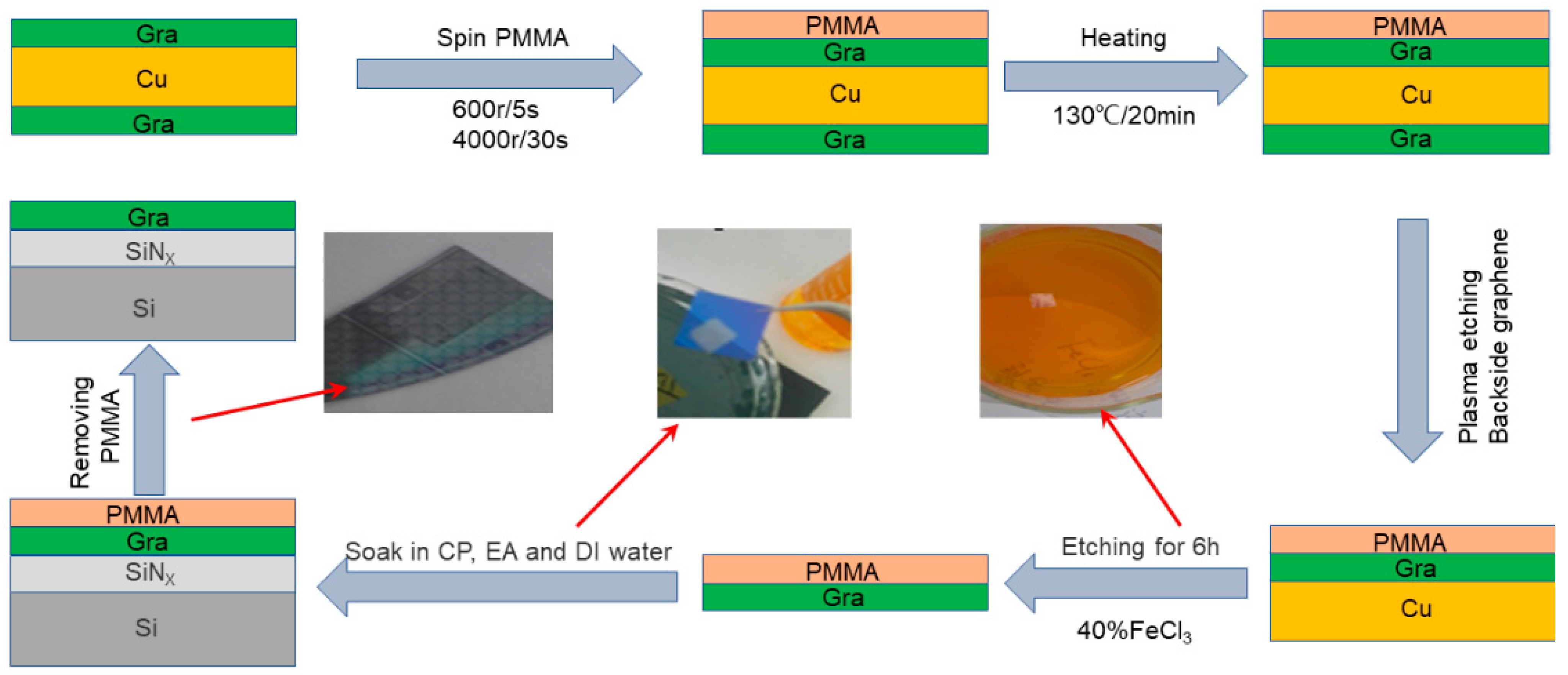
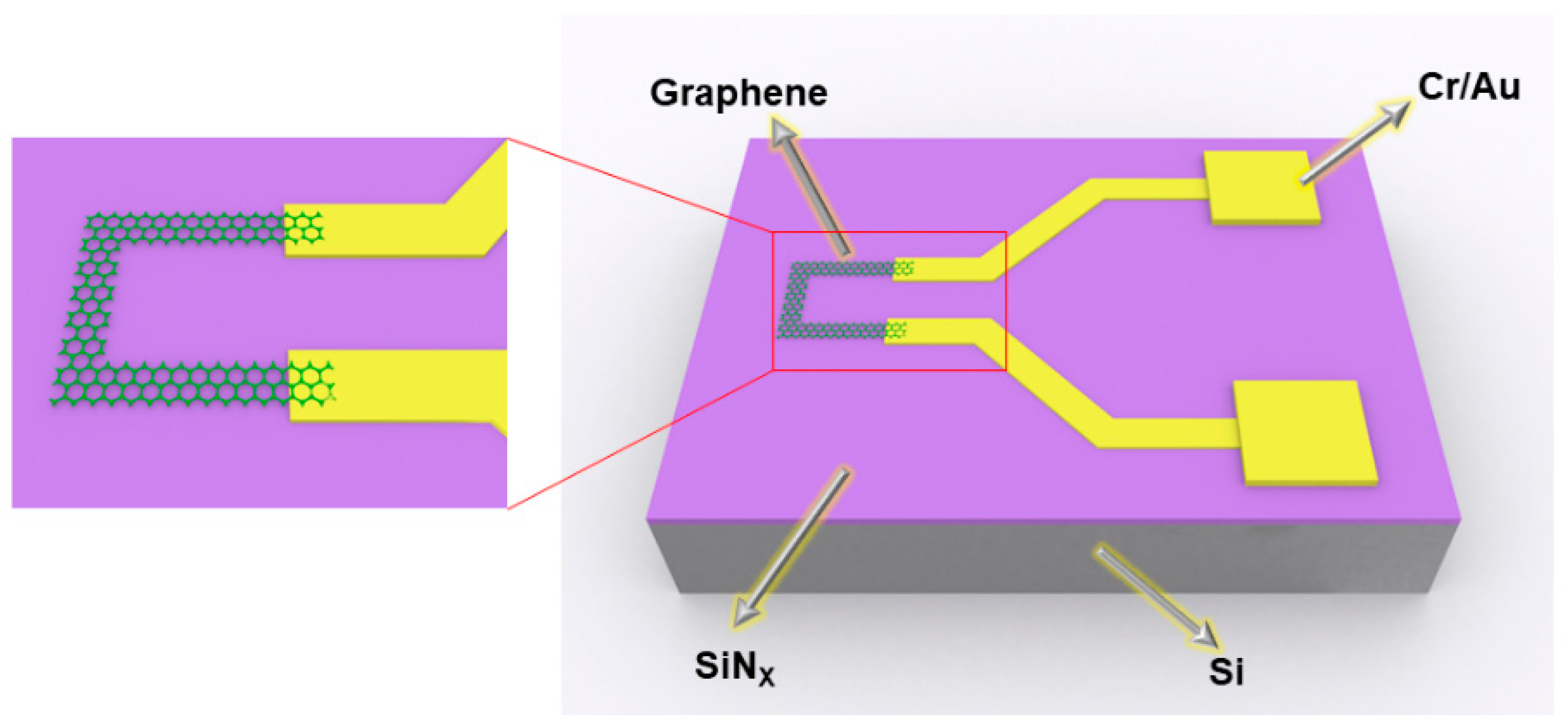
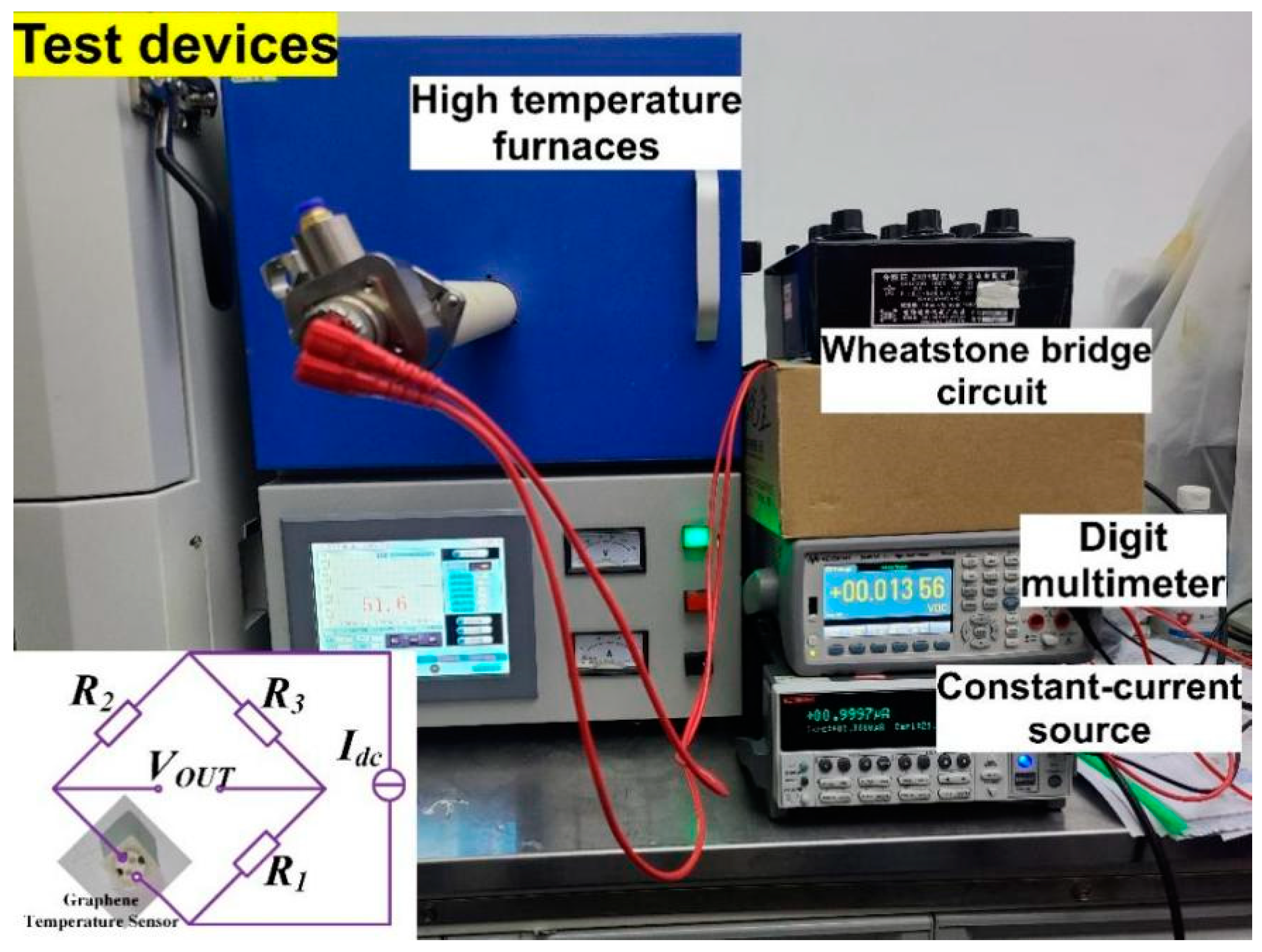
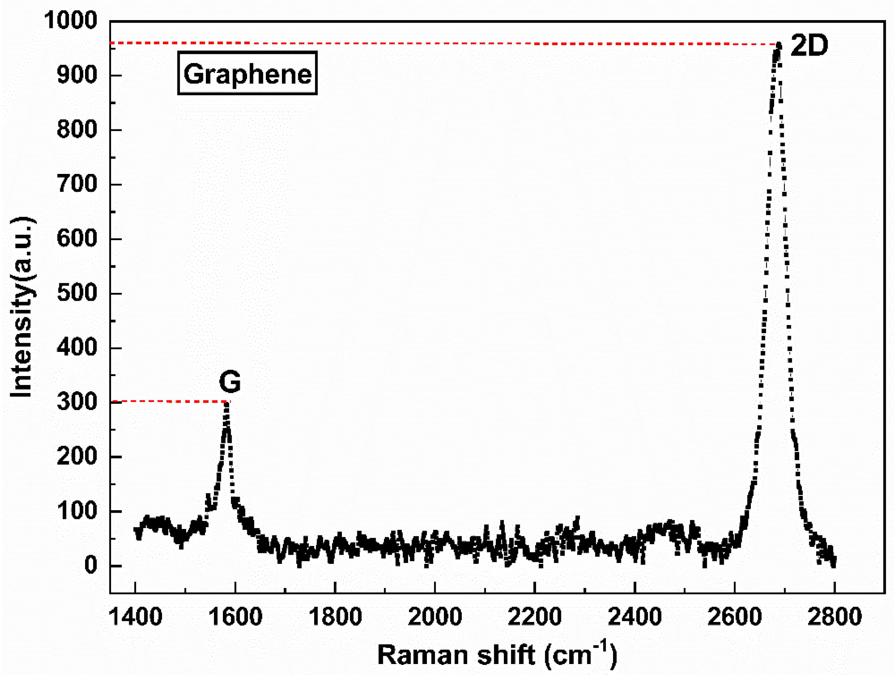
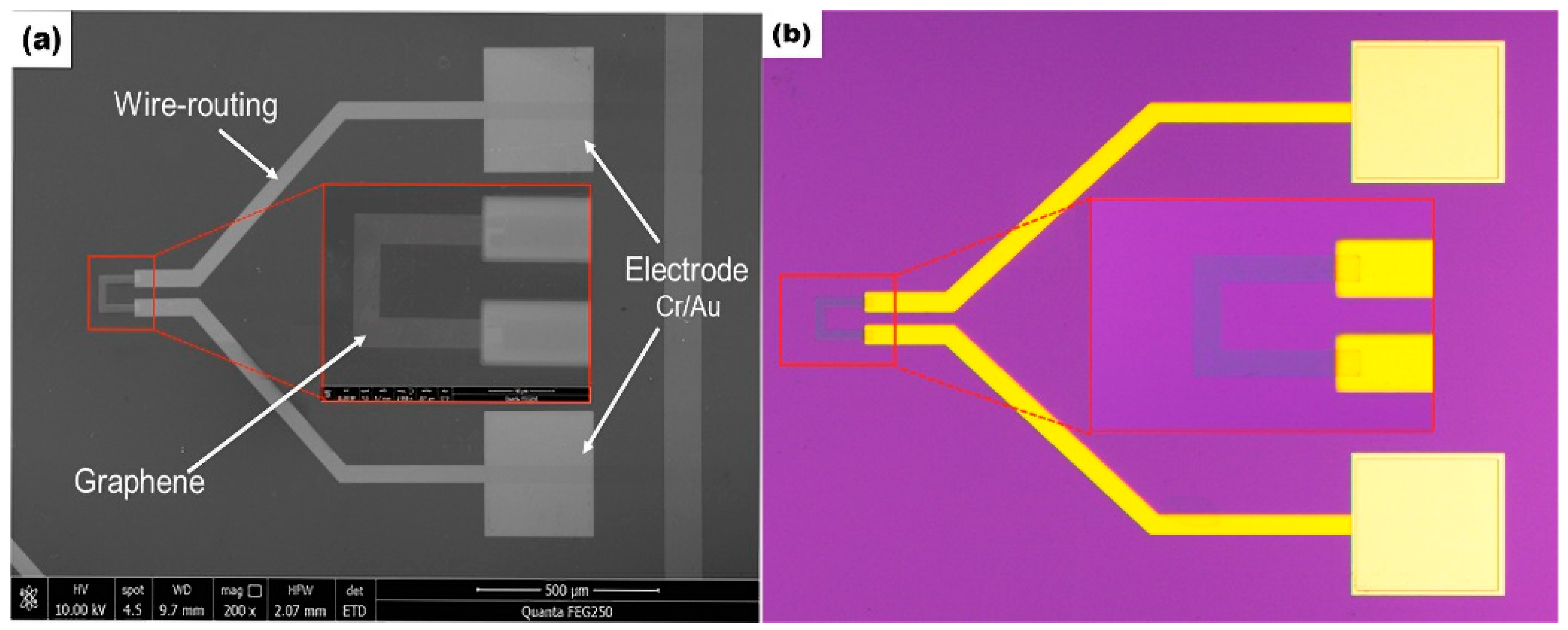
2. Materials and Methods

Graphene was grown on copper substrate by the chemical vapor deposition (CVD) method [22]. A wet transfer method using polymethyl methacrylate (PMMA) as a support layer was used to transfer graphene onto a SiNX/Si substrate (made by plasma-enhanced chemical vapor deposition (PECVD)) pre-deposited with metal electrodes [23,24]. The process of graphene being transferred to the specified substrate is presented in Figure 1. After being cropped into 1.5 × 1.5 cm samples, a spin coater was used to apply graphene to copper foil at speeds of 600 rpm/5 s and 4000 rpm/30 s and performed with polymethyl methacrylate (PMMA). PMMA/Graphene/Cu/Graphene samples were placed on a hot plate at 130 °C for 20 min for hot plate hardening to allow PMMA to bind more tightly to the graphene after curing. Next, the samples were treated with O2 plasma to etch the back graphene of the sample, and 40% FeCl3 was used to etch the Cu substrate supporting the graphene for about 6 h. After that, the PMMA/graphene sample was transferred to the target substrate and heated on a hot plate at 85 °C for 30 min. The PMMA layer was dissolved in acetone (CP) solution at 50 °C for 10 min, and then the target was washed with alcohol (EA) solution and deionized (DI) water. Finally, The graphene was patterned by using lithography and O2 plasma etching. The parameters of O2 plasma etching are as follows: power, 60 W; gas flow, 30 sccm; and etching time 3 min.
The structure of the graphene temperature sensor is shown in Figure 2. 15 nm Cr was deposited as the adhesion layer by UV lithography and magnetron sputtering on the Si/SiNx substrate, and then 25 nm Au was deposited as the bottom electrode, which was connected with the transferred monolayer graphene. The sputtering rate of Cr and Au was 1.26 nm/s and 2.35 nm/s, respectively. The figure on the left is a local magnification of the sensitive unit graphene. The graphene is green, and the connecting wire and electrode are yellow.
After the graphene temperature sensor device was fabricated, the temperature characteristic of the graphene temperature sensor was tested by using a high-temperature sealed tube and a high-temperature furnace combined with a Wheatstone bridge. Figure 3 shows the test diagram of the temperature sensor, where the sensor was placed in a high-temperature sealed tube in a high-temperature furnace. The test temperature was increased from 300 K to 575 K in 25 K increments and was maintained at each temperature for 10 min to stabilize the temperature inside the furnace. In addition, to mitigate the humidity and gas sensitivity effects of the graphene film, the high-temperature furnace was evacuated and repeatedly cleaned with inert nitrogen gas prior to the measurement to ensure its oxygen-free environment.
To accurately measure the change in resistance during the heating process, the device resistance was measured using a Wheatstone bridge (see illustration). The bridge was equilibrated down at room temperature, where R0 was equal to the initial resistance of the sensor at room temperature with a humidity of 45% to 50%. The voltage at both ends of the bridge changed linearly with the change of resistance. The output voltage signal was amplified by an operational amplifier, sampled by a low-pass filter, and finally converted to the corresponding resistance value.

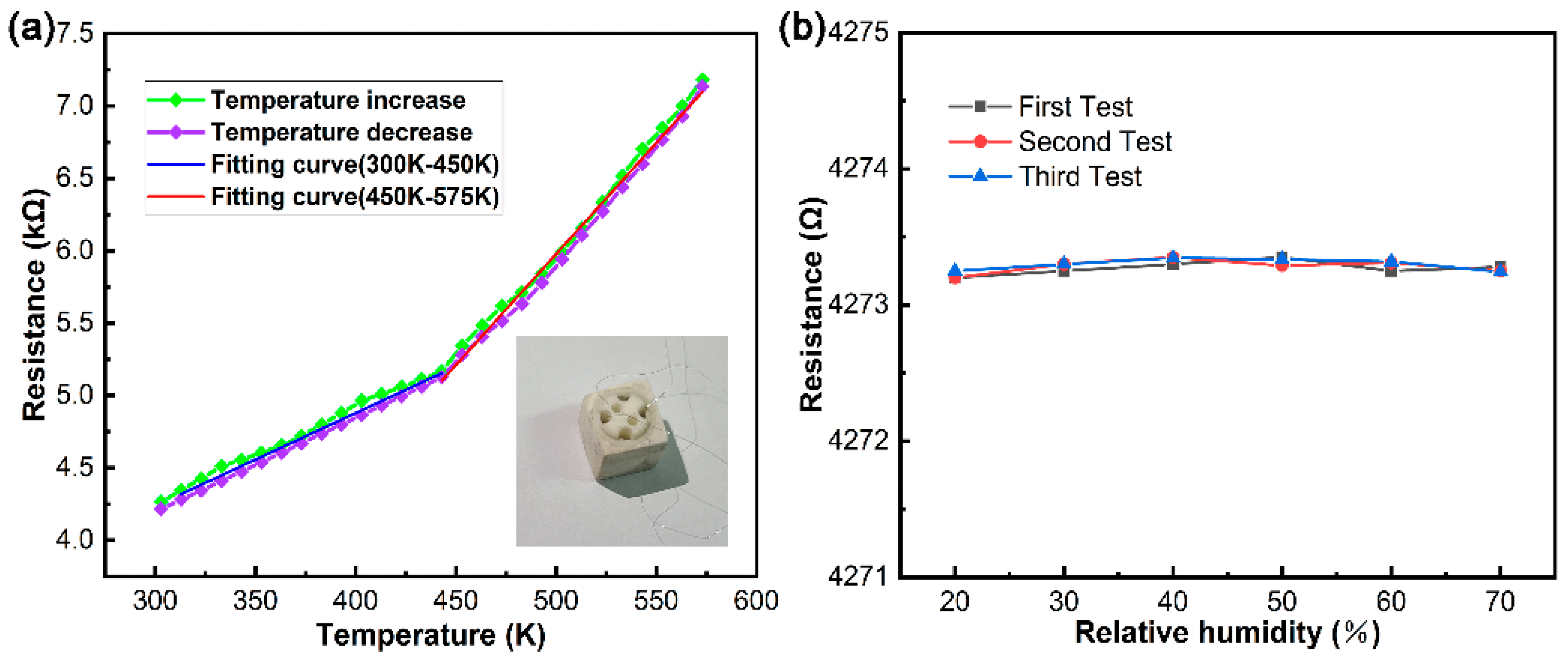
3. Results and Discussion

To characterize the number of layers and defects of graphene after transferring, samples were subjected to Raman scattering (HR-800 Horiba Scientific, Inc., Paris, France) [25]. As shown in Figure 4, the G and 2-D peaks are located at 1582 cm−1 and 2700 cm−1, respectively, and the intensity ratio of the 2-D peak to the G peak (I2D/IG) is 3.21, which indicates that the transferred graphene is a monolayer film [26]. No D peak representing defects appeared at 1350 cm−1, which indicated that the graphene film was of high quality [27], and the defects introduced into graphene during the transferring process could be ignored.
The electrical and thermal conductivity of graphene would be weakened because of the presence of cracks, folds, and organic residues on the graphene surface [28,29,30,31], thus affecting the performance of sensor components. Therefore, to understand the morphology and quality of the graphene surface in the experiment, it was characterized by scanning electron microscopy (Quanta 250, FEI, Inc., Hillsboro, OR, USA) and light microscopy (OM, Axio Scope, Carl Zeiss AG, Oberkochen, Germany). Figure 5a shows the SEM image of the graphene temperature sensor chip, and it can be seen that the transferred graphene surface is smooth and wrinkle-free. Figure 5b shows the chip image of the graphene temperature sensor under the light microscope. From the enlarged area, it can be seen that there is less organic matter residue, no cracks, and a high density of electrode deposition. These results indicated that the transferring quality of graphene films in this experiment was relatively high, and the effect of cracks, folds, and residues on subsequent measurement results could be ignored.
Figure 6a shows the curve of resistance with temperature in the range of 300 to 575 K. The experimental result shows a positive temperature coefficient and the “metal” characteristics because the resistance increases with the increase in temperature, and the resistance decreases with the decrease in temperature. This could be attributed to the dominant phonon scattering in this temperature range, and the enhancement of phonon scattering with the increase in temperature is caused by the decrease in mobility [32,33]. The resistance does not increase linearly with the increase in temperature, which could be attributed to the existence of multiple physical mechanisms in the graphene transport process, such as phonons, screening, Fermi surface effects, and carrier activation, etc., which are all temperature-dependent [34]. Hwang et al. used Boltzmann theory to calculate the relationship between the resistance and temperature of graphene under phonon scattering, which was expressed as ρ ~ T [35], and the resistivity and temperature revealed a linear relationship. Any mechanisms had an impact on the temperature performance of graphene, not only screening that resulted in the “metal” behavior but both the Fermi surface effects and the carrier activation that produced the semiconductor behavior. In the presence of multiple scattering mechanisms, the temperature behavior of graphene depended on the dominant scattering mechanism. Therefore, the relationship between resistance and temperature was not simply summarized as the superposition relationship of multiple scattering mechanisms, ρtol(T) ≠ ρPH(T) +ρother(T). ρtol(T) represented the temperature characteristic that graphene exhibits as resistance varies with temperature. ρPH(T) represented the temperature characteristic exhibited by phonon scattering, and ρother(T) represented all the scattering mechanisms except phonon scattering. This statement explains the non-linear experimental result in the experiment. The humidity test of the device was carried out, and the results are shown in Figure 6b. The results show that the resistance of the encapsulated device is almost not affected by the relative humidity, which indicates that the device can be used normally under different relative humidity environments, and also shows the high reliability of the device.
The temperature coefficient of resistance (TCR) is one of the performance indicators of a temperature sensor. To characterize the performance of the sensor, the TCR can be calculated according to Equation (1). As could be visible in Figure 6, the resistance increased with the increase in temperature, but the slope exhibited an inflection point around 450 K. Therefore, we calculated the TCR in the temperature interval of 300–450 K and 450–475 K, respectively:
T C R = 1 R 0 · R R 0 T T 0
where R0 represents the resistance value at initial temperature T0 and R is the resistance value at temperature T.
The TCR at 300–450 K temperature can be calculated as follows: TCR1 = (5.52425 − 4.2155)/(4.2155·(450 − 300)) = 2.07 × 10⁻³. The TCR at 450–575 K temperature range can be calculated as follows: TCR2 = (7.13572 − 5.52425)/(5.52425·(575 − 450)) = 2.39 × 10⁻³.
After calculation, the TCR of the high-temperature interval is greater than that of the lower-temperature interval. One possible reason is that during the heating process, graphene is subjected to tensile strain from the substrate because SiNX expands with increasing temperature. As a result, the resistance of graphene gradually increases during tensile strain, which indirectly aggravates the “metal” characteristics of graphene, presenting a higher temperature coefficient.
Table 1 shows temperature ranges and TCR for different materials as sensitive junctions are compared. The results show that the graphene temperature sensor has a high-temperature range and high TCR value.

4. Conclusions

A graphene temperature sensor with a temperature range from 300 K to 573 K was fabricated by using standard semiconductor integration technology. Scanning electron microscopy, optical microscopy, Raman analysis revealed that graphene is a single layer of defect-free structure with a clean surface. An electrical performance test using a wheatstone bridge revealed that temperature sensor resistance increased with the increase of temperature, and the reason is that the phonon scattering dominates the presence of the characteristics of “metal” in the temperature range. Simultaneously, the TCR of the high-temperature interval was higher, a possible reason for enhancing this characteristic was explained. In brief, the temperature characteristic of graphene in the range of 300 to 574 K was investigated, and a wide range, good linearity, and high sensitivity graphene temperature sensor has been fabricated, which meets the needs of industrial production and other fields for accurate temperature control at high temperatures.

Author Contributions

Conceptualization, Methodology, Project administration, Writing-original draft. S.L.; Data curation, Investigation, Validation, and Writing-review and editing. N.S.; Funding acquisition, Supervision, M.L. All authors have read and agreed to the published version of the manuscript.

Funding

This research was funded by the “173” Projects of China (Grant No. 2021JCJQJJ0172, 2020JCJQZD043, and 2017JCJQZD006).

Data Availability Statement

Not applicable.

Acknowledgments

The authors would like to appreciate the facility assistance from the Suzhou Institute of Nano-Tech and Nano-Bionics, Chinese Academy of Sciences.

Conflicts of Interest

The authors declare no conflict of interest.

References

  1. Shikida, M.; Hasegawa, Y.; Farisi, M.S.A.; Matsushima, M.; Kawabe, T. Advancements in MEMS technology for medical applications: Microneedles and miniaturized sensors. Jpn. J. Appl. Phys. 2022, 61, SA0803. [Google Scholar] [CrossRef]
  2. Nemec, D.; Janota, A.; Hrubos, M.; Simak, V. Intelligent Real-Time MEMS Sensor Fusion and Calibration. Ieee Sens. J. 2016, 16, 7150–7160. [Google Scholar] [CrossRef] [Green Version]
  3. Li, J. Micro-/Nano-Fiber Sensors and Optical Integration Devices. Sensors 2022, 22, 7673. [Google Scholar] [CrossRef] [PubMed]
  4. Belmonte, J.C.; Puigcorbe, J.; Arbiol, J.; Vila, A.; Morante, J.R.; Sabate, N.; Gracia, I.; Cane, C. High-temperature low-power performing micromachined suspended micro-hotplate for gas sensing applications. Sens. Actuators B-Chem. 2006, 114, 826–835. [Google Scholar] [CrossRef]
  5. Balandin, A.A.; Ghosh, S.; Bao, W.; Calizo, I.; Teweldebrhan, D.; Miao, F.; Lau, C.N. Superior thermal conductivity of single-layer graphene. Nano Lett. 2008, 8, 902–907. [Google Scholar] [CrossRef] [PubMed]
  6. Rumyantsev, S.; Liu, G.; Stillman, W.; Shur, M.; Balandin, A.A. Electrical and noise characteristics of graphene field-effect transistors: Ambient effects, noise sources and physical mechanisms. J. Phys. -Condens. Matter 2010, 22, 395302. [Google Scholar] [CrossRef] [PubMed] [Green Version]
  7. Wang, J.; Mu, X.; Sun, M. The Thermal, Electrical and Thermoelectric Properties of Graphene Nanomaterials. Nanomaterials 2019, 9, 218. [Google Scholar] [CrossRef] [Green Version]
  8. Chu, K.; Wang, X.-h.; Li, Y.-b.; Huang, D.-j.; Geng, Z.-r.; Zhao, X.-l.; Liu, H.; Zhang, H. Thermal properties of graphene/metal composites with aligned graphene. Mater. Des. 2018, 140, 85–94. [Google Scholar] [CrossRef]
  9. Gusynin, V.P.; Sharapov, S.G.; Carbotte, J.P. Unusual microwave response of Dirac quasiparticles in graphene. Phys. Rev. Lett. 2006, 96, 256802. [Google Scholar] [CrossRef] [Green Version]
  10. Wilhelm, M.; Ludwig, T.; Fischer, T.; Yu, W.; Singh, D.; Mathur, S. Functionalized few-layered graphene nanoplatelets for superior thermal management in heat transfer nanofluids. Int. J. Appl. Ceram. Technol. 2022, 19, 803–812. [Google Scholar] [CrossRef]
  11. Laitinen, A.; Kumar, M.; Oksanen, M.; Placais, B.; Virtanen, P.; Hakonen, P. Coupling between electrons and optical phonons in suspended bilayer graphene. Phys. Rev. B 2015, 91, 121414. [Google Scholar] [CrossRef] [Green Version]
  12. Viljas, J.K.; Heikkila, T.T. Electron-phonon heat transfer in monolayer and bilayer graphene. Phys. Rev. B 2010, 81, 245404. [Google Scholar] [CrossRef] [Green Version]
  13. Sehrawat, P.; Islam, A.S.S.; MishraCentre, P. Reduced graphene oxide based temperature sensor: Extraordinary performance governed by lattice dynamics assisted carrier transport. Sens. Actuators B-Chem. 2018, 258, 424–435. [Google Scholar] [CrossRef]
  14. Vasu, K.S.; Chakraborty, B.; Sampath, S.; Sood, A.K. Probing top-gated field effect transistor of reduced graphene oxide monolayer made by dielectrophoresis. Solid State Commun. 2010, 150, 1295–1298. [Google Scholar] [CrossRef] [Green Version]
  15. Kumar, S.; Bhatt, K.; Kumar, P.; Sharma, S.; Kumar, A.; Tripathi, C.C. Laser patterned, high-power graphene paper resistor with dual temperature coefficient of resistance. Rsc Adv. 2019, 9, 8262–8270. [Google Scholar] [CrossRef] [Green Version]
  16. Jiao, P.; Nazar, A.M.; Egbe, K.-J.I.; Barri, K.; Alavi, A.H. Magnetic capsulate triboelectric nanogenerators. Sci. Rep. 2022, 12, 1–10. [Google Scholar] [CrossRef]
  17. Jiang, X.; Kazarin, P.; Sinanis, M.D.; Darwish, A.; Raghunathan, N.; Alexeenko, A.; Peroulis, D. A non-invasive multipoint product temperature measurement for pharmaceutical lyophilization. Sci. Rep. 2022, 12, 1–16. [Google Scholar] [CrossRef]
  18. Macenic, M.; Kurevija, T.; Medved, I. Novel geothermal gradient map of the Croatian part of the Pannonian Basin System based on data interpretation from 154 deep exploration wells. Renew. Sustain. Energy Rev. 2020, 132, 110069. [Google Scholar] [CrossRef]
  19. Gamil, M.; El-Bab, A.M.R.F.; Abd El-Moneim, A.; Nakamura, K. Ultrahigh-sensitivity Graphene-based Strain Gauge Sensor: Fabrication on Si/SiO2 and First-principles Simulation. Sens. Mater. 2018, 30, 2085–2100. [Google Scholar] [CrossRef]
  20. Kaasbjerg, K.; Thygesen, K.S.; Jacobsen, K.W. Unraveling the acoustic electron-phonon interaction in graphene. Phys. Rev. B 2012, 85, 165440. [Google Scholar] [CrossRef]
  21. Davaji, B.; Cho, H.D.; Malakoutian, M.; Lee, J.-K.; Panin, G.; Kang, T.W.; Lee, C.H. A patterned single layer graphene resistance temperature sensor. Sci. Rep. 2017, 7, 1–10. [Google Scholar] [CrossRef]
  22. Kim, S.-M.; Kim, J.-H.; Kim, K.-S.; Hwangbo, Y.; Yoon, J.-H.; Lee, E.-K.; Ryu, J.; Lee, H.-J.; Cho, S.; Lee, S.-M. Synthesis of CVD-graphene on rapidly heated copper foils. Nanoscale 2014, 6, 4728–4734. [Google Scholar] [CrossRef]
  23. Lee, Y.; Bae, S.; Jang, H.; Jang, S.; Zhu, S.-E.; Sim, S.H.; Song, Y.I.; Hong, B.H.; Ahn, J.-H. Wafer-Scale Synthesis and Transfer of Graphene Films. Nano Lett. 2010, 10, 490–493. [Google Scholar] [CrossRef] [Green Version]
  24. Barin, G.B.; Song, Y.; Gimenez, I.d.F.; Souza Filho, A.G.; Barretto, L.S.; Kong, J. Optimized graphene transfer: Influence of polymethylmethacrylate (PMMA) layer concentration and baking time on graphene final performance. Carbon 2015, 84, 82–90. [Google Scholar] [CrossRef]
  25. Ferrari, A.C.; Basko, D.M. Raman spectroscopy as a versatile tool for studying the properties of graphene. Nat. Nanotechnol. 2013, 8, 235–246. [Google Scholar] [CrossRef] [PubMed] [Green Version]
  26. Das, A.; Chakraborty, B.; Sood, A.K. Raman spectroscopy of graphene on different substrates and influence of defects. Bull. Mater. Sci. 2008, 31, 579–584. [Google Scholar] [CrossRef]
  27. Lebioda, M.; Pawlak, R.; Szymanski, W.; Kaczorowski, W.; Jeziorna, A. Laser Patterning a Graphene Layer on a Ceramic Substrate for Sensor Applications. Sensors 2020, 20, 2134. [Google Scholar] [CrossRef]
  28. Pettes, M.T.; Jo, I.; Yao, Z.; Shi, L. Influence of Polymeric Residue on the Thermal Conductivity of Suspended Bilayer Graphene. Nano Lett. 2011, 11, 1195–1200. [Google Scholar] [CrossRef] [PubMed]
  29. Vasic, B.; Zurutuza, A.; Gajic, R. Spatial variation of wear and electrical properties across wrinkles in chemical vapour deposition graphene. Carbon 2016, 102, 304–310. [Google Scholar] [CrossRef]
  30. Chen, S.; Li, Q.; Zhang, Q.; Qu, Y.; Ji, H.; Ruoff, R.S.; Cai, W. Thermal conductivity measurements of suspended graphene with and without wrinkles by micro-Raman mapping. Nanotechnology 2012, 23, 365701. [Google Scholar] [CrossRef]
  31. Lu, Q.; Gao, W.; Huang, R. Atomistic simulation and continuum modeling of graphene nanoribbons under uniaxial tension. Model. Simul. Mater. Sci. Eng. 2011, 19, 054006. [Google Scholar] [CrossRef] [Green Version]
  32. Bolotin, K.I.; Sikes, K.J.; Hone, J.; Stormer, H.L.; Kim, P. Temperature-dependent transport in suspended graphene. Phys. Rev. Lett. 2008, 101, 096802. [Google Scholar] [CrossRef] [PubMed] [Green Version]
  33. Hwang, E.H.; Das Sarma, S. Acoustic phonon scattering limited carrier mobility in two-dimensional extrinsic graphene. Phys. Rev. B 2008, 77, 115449. [Google Scholar] [CrossRef] [Green Version]
  34. Heo, J.; Chung, H.J.; Lee, S.-H.; Yang, H.; Seo, D.H.; Shin, J.K.; Chung, U.I.; Seo, S.; Hwang, E.H.; Das Sarma, S. Nonmonotonic temperature dependent transport in graphene grown by chemical vapor deposition. Phys. Rev. B 2011, 84, 035421. [Google Scholar] [CrossRef] [Green Version]
  35. Das Sarma, S.; Hwang, E.H. Density-dependent electrical conductivity in suspended graphene: Approaching the Dirac point in transport. Phys. Rev. B 2013, 87, 035415. [Google Scholar] [CrossRef] [Green Version]
  36. Wang, C.; Xia, K.; Zhang, M.; Jian, M.; Zhang, Y. An All-Silk-Derived Dual-Mode E-skin for Simultaneous Temperature-Pressure Detection. Acs Appl. Mater. Interfaces 2017, 9, 39484–39492. [Google Scholar] [CrossRef]
  37. Chen, S.; Jiang, K.; Lou, Z.; Chen, D.; Shen, G. Recent Developments in Graphene-Based Tactile Sensors and E-Skins. Adv. Mater. Technol. 2018, 3, 1700248. [Google Scholar] [CrossRef]
  38. Kim, Y.-J.; Le, T.-S.D.; Nam, H.K.; Yang, D.; Kim, B. Wood-based flexible graphene thermistor with an ultra-high sensitivity enabled by ultraviolet femtosecond laser pulses. Cirp Ann. -Manuf. Technol. 2021, 70, 443–446. [Google Scholar] [CrossRef]
  39. Kula, P.; Szymanski, W.; Kolodziejczyk, L.; Atraszkiewicz, R.; Dybowski, K.; Grabarczyk, J.; Pietrasik, R.; Niedzielski, P.; Kaczmarek, L.; Clapa, M. High Strength Metallurgical Graphene—Mechanisms of Growth and Properties. Arch. Metall. Mater. 2015, 60, 2535–2541. [Google Scholar] [CrossRef]
Figure 1. Schematic diagram of graphene transferring process.
Micromachines 13 02078 g001
Figure 2. The structure diagram of the graphene temperature sensor.
Micromachines 13 02078 g002
Figure 3. Field test diagram.
Micromachines 13 02078 g003
Figure 4. Raman spectra of graphene.
Micromachines 13 02078 g004
Figure 5. (a) SEM image of the chip. (b) Optical microscope image of the chip.
Micromachines 13 02078 g005
Figure 6. (a) The resistance of the temperature sensor as a function of temperature. (b) Humidity characteristics of the device.
Micromachines 13 02078 g006
Table 1. Comparison of different materials’ temperature characteristics.
MaterialsTemperature (K)TCR (K−1)
Silicon rubber-CB, CNTs [36]293–3530.00572
PVDF-MWCNTs, PEN [37]295–3730.081
RGO [14]303–343−1.7 × 10⁻³
Graphene ink [15]213–333−1.55 × 10⁻³ to −1.02 × 10⁻³
Laser-induced-graphene [38]294–3540.573 × 10−3
Metallurgical graphene [39]6–360−1.5 × 10⁻⁴
Graphene (CVD) [This work]300–5732.39 × 10−3
Publisher’s Note: MDPI stays neutral with regard to jurisdictional claims in published maps and institutional affiliations.

