Abstract
Monocrystalline silicon is an important material for processing electronic and photovoltaic devices. The fixed diamond wire sawing technology is the first key technology for monocrystalline silicon wafer processing. A systematic study of the relationship between the fracture strength, stress and breakage rate is the basis for thinning silicon wafers. The external vibration excitation of sawing machine and diamond wire lead to the transverse vibration and longitudinal vibration for silicon wafers. The transverse vibration is the main reason of wafer breakage. In this paper, a mathematical model for calculating breakage ratio of silicon wafer is established. The maximum stress and breakage ratio for as-sawn silicon wafers are studied. It is found that the maximum amplitude of the silicon wafers with the size of 156 mm × 156 mm × 0.2 mm was 160 μm during the diamond wire sawing process. The amplitude, maximum stress and breakage rate of the wafers increased with the increase of the cutting depth. The smaller the silicon wafer thickness, the larger of silicon wafer breakage ratio. In the sawing stage, the breakage ratio of the 156 mm × 156 mm section with a thickness of 0.15 mm of silicon wafers is 6%.
1. Introduction
In the photovoltaic industry, wire sawing technology is the first process of silicon wafer processing. Its processing quality and processing cost affect the total manufacturing cost of the photovoltaic industry [1,2,3,4,5]. At present, more than 95% of silicon wafers are cut by diamond wire saws, and its processing cost accounts for about 15% of the total cost of the photovoltaic industry [6,7,8]. Reducing the thickness of silicon wafer and increasing the yield of silicon wafer are measures to reduce the processing cost [9,10,11,12]. Liu et al. [13] calculated that decreasing wafer thickness from 160 to 50 µm can potentially get a capex reduction of USD 0.14/(W/year) and a cost reduction of USD 0.07/W of the current PV module, which in 2019 had an average price of USD 0.26/W [8].
However, with the decrease of silicon wafer thickness and the development of wire sawing technology towards high-speed direction, the breakage ratio of silicon wafer in wire sawing will increase [14,15,16,17]. Therefore, it is necessary to study the influence of silicon wafer thickness and external factors on the mechanical properties of silicon wafer in the sawing process. The research results of some scholars show that the smaller the wafer thickness of monocrystalline silicon, the worse the mechanical stability, and the easier the crack propagation in the wafer, leading to the increase of wafer breakage ratio [18,19,20,21,22].
The fracture strength and stress state of silicon wafers affect the breakage ratio of wafers [23]. A systematic study of the relationship between the fracture strength, stress and breakage ratio is the basis for determining the thickness of wafers [24,25]. In the cutting process of monocrystalline silicon wafers by using resin bonded diamond wire saw, the wafer stress is related to the wafer vibration station. The wafer vibration state is constantly changing, so the wafer stress is constantly changing too. The vibration of monocrystalline silicon wafer in the sawing process includes transverse vibration and longitudinal vibration, and the transverse vibration is the main reason of wafer breakage [26]. Therefore, this chapter mainly studies the transverse vibration of slice and analyzes the maximum stress of slice caused by transverse vibration. The relationship between fracture strength, stress and fragmentation rate was established to determine the slice thickness under a certain fragmentation rate. From now on, there is no relevant report on the research of breakage ratio of silicon wafer during diamond wire sawing.
Hence, a theoretical model is established in order to solve the above problems. The free vibration and forced vibration of silicon wafers are studied based on the theory of elastic thin plate. Breakage ratio of wafers is analyzed by using the Weibull distribution theory. The research results are of great significance for reducing the thickness and breakage rate of silicon wafers and increasing the yield of silicon wafers.
2. Model of Wafer Breakage during Diamond Wire Sawing
2.1. Free Vibration of Wafer during Wire Sawing
During fixed diamond wire sawing, the wire periodically moves back and forth to cut the silicon ingot. Diamond abrasives scratch the material and generate cutting force on the silicon wafer. Cutting force, the flow of cutting fluid and machine vibration all have effect on the wafer vibration. The silicon ingot is adhered on the connection plate by using the resin glue. The lateral vibration and tangential vibration are generated under the influence of external excitation. In these two vibrations, the lateral vibration is considered as the major reason of causing wafer break because of a larger stress is generated in the lateral vibration. The thickness of as-sawn silicon wafer for photovoltaic industry is 0.2 mm, which is far less than the length 156 mm. Furthermore, one side of silicon wafer is a fixed side, and the other side is free. Thus, the silicon wafer can be seen as a cantilever plate. Therefore, the silicon wafer is treated as the elastic cantilever plate in this paper. The process of diamond wire sawing silicon ingot is shown in Figure 1.
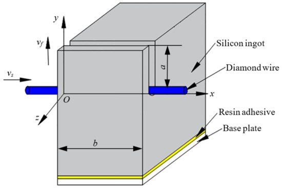
Figure 1.
The process of diamond wire sawing.
One coordinate system is established for diamond wire sawing. The origin point is located as the entry point of diamond wire. The axial direction of diamond wire is the x direction, and the opposite direction of feed direction is the y direction, as shown in Figure 1. The length of silicon wafer is 156 mm, and this parameter is denoted as b. The cutting depth of silicon ingot a is from 0~156 mm. The thickness variation of wafers is ignored to simplified calculation model.
The vibration equation for the sliced silicon wafer is obtained based on the thin plate theory:
where w is the amplitude of sliced silicon wafer; D is the flexural rigidity of wafer, which is related to the elastic modulus E, wafer thickness h and Poisson’s ratio μ, . Ρ is the density of silicon.
The boundary conditions for cantilever plate are:
- (1)
- fixed boundary (geometric boundary condition
- (2)
- free boundary
The method of separation of variables is used to solve the Equation (1) based on the thin plate theory. According to this method, the vibration equation can be written as:
where the W (x,y) is the shape function; ω is the natural frequency of vibration; φ0 is the initial phase.
The integral-transform method is used to simplify the fourth-order differential equation in order to obtain the shape function. This method transforms the high-order differential equation to a simple system of linear equations. The solution of Equation (1) can be obtained by solving the linear equations with the integral-transform method. The shape function W (x,y) after transformation is:
In Equation (7), the coefficients Cmn, Rmn, Tmn, αm, and βn can be obtained separately by the following formulas:
Combining the shape function (7) and the boundary condition Equations (2)–(5), the following equations can be obtained:
The unknown variables in Equation (11) are Im, Jm, Kn and Ln. The condition of Equation (11) has non-zero solution is that the matrix determinant describing the coefficient of the system of linear equations is equal to zero. The natural frequency of silicon wafer is obtained by setting the matrix determinant equal to zero. After that, the four variables can be solved. The four variables Im, Jm, Kn, Ln are the coefficients about four sides of half sine series and bending moment of cosine series according to thin plate theory. Thus, setting Im = −Jm and Im = Jm can yield the symmetrical mode and anti-symmetrical mode respectively. Therefore, the Equations (6) and (7) can be known.
2.2. Forced Vibration of Wafer during Wire Sawing
- (1)
- Force analysis for silicon wafer
During diamond wire sawing, diamond abrasives scratch on silicon ingot under the drive of wire movement. Each grain generates impact force on the wafer within a certain time. Force induced by each grain can be seen as an impact force which value is ∆F and action time is ∆t. Thus, the total cutting force is equal to the sum of each action force induced by every grain. The impact force is assumed as an impulse excitation as shown in Figure 2, which value is ∆F and action time is ∆t. The action time is concerned with the wire speed vs. silicon ingot length L, that is:
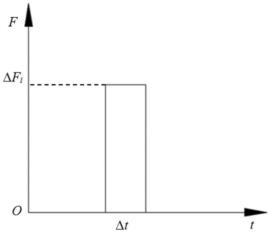
Figure 2.
Impulse excitation induced by single grain.
A lot of diamond abrasives take part in cutting, that means the total cutting force is equal to the sum of each value of impulse excitation at a moment. Because of the shape, diameter and protrusion height for each diamond grain are all different, the cutting depth is various. Hence, the total cutting force changes with shift of time. When the sawing process reaches a steady state, the sawing force is a stationary random fluctuation external excitation. To simplify the cutting process, the total cutting force is simplified as a harmonic force.
which ωf is the frequency of cutting force.
Normal cutting force and tangential force are generated during diamond wire sawing. The normal force distributes along the axial direction of diamond wire, which has no effect on the lateral vibration of silicon wafer and not be considered. Hence, the normal force is vertical to the surface of kerf, and this force can be decomposed into two kinds of force, perpendicular silicon wafer surface Fz and parallel to wafer surface respectively Fy, as shown in Figure 3. The force Fz has the effect on the lateral vibration of silicon wafer. Therefore, the effect of Fz is only consider in the following calculation.
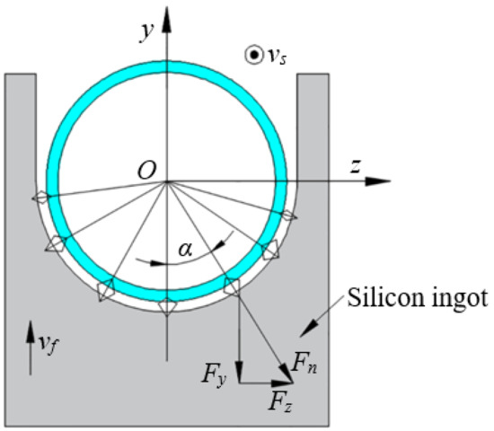
Figure 3.
Force analysis for silicon wafer.
According to reference [27], the total normal cutting force for diamond wire sawing is:
where vf is the feed rate; vs is the wire speed; d is the diameter of the diamond wire; and L is the length of the silicon ingot.
By combining the above three equations, the force Fz can be obtained as follows:
Then in the x direction, the total transverse load FZ is:
Suppose that the sawing force is a harmonic force, the frequency is ωF, and the initial phase is φF:
The distributed load q (x,y,t) can be expressed as:
where R is the radius of diamond wire.
The transverse load FP on silicon wafer during sawing is:
- (2)
- Forced vibration of silicon wafer
Cutting force applied to the silicon wafer induces wafer vibration, which is a forced vibration problem. The dynamic response of silicon wafer can be obtained based on the thin plate theory:
where Wmn, Ttmn are vibration mode obtained by Equation (7) and component of vibration mode respectively. Combining Equation (1), the forced vibration equation is:
On the basis of orthogonality between vibration modes, the following equation is satisfied:
Combining Equations (22) and (23), the following formula is obtained:
The above equation can be transformed another form about Ttmn by using orthogonality of vibration modes:
where FPmn (t) is generalized force for (m,n) vibration mode; and Mmn is generalized mass for (m,n) vibration mode. These two variables can be obtained from the Formulas (26) and (27):
The solution for the Equation (25) can be obtained based on the vibration theory of single degree of freedom system:
and these variables can be obtained by Formulas (29)–(32).
Combing Equations (21) and (28), the vibration response of silicon wafer is:
The Duhamel integral for the harmonic force is:
Hence, the vibration response of silicon wafer can be rewritten as:
It is assumed that the initial displacement w0 and velocity for silicon wafer are all zero. Therefore, the amn and bmn are all zero based on the Equations (29) and (30). Thus, Equation (35) can be simplified as:
Hence, the vibration response of silicon wafer can be rewritten as:
2.3. Stress in Silicon Wafer
The stress applied to silicon wafer is obtained based on the Kirchhoff plate theory. The stress σz parallel to the neutral surface of silicon wafer is neglected as a secondary cause. Aside from that, the shear deformation induced by shear stress τyz and τxz are ignored as well. The other three stress σx, σy and τxy distribute linearly along wafer thickness, which can be obtained by the following equation if the vibration of wafer has been known:
The principal stress for an arbitrary point in the wafer is:
Thus, the maximum principal stress for an arbitrary point in the silicon wafer is obtained, which is used to calculate the breakage ratio of wafers.
2.4. Breakage Ratio for Wafer during Wire Sawing
Stress and machining damage are the major factors influencing wafer breakage. Machining damage such as micro crack, residual stress, dislocation and slip are inevitable during diamond wire sawing, which have different effects on the wafer strength. Lots of researchers have been studied the influence of machining damage on sawn wafer strength. Their experimental results are used for as sawn silicon wafer in this part. The principal stress for an arbitrary point in the silicon wafer is compared to obtain the maximum principal stress which is used to calculate the wafer breakage ratio.
Based on the probabilistic fracture mechanics, the break probability for wafers is:
where σmax is the maximum applied stress in silicon wafer; σ0 is scale parameter of Weibull distribution; mA is the shape parameter of Weibull distribution. From the reference [28], these two Weibull parameters are taken 151.3 Mpa and 3.5.
3. Results and Discussion
The breakage ratio of sawn silicon wafers during diamond wire sawing can be obtained by using the established model. The used parameter values are shown in Table 1.

Table 1.
Parameter values used in calculation.
Each order nature frequency of silicon wafer is solved by Equations (8)–(11) for different cutting depth. After that, vibration shape function is obtained using Equation (7) through solving the four unknown parameters Im, Jm, Kn and Ln. Then the vibration response of wafer, stress and breakage ratio can be solved gradually by using the established theoretical model.
3.1. Free Vibration
The first fourth modes of nature frequency are calculated for sawn wafer when cutting depth is 156 mm, and the FEM simulation is adopted to get the natural frequency in order to verify the correctness of the established model. The results obtained by these two methods are shown in Table 2. It can be seen that, the results are comparable, which indicates the correctness of this established model.
Table 2.
Natural frequency obtained by theoretical model and FE.
The symmetrical mode and anti-symmetrical mode vibration are obtained by setting Im = −Jm and Im = Jm respectively, as shown in Figure 4.
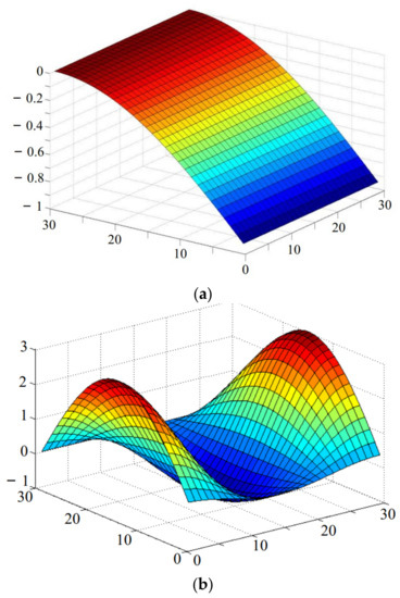
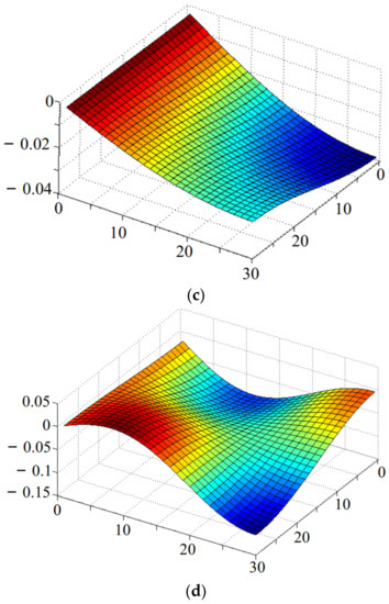
Figure 4.
Vibration mode of free vibration for sawn silicon wafer. (a) First order of symmetrical mode. (b) Second order of symmetrical mode. (c) First order of anti-symmetrical. (d) Second order of anti-symmetrical.
3.2. Forced Vibration and Stress in Silicon Wafer
The amplitude of the wafer is the superposition of each vibration order. Since the natural frequency of the silicon wafer increases with the increase of the order, the amplitude caused by the vibration of the higher order is very small. Therefore, the transverse vibration of silicon wafer is mainly generated by the superposition of lower order vibration. The maximum amplitude is recorded with the changes of cutting depth. The vibration sate of the point (b/2, a) is shown in Figure 5 when the cutting depth is 156 mm. It can be seen the maximum vibration amplitude is about 160 μm when wire speed is 2 m/s and feed rate is 6 μm/s. The excitation frequency is 50 Hz, thus the amplitude of force vibration at the edge point (b/2, a) of the silicon wafer, so the amplitude variation period at this point is also 50 Hz.
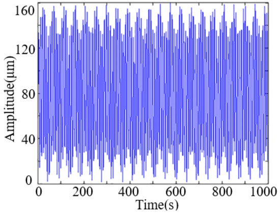
Figure 5.
Vibration state of point (b/2, a) when cutting depth is 156 mm.
Different cutting depths lead to the maximum vibration amplitude is different, the results are shown in Figure 6. The maximum vibration amplitude becomes larger with the increase of cutting depth. In addition, the maximum vibration amplitudes for different thickness silicon wafers are compared. The variation tendency of maximum amplitude for these three kinds of sawn silicon wafer is similar. The thinner of silicon wafer, the larger vibration amplitude.
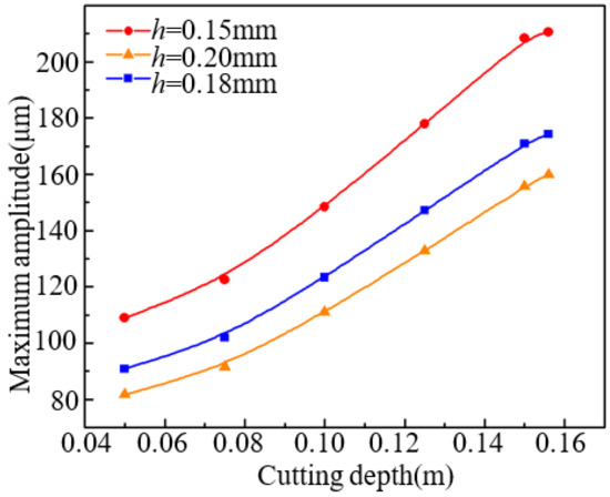
Figure 6.
Changes of maximum amplitude for three kinds of as-sawn wafers.
Larger vibration amplitude leads to larger maximum stress for silicon wafer as shown in Figure 7. Because of the distance between free side and fixed side is larger with increase of cutting depth, the maximum stress increase gradually as well. The variation trend of maximum stress is accord with the changes of maximum vibration amplitude. At the initial stage of diamond wire sawing, the maximum stress changes gently. While at the end of diamond wire sawing, the maximum stress increases sharply. This kind of change of maximum stress accords with the changes of maximum amplitude. Moreover, it indicates that the end stage of diamond wire sawing is difficult to handle because of larger maximum stress. If the adhesive strength between wafer and basal plate is not larger enough, the wafer may drop out and generate waste wafer.
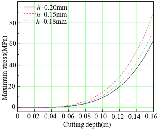
Figure 7.
Changes of maximum stress with cutting depth for three kinds of wafer.
3.3. Breakage Ratio for As-Sawn Silicon Wafer
Take the same cutting parameters as above, the results of breakage ratio with the increase of cutting depth for silicon wafers with different thickness are shown in Figure 8. It can be seen that, the breakage ratio is very small and changes relatively little when the cutting depth is less than 0.1 m. While the breakage ratio increases sharply when the cutting depth is larger than 0.125 m for these three kinds of silicon wafer. The trend of wafer breakage ratio is accord with the changes of vibration amplitude and maximum stress.
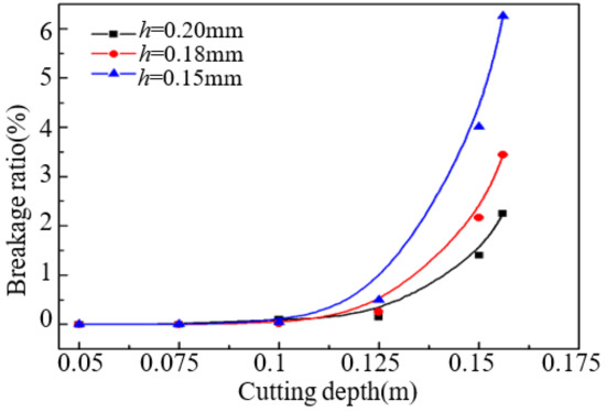
Figure 8.
Changes of breakage ratio with cutting depth for three kinds of wafer.
During calculate the breakage ratio for silicon wafer, the same machining damage on the three kind of silicon wafer is assumed. It means the Weibull parameters for Weibull strength distribution are same. Thus, the breakage ratio is concerned with wafer surface area and stress. From the analysis previous, the maximum stress and surface area become larger with the increase of cutting depth. This leads to the increase of wafer breakage ratio with increase of cutting depth. Furthermore, thinner silicon wafer has larger breakage ratio because of larger maximum stress. When the cutting stage is completed, the breakage ratio for 0.15 mm wafer is about 6%, while that for 0.2 mm wafer is about 2%.
4. Conclusions
In this paper, a mathematical model for calculating breakage ratio of silicon wafer is established based on the fracture mechanism. The maximum stress and breakage ratio for as-sawn silicon wafer are studied. This paper first study the breakage ratio of silicon wafers during diamond wire sawing. The results can be used to optimize processing parameters for diamond wire saw in order to thinning wafer thickness and increasing yield. The main conclusions of this paper are as follows:
- (1)
- The forced vibration model of the wafer during the sawing process was established, and the steady-state solution of the forced vibration of the wafers was obtained. The first five natural frequencies of the wafers were calculated using the finite element and the model of this paper respectively. The maximum relative error of the two methods was 3.43%, indicating the accuracy of the model in this paper.
- (2)
- The maximum amplitude of silicon wafer with the size of 156 mm × 156 mm × 0.2 mm was 160 μm during the diamond sawing process. The amplitude, maximum stress and breakage ratio of wafers increased with the increase of the cutting depth, and the smaller the wafer thickness, the larger the increase.
- (3)
- In the sawing stage, the breakage ratio of the 156 mm × 156 mm section with a thickness of 0.15 mm silicon wafer is 6%.
Author Contributions
T.L. established the theoretical model, analyzed the data, wrote and revised the paper. Y.S. guided the computing program writing. P.G. approved to submit the manuscript. All authors have read and agreed to the published version of the manuscript.
Funding
This paper is supported by National Natural Science Foundation of China (No.51775317, No.52175418), Key Research and Development Program of Shandong Province (No.2019JZZY020209, No.2022CXGC010201) and Shandong Natural Science Foundation (ZR2021ME174).
Conflicts of Interest
We declare that there is no conflict of interest to this work. We declare that we do not have any commercial or associative interest that represents a conflict of interest in connection with the work submitted.
References
- Fraunhofer ISE. Photovoltaics Report; Fraunhofer ISE: Freiburg im Breisgau, Germany, 2020. [Google Scholar]
- Eckhouse, B. Solar and Wind Cheapest Sources of Power in Most of the World; Bloomberg: New York, NY, USA, 2020. [Google Scholar]
- Benayad, A.; Hajjaji, H.; Coustier, F.; Benmansour, M.; Chabli, A. Surface chemical-bonds analysis of silicon particles from diamond-wire cutting of crystalline silicon. J. Appl. Phys. 2016, 120, 235308. [Google Scholar] [CrossRef]
- Wu, H. Wire sawing technology: A state-of-the-art review. Precis. Eng. 2016, 43, 1–9. [Google Scholar] [CrossRef]
- Ge, M.; Wang, P.; Bi, W.; Ge, P. Fabrication of thin resin-bonded diamond wire and its application to ductile mode wire sawing of mono-crystalline silicon. Mater. Sci. Semicond. Process. 2021, 126, 105665. [Google Scholar] [CrossRef]
- VDMA. International Technology Roadmap for Photovoltaic (ITRPV), 11th ed.; VDMA: Frankfurt, Germany, 2020. [Google Scholar]
- Louwen, A.; Sark, W.V.; Schropp, R.; Faaij, A. A cost roadmap for silicon heterojunction solar cells. Sol. Energy Mater. Sol. Cells 2016, 147, 295–314. [Google Scholar] [CrossRef]
- Bellanger, P.; Slaoui, A.; Roques, S.; Ulyashin, A.G.; Debucquoy, M.; Straboni, A.; Sow, A.; Salinesi, Y.; Costa, I.; Serra, J.M. Silicon foil solar cells on low cost supports. J. Renew. Sustain. Energy 2018, 10, 023502. [Google Scholar] [CrossRef]
- Liu, J.; Yao, Y.; Xiao, S.; Gu, X. Review of status developments of high-efficiency crystalline silicon solar cells. J. Phys. D: Appl. Phys. 2018, 51, 123001. [Google Scholar] [CrossRef]
- Ballif, C.; Haug, F.J.; Boccard, M.; Verlinden, P.J.; Hahn, G. Status and perspectives of crystalline silicon photovoltaics in research and industry. Nat. Rev. Mater. 2022, 7, 597–616. [Google Scholar] [CrossRef]
- Dong, Z.; Lin, Y. Ultra-thin wafer technology and applications: A review. Mater. Sci. Semicond. Process. 2020, 105, 104681. [Google Scholar] [CrossRef]
- Abadie, K.; Montméat, P.; Enot, T.; Fournel, F.; Wimplinger, M. Application of temporary adherence to improve the manufacturing of 3D thin silicon wafers. Int. J. Adhes. Adhes. 2019, 91, 123–130. [Google Scholar] [CrossRef]
- Liu, Z.; Sofia, S.E.; Laine, H.S.; Woodhouse, M.; Wieghold, S.; Peters, I.M.; Buonassisi, T. Revisiting thin silicon for photovoltaics: A technoeconomic perspective. Energy Environ. Sci. 2020, 13, 12–23. [Google Scholar] [CrossRef]
- Terheiden, B.; Ballmann, T.; Horbelt, R.; Schiele, Y.; Seren, S.; Ebser, J. Manufacturing 100-µm-thick silicon solar cells with efficiencies greater than 20% in a pilot production line. Phys. Status Solidi A 2015, 212, 13–24. [Google Scholar] [CrossRef]
- Kowalczewski, P.; Andreani, L.C. Towards the efficiency limits of silicon solar cells: How thin is too thin? Sol. Energy Mater. Sol. Cells 2015, 143, 260–268. [Google Scholar] [CrossRef]
- Needleman, D.B.; Augusto, A.; Peral, A.; Bowden, S.; del Cañizo, C.; Buonassisi, T. Thin absorbers for defect-tolerant solar cell design. In Proceedings of the IEEE 43rd Photovoltaic Specialists Conference (PVSC), Portland, OR, USA, 5–10 June 2016; pp. 606–610. [Google Scholar]
- Suzuki, T.; Nishino, Y.; Yan, J. Mechanisms of material removal and subsurface damage in fixed-abrasive diamond wire slicing of single-crystalline silicon. Precis. Eng. 2017, 50, 32–43. [Google Scholar] [CrossRef]
- Sekhar, H.; Fukuda, T.; Tanahashi, K.; Shirasawa, K.; Takato, H.; Ohkubo, K.; Ono, H.; Sampei, Y.; Kobayashi, T. The impact of saw mark direction on the fracture strength of thin (120 µm) monocrystalline silicon wafers for photovoltaic cells. Jpn. J. Appl. Phys. 2018, 57, 095501. [Google Scholar] [CrossRef]
- Zhao, L.; Maynadier, A.; Nelias, D. Stiffness and fracture analysis of photovoltaic grade silicon plates. Int. J. Solids Struct. 2016, 97–98, 355–369. [Google Scholar] [CrossRef]
- Zhao, L.; Bardel, D.; Maynadier, A.; Nelias, D. Velocity correlated crack front and surface marks in single crystalline silicon. Nat. Commun. 2018, 9, 1298. [Google Scholar] [CrossRef]
- Yang, C.; Wu, H.; Melkote, S.; Danyluk, S. Comparative analysis of fracture strength of slurry and diamond wire sawn multicrystalline silicon solar wafers. Adv. Eng. Mater. 2013, 15, 358–365. [Google Scholar] [CrossRef]
- Azar, A.S.; Holme, B.; Nielsen, Ø. Effect of sawing induced micro-crack orientations on fracture properties of silicon wafers. Eng. Fract. Mech. 2016, 154, 262–271. [Google Scholar] [CrossRef]
- Sekhar, H.; Fukuda, T.; Tanahashi, K.; Takato, H. The impact of silicon brick polishing on thin (120 μm) silicon wafer sawing yields and fracture strengths in diamond-wire sawing. Mater. Sci. Semicond. Process. 2020, 105, 104751. [Google Scholar] [CrossRef]
- Popovich, V.A.; Riemslag, A.C.; Janssen, M.; Bennett, I.J.; Richardson, I.M. Characterization of multi-crystalline silicon solar wafers fracture strength and influencing factors. Int. J. Mater. Sci. 2013, 3, 9–17. [Google Scholar]
- Coletti, G.; van der Borg, N.; de Iuliis, S.; Tool, C.J.J.; Geerligs, L.J. Mechanical strength of silicon wafers depending on wafer thickness and surface treatment. In Proceedings of the 21st European Photovoltaic Solar Energy Conference and Exhibition EU PVSEC, Dresden, Germany, 4–8 September 2006. [Google Scholar]
- Zheng, J.; Ge, P.; Bi, W.; Zhao, Y.; Wang, C. Transverse forced vibration of a diamond wire under support excitations. Int. J. Mech. Sci. 2022, 235, 107786. [Google Scholar] [CrossRef]
- Liu, T.; Ge, P.; Gao, Y.; Bi, W. Depth of cut for single abrasive and cutting force in resin bonded diamond wire sawing. Int. J. Adv. Manuf. Technol. 2017, 88, 1763–1773. [Google Scholar] [CrossRef]
- Liu, T.; Ge, P.; Bi, W.; Wang, P. Fracture strength of silicon wafers sawn by fixed diamond wire saw. Sol. Energy 2017, 157, 427–433. [Google Scholar] [CrossRef]
Publisher’s Note: MDPI stays neutral with regard to jurisdictional claims in published maps and institutional affiliations. |
© 2022 by the authors. Licensee MDPI, Basel, Switzerland. This article is an open access article distributed under the terms and conditions of the Creative Commons Attribution (CC BY) license (https://creativecommons.org/licenses/by/4.0/).