
Towards Repeatable, Scalable Graphene Integrated Micro-Nano Electromechanical Systems (MEMS/NEMS)


Abstract
:1. Introduction
2. Why Graphene for MEMS/NEMS
3. Graphene Properties
3.1. Mechanical Properties
3.2. Electronic Properties
3.3. Thermal Properties
3.4. Electromechanical Properties
4. Graphene in MEMS/NEMS
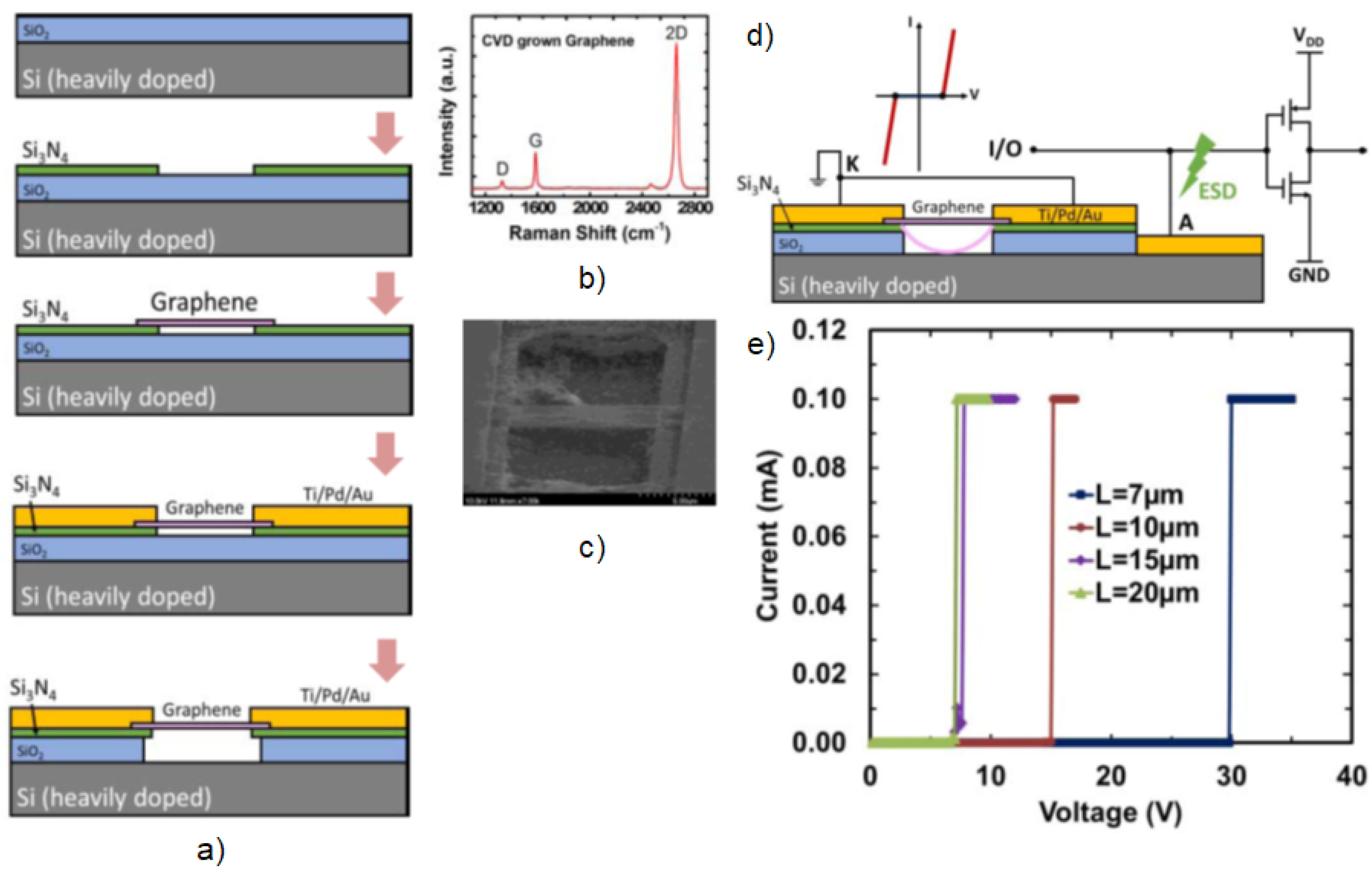
4.1. MEMS Switches
4.2. Mass Sensors
4.3. Pressure Sensors
4.4. Other Applications
5. Scaling Graphene Production
5.1. Manufacturing
5.2. Intrinsic Defects
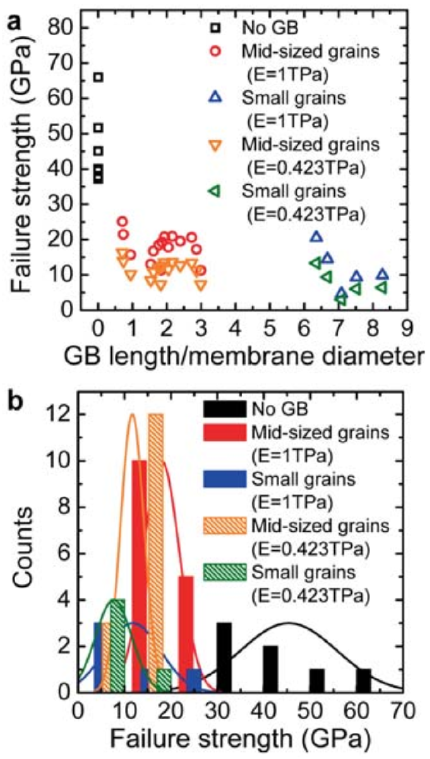
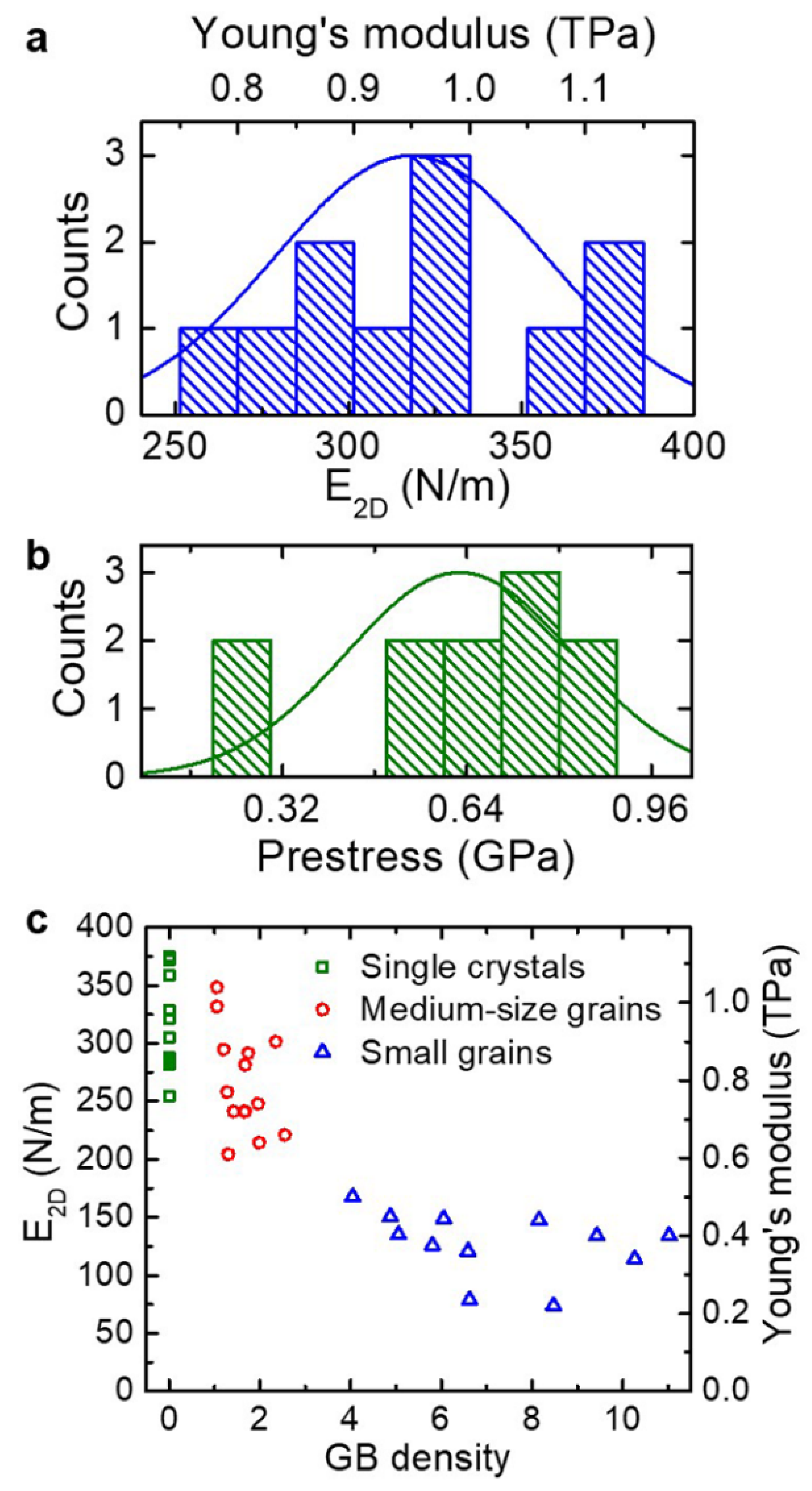
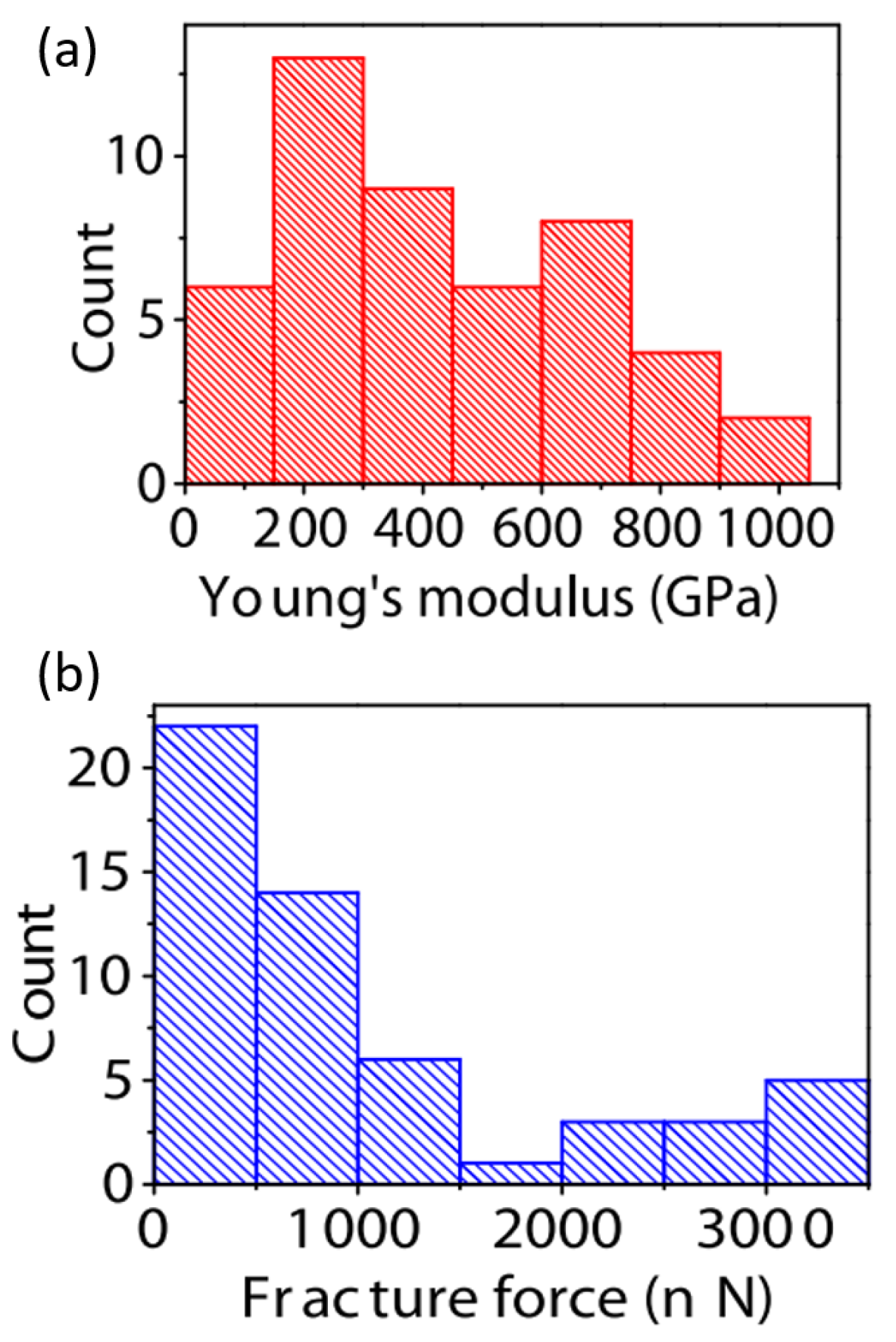
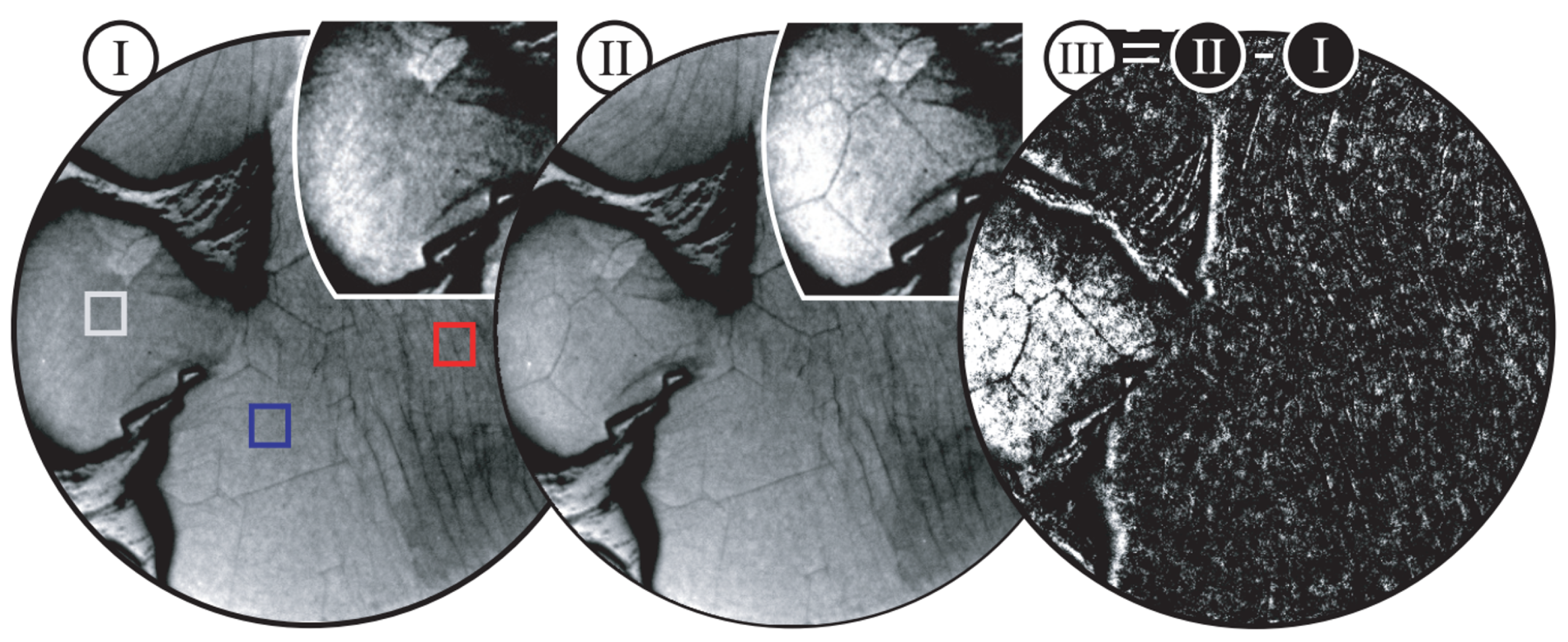
5.2.1. Graphene Grain Boundary Effects
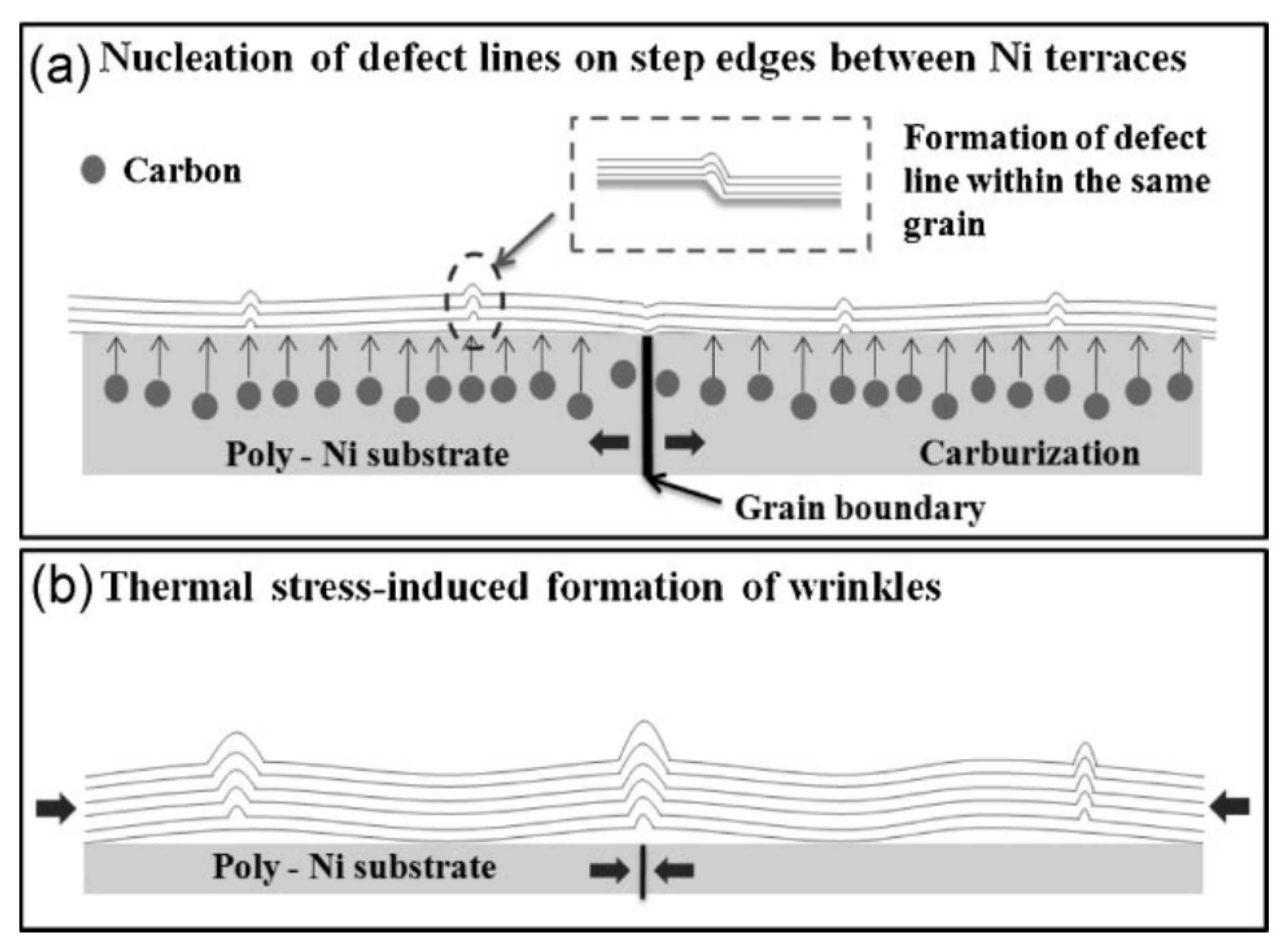
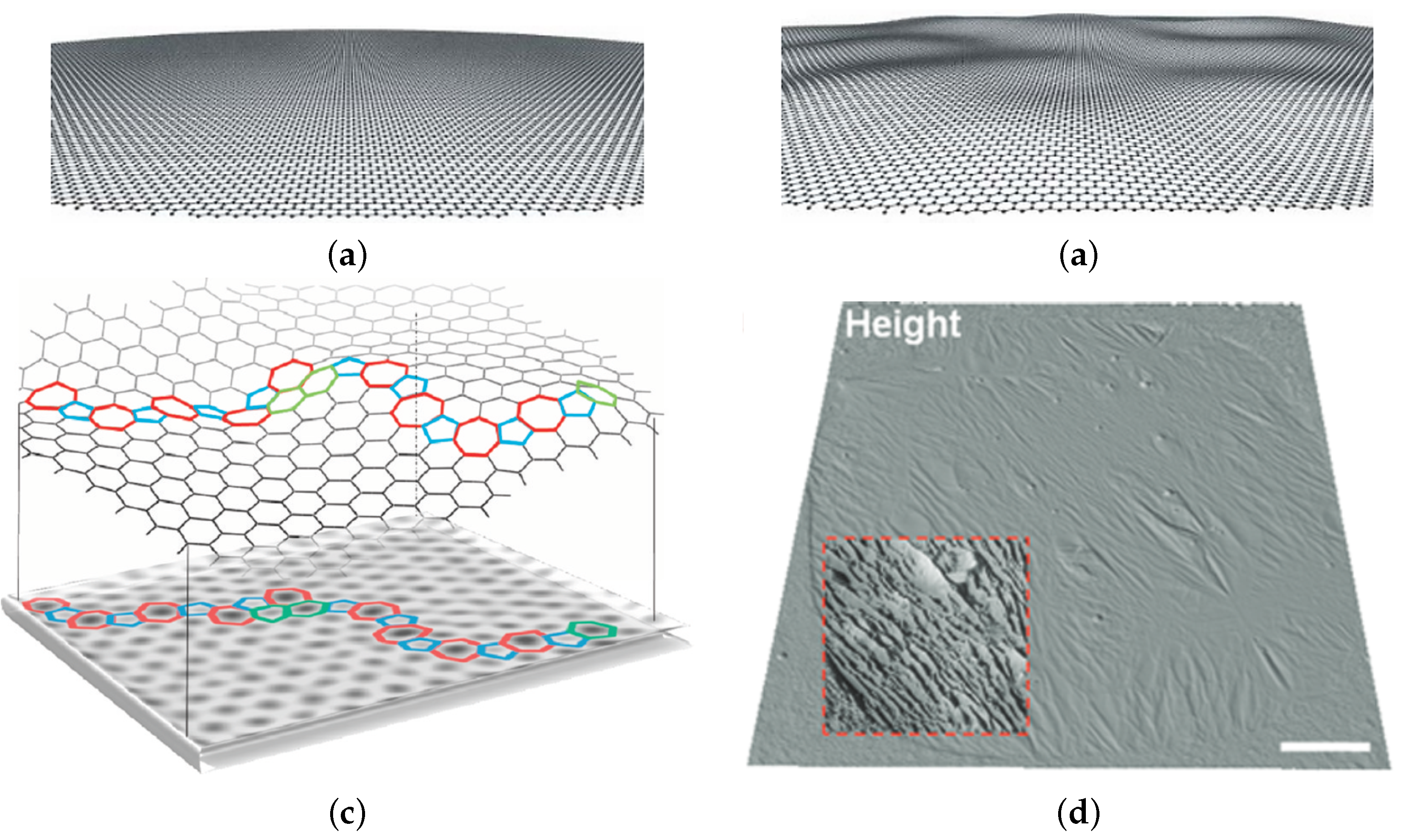
5.2.2. Wrinkles and Ripples
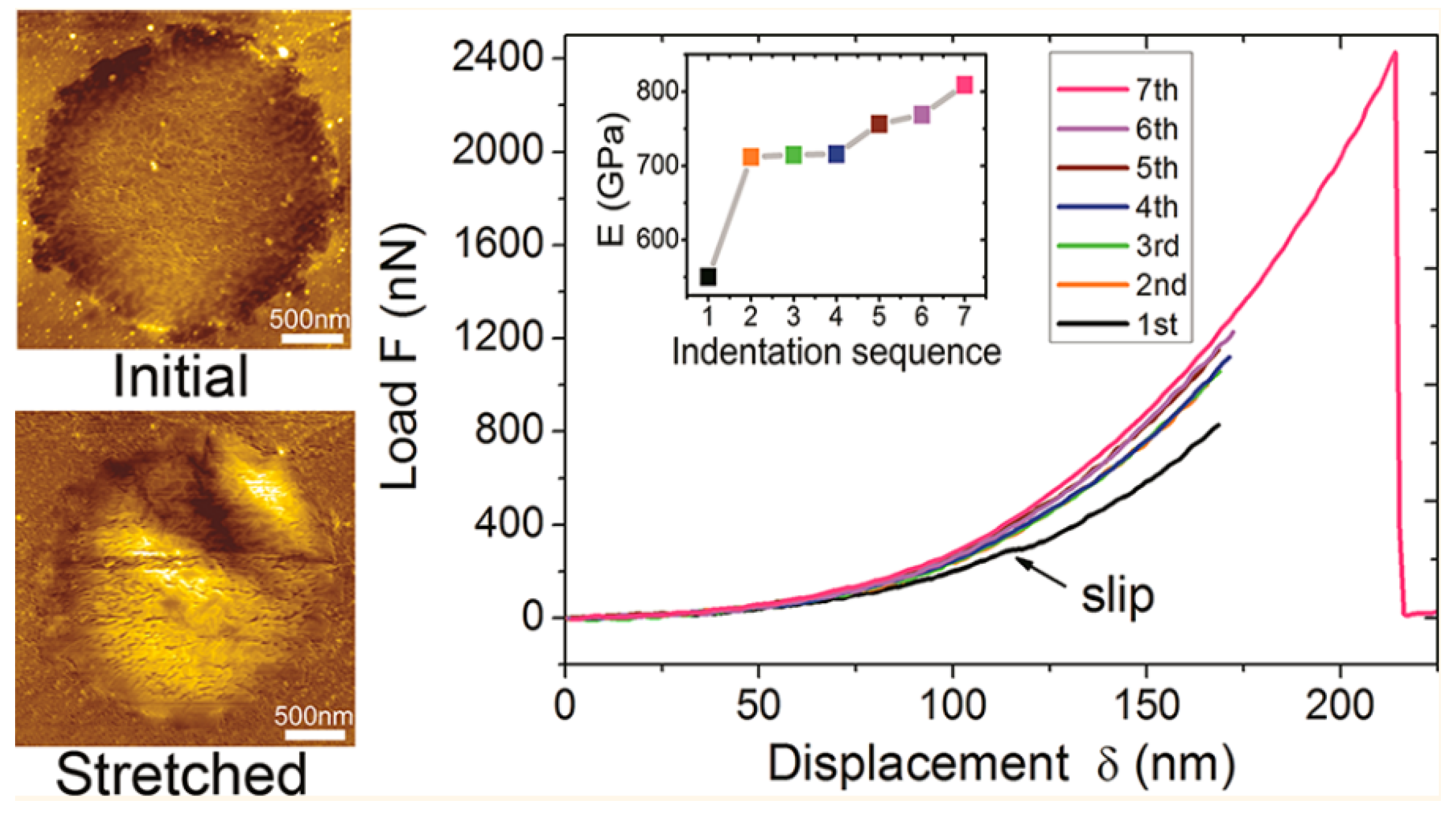
5.2.3. Voids and Other Defects
5.3. Importance of Repeatability
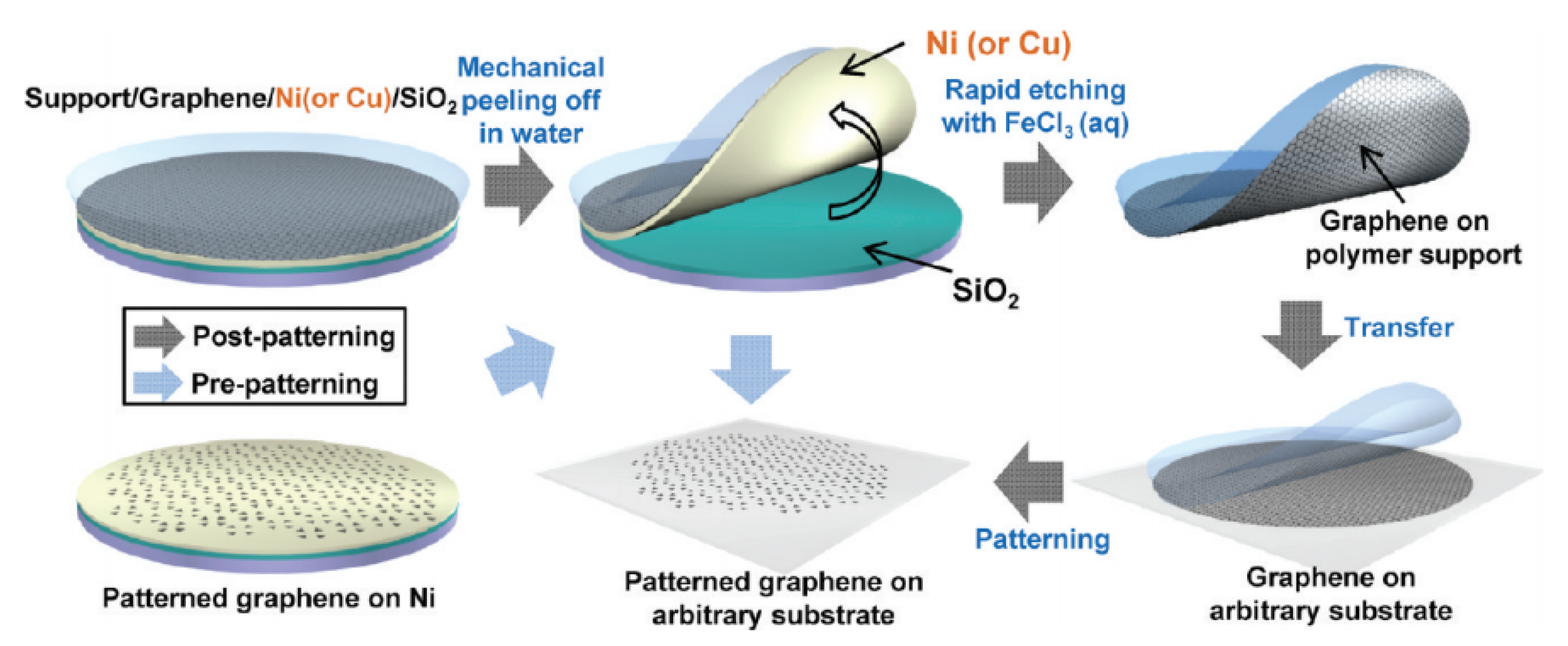
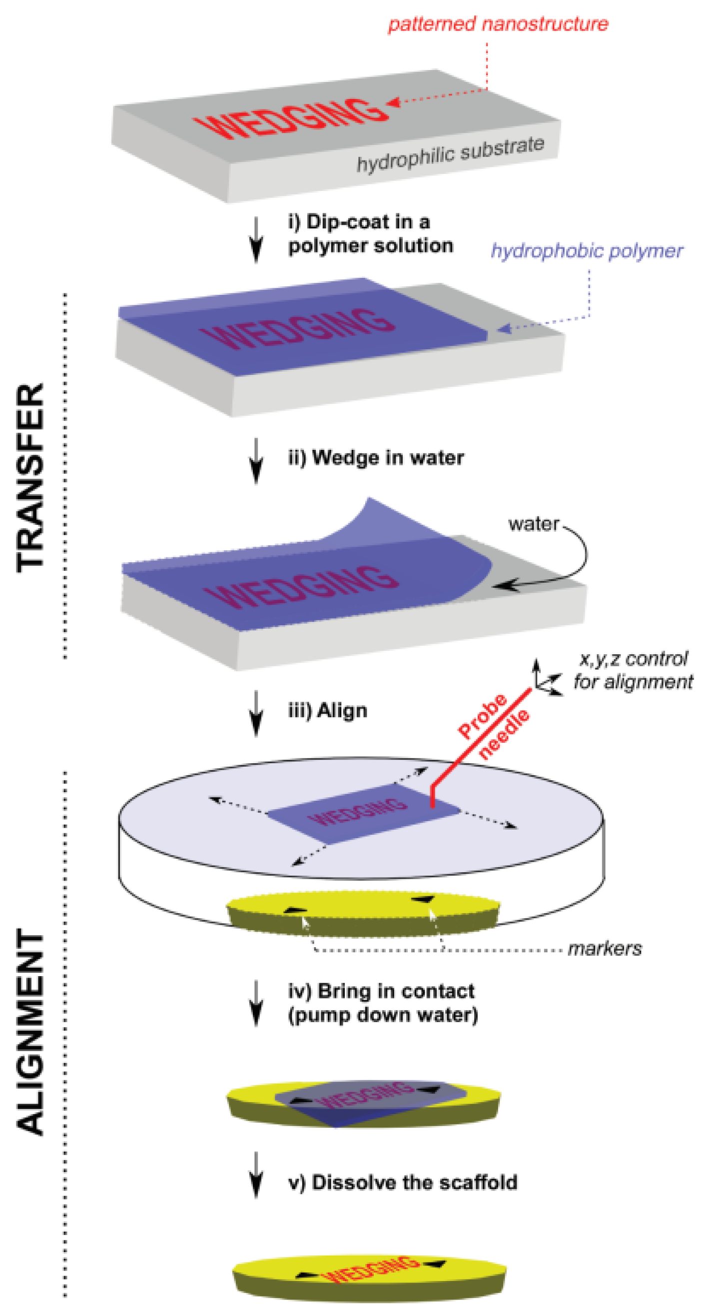
Methods of Graphene Transfer
6. Proposed Solutions
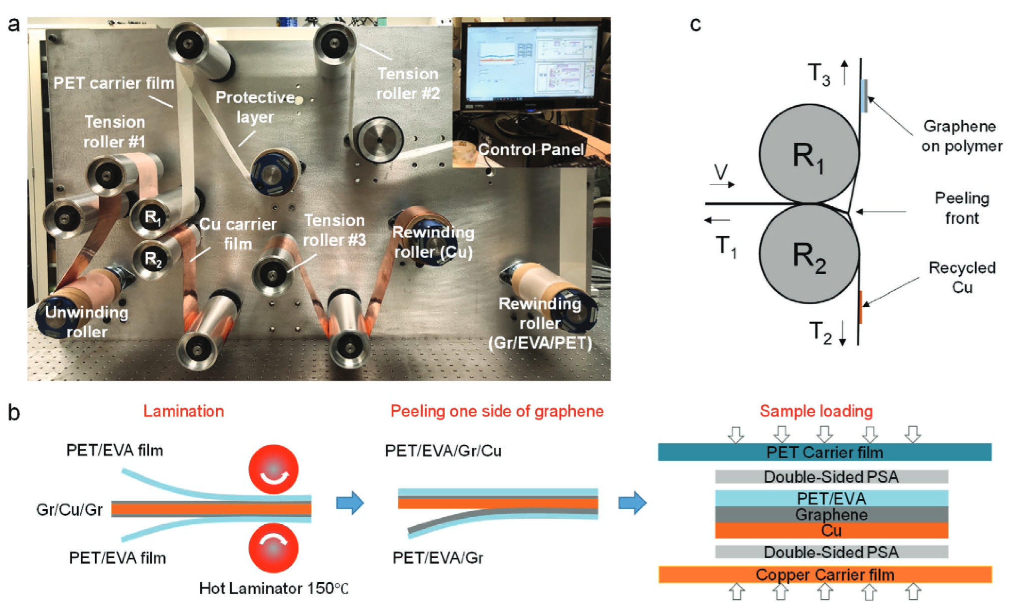
6.1. Roll-to-Roll (R2R) Processing
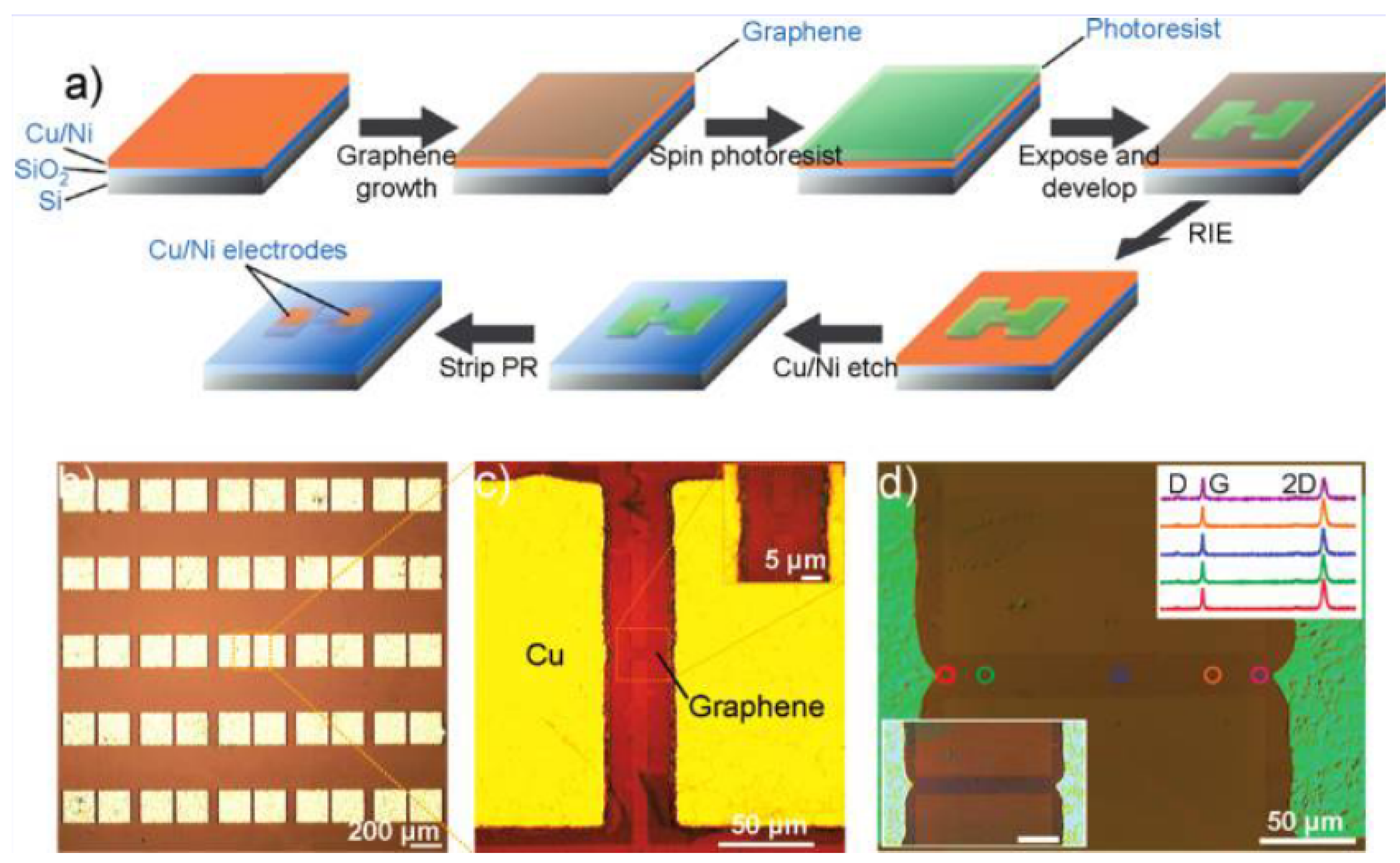
6.2. Transfer-Free, Graphene Growth on Thin-Films
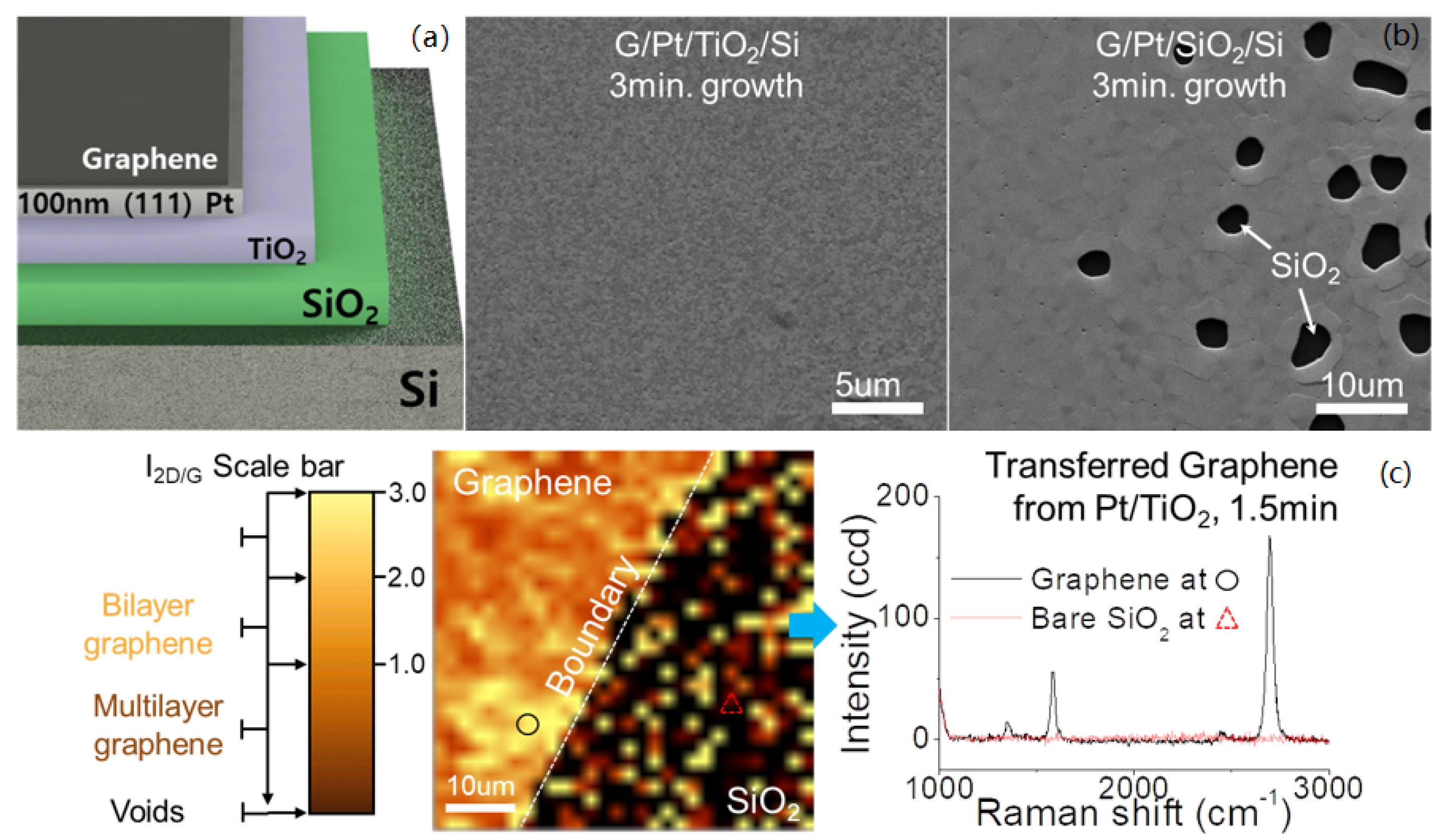
6.3. Low Temperature Growth of Graphene
6.4. Production of High Quality Single Crystalline Graphene in Large Scale
6.4.1. Substrate Engineering for Single-Seed Growth for Single Crystal Graphene (SCG)
6.4.2. Multi-Seed Growth for SCG
6.5. Other Approaches
7. Conclusions and Future Perspectives
Author Contributions
Funding
Conflicts of Interest
Abbreviations
| MEMS/NEMS | Microelectromechanical System/Nano-electromechanical System |
| CVD | Chemical Vapor Deposition |
| PMMA | Polymethyl methacrylate |
| PDMS | Polydimethylsiloxane |
| SCG | Single-Crystalline Graphene |
| PCG | Poly-Crystalline Graphene |
| GO | Graphene Oxide |
| rGO | Reduced Graphene Oxide |
References
- Lee, C.; Wei, X.; Kysar, J.W.; Hone, J. Measurement of the Elastic Properties and Intrinsic Strength of Monolayer Graphene. Science 2008, 321, 385–389. [Google Scholar] [CrossRef] [PubMed]
- Bolotin, K.I.; Sikes, K.J.; Hone, J.; Stormer, H.L.; Kim, P. Temperature-dependent transport in suspended graphene. Phys. Rev. Lett. 2008, 101, 1–4. [Google Scholar] [CrossRef] [PubMed] [Green Version]
- Geim, A.K. Graphene: Status and prospects. Science 2009, 324, 1530. [Google Scholar] [CrossRef] [PubMed] [Green Version]
- Xin, H.; Li, W. A review on high throughput roll-to-roll manufacturing of chemical vapor deposition graphene. Appl. Phys. Rev. 2018, 5, 031105. [Google Scholar] [CrossRef]
- Isacsson, A.; Cummings, A.W.; Colombo, L.; Colombo, L.; Kinaret, J.M.; Roche, S. Scaling properties of polycrystalline graphene: A review. 2D Materials 2017, 4, 012002. [Google Scholar] [CrossRef]
- Tan, H.; Wang, D.; Guo, Y. Thermal Growth of Graphene: A Review. Coatings 2018, 8, 40. [Google Scholar] [CrossRef] [Green Version]
- Levchenko, I.; Ostrikov, K.; Zheng, J.; Li, X.; Keidar, M.; Teo, K.B.K. Scalable graphene production: Perspectives and challenges of plasma applications w. Nanoscale 2016, 8, 10511–10527. [Google Scholar] [CrossRef]
- Cho, J.H.; Sun, G.; Cullinan, M. A method to manufacture repeatible graphene-based nems devices at the wafer-scale. In Proceedings of the ASME 2016 11th International Manufacturing Science and Engineering Conference (MSEC 2016), Blacksburg, VA, USA, 27 June 27–1 July 2016; Volume 1, pp. 1–6. [Google Scholar] [CrossRef]
- Wallace, P.R. The Band Theory of Graphite. Phys. Rev. 1947, 71, 452–457. [Google Scholar] [CrossRef]
- Novoselov, K.S.; Geim, A.K.; Morozov, S.V.; Jiang, D.; Zhang, Y.; Dubonos, S.V.; Grigorieva, I.V.; Firsov, A.A. Electric Field Effect in Atomically Thin Carbon Films. Phys. Rev. Lett. 2004, 306, 666–669. [Google Scholar] [CrossRef] [Green Version]
- Khan, Z.H.; Kermany, A.R.; Öchsner, A.; Iacopi, F. Mechanical and electromechanical properties of graphene and their potential application in MEMS. J. Phys. D Appl. Phys. 2017, 50, 053003. [Google Scholar] [CrossRef] [Green Version]
- Cao, Q.; Geng, X.; Wang, H.; Wang, P.; Liu, A.; Lan, Y.; Peng, Q. A review of current development of graphene mechanics. Crystals 2018, 8, 357. [Google Scholar] [CrossRef] [Green Version]
- Castro Neto, A.H.; Guinea, F.; Peres, N.M.R.; Novoselov, K.S.; Geim, A.K. The electronic properties of graphene. Rev. Mod. Phys. 2009, 81, 109–162. [Google Scholar] [CrossRef] [Green Version]
- Wong, H.S.P.; Akinwande, D. Carbon Nanotube and Graphene Device Physics; Cambridge University Press: Cambridge, UK, 2011. [Google Scholar]
- Kuo, W.S.; Tai, N.H.; Chang, T.W. Deformation and fracture in graphene nanosheets. Compos. Part A Appl. Sci. Manuf. 2013, 51, 56–61. [Google Scholar] [CrossRef]
- Jung, M.; Rickhaus, P.; Zihlmann, S.; Eichler, A.; Makk, P.; Schönenberger, C. GHz nanomechanical resonator in an ultraclean suspended graphene p–n junction. Nanoscale 2019, 11, 4355–4361. [Google Scholar] [CrossRef] [Green Version]
- Lemme, M.C.; Wagner, S.; Lee, K.; Fan, X.; Verbiest, G.J.; Wittmann, S.; Lukas, S.; Dolleman, R.J.; Niklaus, F.; van der Zant, H.S.J.; et al. Nanoelectromechanical Sensors Based on Suspended 2D Materials. Research 2020, 2020, 8748602. [Google Scholar] [CrossRef]
- Bolotin, K.I.; Sikes, K.; Jiang, Z.; Klima, M.; Fudenberg, G.; Hone, J.; Kim, P.; Stormer, H. Ultrahigh electron mobility in suspended graphene. Solid State Commun. 2008, 146, 351–355. [Google Scholar] [CrossRef] [Green Version]
- Lawal, A.T. Graphene-based nano composites and their applications. A review. Biosens. Bioelectron. 2019, 141, 111384. [Google Scholar] [CrossRef]
- Balandin, A.A.; Ghosh, S.; Bao, W.; Calizo, I.; Teweldebrhan, D.; Miao, F.; Lau, C.N. Superior thermal conductivity of single-layer graphene. Nano Lett. 2008, 8, 902–907. [Google Scholar] [CrossRef] [PubMed]
- Seol, J.H.; Jo, I.; Moore, A.L.; Lindsay, L.; Aitken, Z.H.; Pettes, M.T.; Li, X.; Yao, Z.; Huang, R.; Broido, D.; et al. Two-dimensional phonon transport in supported graphene. Science 2010, 328, 213–216. [Google Scholar] [CrossRef] [PubMed] [Green Version]
- Mounet, N.; Marzari, N. First-principles determination of the structural, vibrational and thermodynamic properties of diamond, graphite, and derivatives. Phys. Rev. B 2005, 71, 205214. [Google Scholar] [CrossRef] [Green Version]
- Bao, W.; Miao, F.; Chen, Z.; Zhang, H.; Jang, W.; Dames, C.; Lau, C.N. Controlled ripple texturing of suspended graphene and ultrathin graphite membranes. Nat. Nanotechnol. 2009, 4, 562–566. [Google Scholar] [CrossRef] [Green Version]
- Yoon, D.; Son, Y.W.; Cheong, H. Negative thermal expansion coefficient of graphene measured by Raman spectroscopy. Nano Lett. 2011, 11, 3227–3231. [Google Scholar] [CrossRef] [PubMed] [Green Version]
- Ong, M.T.; Reed, E.J. Engineered piezoelectricity in graphene. ACS Nano 2012, 6, 1387–1394. [Google Scholar] [CrossRef] [PubMed]
- Wang, X.; Tian, H.; Xie, W.; Shu, Y.; Mi, W.T.; Mohammad, M.A.; Xie, Q.Y.; Yang, Y.; Xu, J.B.; Ren, T.L. Observation of a giant two-dimensional band-piezoelectric effect on biaxial-strained graphene. NPG Asia Mater. 2015, 7, e154. [Google Scholar] [CrossRef] [Green Version]
- Da Cunha Rodrigues, G.; Zelenovskiy, P.; Romanyuk, K.; Luchkin, S.; Kopelevich, Y.; Kholkin, A. Strong piezoelectricity in single-layer graphene deposited on SiO2 grating substrates. Nat. Commun. 2015, 6, 7572. [Google Scholar] [CrossRef]
- Zhu, S.E.; Ghatkesar, M.K.; Zhang, C.; Janssen, G. Graphene based piezoresistive pressure sensor. Appl. Phys. Lett. 2013, 102. [Google Scholar] [CrossRef] [Green Version]
- Hosseinzadegan, H.; Todd, C.; Lal, A.; Pandey, M.; Levendorf, M.; Park, J. Graphene has ultra high piezoresistive gauge factor. In Proceedings of the IEEE 25th International Conference on Micro Electro Mechanical Systems (MEMS), Paris, France, 29 January–2 February 2012; pp. 611–614. [Google Scholar] [CrossRef]
- Judy, J.W. Microelectromechanical systems ({MEMS}): Fabrication, design and applications. Smart Mater. Struct. 2001, 10, 1115–1134. [Google Scholar] [CrossRef] [Green Version]
- Qu, H. CMOS MEMS Fabrication Technologies and Devices. Micromachines 2016, 7, 14. [Google Scholar] [CrossRef] [Green Version]
- Elders, J.; Spiering, V.; Walsh, S. Microsystems Technology (MST) and MEMS Applications: An Overview. MRS Bull. 2001, 26, 312–315. [Google Scholar] [CrossRef]
- Franke, A.E.; King, T.J.; Howe, R.T. Integrated MEMS Technologies. MRS Bull. 2001, 26, 291–295. [Google Scholar] [CrossRef]
- Arney, S. Designing for MEMS Reliability. MRS Bull. 2001, 26, 296–299. [Google Scholar] [CrossRef]
- Song, P.; Ma, Z.; Ma, J.; Yang, L.; Wei, J.; Zhao, Y.; Zhang, M.; Yang, F.; Wang, X. Recent Progress of Miniature MEMS Pressure Sensors. Micromachines 2020, 11, 56. [Google Scholar] [CrossRef] [Green Version]
- Fragiacomo, G.; Reck, K.; Lorenzen, L.; Thomsen, E.V. Novel Designs for Application Specific MEMS Pressure Sensors. Sensors 2010, 10, 9541–9563. [Google Scholar] [CrossRef] [PubMed] [Green Version]
- Dong, Y.; Zwahlen, P.; Nguyen, A.M.; Frosio, R.; Rudolf, F. Ultra-high precision MEMS accelerometer. In Proceedings of the 2011 16th International Solid-State Sensors, Actuators and Microsystems Conference, Beijing, China, 5–9 June 2011; pp. 695–698. [Google Scholar] [CrossRef]
- Zou, X.; Seshia, A.A. A high-resolution resonant MEMS accelerometer. In Proceedings of the 2015 Transducers—2015 18th International Conference on Solid-State Sensors, Actuators and Microsystems (TRANSDUCERS), Anchorage, AK, USA, 21–25 June 2015; pp. 1247–1250. [Google Scholar] [CrossRef]
- Tanaka, M. An industrial and applied review of new MEMS devices features. Microelectron. Eng. 2007, 84, 1341–1344. [Google Scholar] [CrossRef]
- Bogue, R. Recent developments in MEMS sensors: A review of applications, markets and technologies. Sens. Rev. 2013, 33, 300–304. [Google Scholar] [CrossRef]
- Song, Y.; Panas, R.M.; Hopkins, J.B. A review of micromirror arrays. Precis. Eng. 2018, 51, 729–761. [Google Scholar] [CrossRef]
- Singh, J.; Teo, J.H.S.; Xu, Y.; Premachandran, C.S.; Chen, N.; Kotlanka, R.; Olivo, M.; Sheppard, C.J.R. A two axes scanning {SOI} {MEMS} micromirror for endoscopic bioimaging. J. Micromechanics Microengineering 2007, 18, 25001. [Google Scholar] [CrossRef]
- Cheng, Y.C.; Dai, C.L.; Lee, C.Y.; Chen, P.H.; Chang, P.Z. A MEMS micromirror fabricated using CMOS post-process. Sensors Actuators A Phys. 2005, 120, 573–581. [Google Scholar] [CrossRef]
- Hu, F.; Yao, J.; Qiu, C.; Ren, H. A MEMS micromirror driven by electrostatic force. J. Electrost. 2010, 68, 237–242. [Google Scholar] [CrossRef]
- Ekinci, K.L.; Roukes, M.L. Nanoelectromechanical systems. Rev. Sci. Instrum. 2005, 76, 61101. [Google Scholar] [CrossRef] [Green Version]
- Craighead, H.G. Nanoelectromechanical Systems. Science 2000, 290, 1532–1535. [Google Scholar] [CrossRef] [Green Version]
- Cimalla, V.; Niebelschütz, F.; Tonisch, K.; Foerster, C.; Brueckner, K.; Cimalla, I.; Friedrich, T.; Pezoldt, J.; Stephan, R.; Hein, M.; et al. Nanoelectromechanical devices for sensing applications. Sens. Actuators B Chem. 2007, 126, 24–34. [Google Scholar] [CrossRef]
- Ekinci, K.L.; Yang, Y.T.; Roukes, M.L. Ultimate limits to inertial mass sensing based upon nanoelectromechanical systems. J. Appl. Phys. 2004, 95, 2682–2689. [Google Scholar] [CrossRef] [Green Version]
- Melzak, J.M. Silicon carbide for RF MEMS. In Proceedings of the IEEE MTT-S International Microwave Symposium Digest, Philadelphia, PA, USA, 8–13 June 2003; Volume 3, pp. 1629–1632. [Google Scholar] [CrossRef]
- Sharma, P.; Perruisseau-Carrier, J.; Moldovan, C.; Ionescu, A.M. Electromagnetic Performance of RF NEMS Graphene Capacitive Switches. IEEE Trans. Nanotechnol. 2014, 13, 70–79. [Google Scholar] [CrossRef]
- Basu, A.; Adams, G.G.; McGruer, N.E. A review of micro-contact physics, materials, and failure mechanisms in direct-contact {RF} {MEMS} switches. J. Micromechanics Microengineering 2016, 26, 104004. [Google Scholar] [CrossRef]
- Weinberg, M.; Candler, R.; Chandorkar, S.; Varsanik, J.; Kenny, T.; Duwel, A. Energy loss in MEMS resonators and the impact on inertial and RF devices. In Proceedings of the TRANSDUCERS 2009—2009 International Solid-State Sensors, Actuators and Microsystems Conference, Denver, CO, USA, 21–25 June 2009; pp. 688–695. [Google Scholar] [CrossRef]
- Vaddi, R.; Pott, V.; Chua, G.L.; Lin, J.T.M.; Kim, T.T. Design and Scalability of a Memory Array Utilizing Anchor-Free Nanoelectromechanical Nonvolatile Memory Device. IEEE Electron Device Lett. 2012, 33, 1315–1317. [Google Scholar] [CrossRef] [Green Version]
- Jang, W.W.; Yoon, J.B.; Kim, M.S.; Lee, J.M.; Kim, S.M.; Yoon, E.J.; Cho, K.H.; Lee, S.Y.; Choi, I.H.; Kim, D.W.; et al. NEMS switch with 30nm-thick beam and 20nm-thick air-gap for high density non-volatile memory applications. Solid-State Electron. 2008, 52, 1578–1583. [Google Scholar] [CrossRef]
- Ranganathan, V.; He, T.; Rajgopal, S.; Mehregany, M.; Feng, P.X.L.; Bhunia, S. Nanomechanical non-volatile memory for computing at extreme. In Proceedings of the 2013 IEEE/ACM International Symposium on Nanoscale Architectures (NANOARCH), Brooklyn, NY, USA, 15–17 July 2013; pp. 44–45. [Google Scholar] [CrossRef]
- Xu, D.; Wang, Y.; Xiong, B.; Li, T. MEMS-based thermoelectric infrared sensors: A review. Front. Mech. Eng. 2017, 12, 557–566. [Google Scholar] [CrossRef]
- Hui, Y.; Rinaldi, M. High performance NEMS resonant infrared detector based on an aluminum nitride nano-plate resonator. In Proceedings of the 2013 Transducers Eurosensors XXVII: The 17th International Conference on Solid-State Sensors, Actuators and Microsystems (TRANSDUCERS EUROSENSORS XXVII), Barcelona, Spain, 16–20 June 2013; pp. 968–971. [Google Scholar] [CrossRef]
- Qian, Z.; Hui, Y.; Liu, F.; Kang, S.; Kar, S.; Rinaldi, M. Graphene–aluminum nitride NEMS resonant infrared detector. Microsystems Nanoeng. 2016, 2, 16026. [Google Scholar] [CrossRef]
- Lai, J.J.; Liang, H.F.; Peng, Z.L.; Yi, X.; Zhai, X.F. {MEMS} integrated narrow band infrared emitter and detector for infrared gas sensor. J. Phys. Conf. Ser. 2011, 276, 12129. [Google Scholar] [CrossRef] [Green Version]
- Yoon, J.H.; Kim, J.S. Design and Fabrication of a MEMS-Based Gas Sensor. In Proceedings of the NEMS/MEMS Technology and Devices—ICMAT2009; Advanced Materials Research; Trans Tech Publications Ltd.: Stafa-Zurich, Switzerland, 2009; pp. 255–258. [Google Scholar] [CrossRef]
- Nagase, M.; Hibino, H.; Kageshima, H.; Yamaguchi, H. Graphene-Based Nano-Electro-Mechanical Switch with High On/Off Ratio. Appl. Phys. Express 2013, 6, 55101. [Google Scholar] [CrossRef]
- Ma, R.; Chen, Q.; Zhang, W.; Lu, F.; Wang, C.; Wang, A.; Xie, Y.; Tang, H. A Dual-Polarity Graphene NEMS Switch ESD Protection Structure. IEEE Electron Device Lett. 2016, 37, 674–676. [Google Scholar] [CrossRef]
- Jiang, S.; Shi, T.; Zhan, X.; Xi, S.; Long, H.; Gong, B.; Li, J.; Cheng, S.; Huang, Y.; Tang, Z. Scalable fabrication of carbon-based {MEMS}/{NEMS} and their applications: A review. J. Micromechanics Microengineering 2015, 25, 113001. [Google Scholar] [CrossRef]
- Cui, Z.; Gu, C. Nanofabrication Challenges for NEMS. In Proceedings of the 2006 1st IEEE International Conference on Nano/Micro Engineered and Molecular Systems, Zhuhai, China, 18–21 January 2006; pp. 607–610. [Google Scholar] [CrossRef]
- Feng, P.X.L. NEMS switches: Opportunities and challenges in emerging IC technologies. In Proceedings of the 2015 International Conference on IC Design Technology (ICICDT), Leuven, Belgium, 1–3 June 2015; pp. 1–6. [Google Scholar] [CrossRef]
- Villanueva, L.G.; Bausells, J.; Brugger, J. Grand Challenge in N/MEMS. Front. Mech. Eng. 2016, 1, 15. [Google Scholar] [CrossRef] [Green Version]
- Pinto, R.M.; Brito, P.; Chu, V.; Conde, J.P. Thin-film silicon MEMS for dynamic mass sensing in vacuum and air: Phase noise, allan deviation, mass sensitivity and limits of detection. J. Microelectromechanical Syst. 2019, 28, 390–400. [Google Scholar] [CrossRef]
- Bunch, J.S.; Zande, A.M.V.D.; Verbridge, S.S.; Frank, I.W.; Tanenbaum, D.M.; Parpia, J.M.; Craighead, H.G.; McEuen, P.L. Electromechanical resonators from graphene sheets. Science 2007, 315, 490–493. [Google Scholar] [CrossRef] [Green Version]
- Eichler, A.; Moser, J.; Chaste, J.; Zdrojek, M.; Bachtold, A.; Wilson-Rae, I.; Bachtold, A. Nonlinear damping in mechanical resonators made from carbon nanotubes and graphene. Nat. Nanotechnol. 2011, 6, 339–342. [Google Scholar] [CrossRef]
- Duan, K.; Li, L.; Hu, Y.; Wang, X. Pillared graphene as an ultra-high sensitivity mass sensor. Sci. Rep. 2017, 7, 14012. [Google Scholar] [CrossRef] [Green Version]
- Lee, H.L.; Yang, Y.C.; Chang, W.J. Mass detection using a graphene-based nanomechanical resonator. Jpn. J. Appl. Phys. 2013, 52, 025101. [Google Scholar] [CrossRef]
- Xiao, X.; Fan, S.C.; Li, C.; Xing, W.W. Stress-Insensitive Resonant Graphene Mass Sensing via Frequency Ratio. Sensors 2019, 19, 3027. [Google Scholar] [CrossRef] [Green Version]
- Or, P.; Dribin, D.; Devidas, T.R.; Zalic, A.; Watanabe, K.; Taniguchi, T.; May-Tal Beck, S.; Ron, G.; Steinberg, H. Graphene-based positron charge sensor. Appl. Phys. Lett. 2018, 113, 154101. [Google Scholar] [CrossRef]
- Neumann, C.; Volk, C.; Engels, S.; Stampfer, C. Graphene-based charge sensors. Nanotechnology 2013, 24, 444001. [Google Scholar] [CrossRef] [PubMed]
- Chen, C.; Deshpande, V.V.; Koshino, M.; Lee, S.; Gondarenko, A.; MacDonald, A.H.; Kim, P.; Hone, J. Modulation of mechanical resonance by chemical potential oscillation in graphene. Nat. Phys. 2016, 12, 240–244. [Google Scholar] [CrossRef] [Green Version]
- Weber, P.; Güttinger, J.; Noury, A.; Vergara-Cruz, J.; Bachtold, A. Force sensitivity of multilayer graphene optomechanical devices. Nat. Commun. 2016, 7, 12496. [Google Scholar] [CrossRef] [PubMed]
- Gooding, J.J. The Exciting World of Single Molecule Sensors. ACS Sensors 2016, 1, 1163–1164. [Google Scholar] [CrossRef] [Green Version]
- Kwon, O.K.; Kim, K.S.; Park, J.; Kang, J.W. Molecular dynamics modeling and simulations of graphene-nanoribbon-resonator-based nanobalance as yoctogram resolution detector. Comput. Mater. Sci. 2013, 67, 329–333. [Google Scholar] [CrossRef]
- Sazonova, V.; Yaish, Y.; Üstünel, H.; Roundy, D.; Arias, T.A.; McEuen, P.L. A tunable carbon nanotube electromechanical oscillator. Nature 2004, 431, 284–287. [Google Scholar] [CrossRef] [Green Version]
- Sone, H.; Fujinuma, Y.; Hosaka, S. Picogram mass sensor using resonance frequency shift of cantilever. Jpn. J. Appl. Phys. 2004, 43, 3648. [Google Scholar] [CrossRef]
- Ekinci, K.; Huang, X.; Roukes, M. Ultrasensitive nanoelectromechanical mass detection. Appl. Phys. Lett. 2004, 84, 4469–4471. [Google Scholar] [CrossRef] [Green Version]
- Chaste, J.; Eichler, A.; Moser, J.; Ceballos, G.; Rurali, R.; Bachtold, A. A nanomechanical mass sensor with yoctogram resolution. Nat. Nanotechnol. 2012, 7, 301–304. [Google Scholar] [CrossRef]
- Chen, C.; Rosenblatt, S.; Bolotin, K.I.; Kalb, W.; Kim, P.; Kymissis, I.; Stormer, H.L.; Heinz, T.F.; Hone, J.; Horst, L.; et al. Performance of monolayer graphene nanomechanical resonators with electrical readout. Nat. Nanotechnol. 2009, 4, 861–867. [Google Scholar] [CrossRef] [PubMed] [Green Version]
- Wong, C.L.; Annamalai, M.; Wang, Z.Q.; Palaniapan, M. Characterization of nanomechanical graphene drum structures. J. Micromechanics Microengineering 2010, 20, 115029. [Google Scholar] [CrossRef]
- Abadal, G.; Davis, Z.J.; Helbo, B.; Borrise, X.; Ruiz, R.; Boisen, A.; Campabadal, F.; Esteve, J.; Figueras, E.; Perez-Murano, F. Electromechanical model of a resonating nano-cantilever-based sensor for high-resolution and high-sensitivity mass detection. Nanotechnology 2001, 12, 100. [Google Scholar] [CrossRef]
- Singh, V.; Sengupta, S.; Solanki, H.S.; Dhall, R.; Allain, A.; Dhara, S.; Pant, P.; Deshmukh, M.M. Probing thermal expansion of graphene and modal dispersion at low-temperature using graphene nanoelectromechanical systems resonators. Nanotechnology 2010, 21, 165204. [Google Scholar] [CrossRef] [PubMed] [Green Version]
- Lou, Z.; Chen, S.; Wang, L.; Jiang, K.; Shen, G. An ultra-sensitive and rapid response speed graphene pressure sensors for electronic skin and health monitoring. Nano Energy 2016, 23, 7–14. [Google Scholar] [CrossRef]
- Tian, H.; Shu, Y.; Wang, X.F.; Mohammad, M.A.; Bie, Z.; Xie, Q.Y.; Li, C.; Mi, W.T.; Yang, Y.; Ren, T.L. A Graphene-Based Resistive Pressure Sensor with Record-High Sensitivity in a Wide Pressure Range. Sci. Rep. 2015, 5, 8603. [Google Scholar] [CrossRef]
- Vollebregt, S.; Dolleman, R.J.; Zant, H.S.J.v.d.; Steeneken, P.G.; Sarro, P.M. Suspended graphene beams with tunable gap for squeeze-film pressure sensing. In Proceedings of the 2017 19th International Conference on Solid-State Sensors, Actuators and Microsystems (TRANSDUCERS), Kaohsiung, Taiwan, 18–22 June 2017; pp. 770–773. [Google Scholar] [CrossRef]
- Romijn, J.; Dolleman, R.J.; Singh, M.; van der Zant, H.S.J.; Steeneken, P.G.; Sarro, P.M.; Vollebregt, S. Multi-layer graphene pirani pressure sensors. Nanotechnology 2021, 32, 335501. [Google Scholar] [CrossRef]
- Bae, S.H.; Lee, Y.; Sharma, B.K.; Lee, H.J.; Kim, J.H.; Ahn, J.H. Graphene-based transparent strain sensor. Carbon 2013, 51, 236–242. [Google Scholar] [CrossRef]
- Wang, Y.; Wang, L.; Yang, T.; Li, X.; Zang, X.; Zhu, M.; Wang, K.; Wu, D.; Zhu, H. Wearable and Highly Sensitive Graphene Strain Sensors for Human Motion Monitoring. Adv. Funct. Mater. 2014, 24, 4666–4670. [Google Scholar] [CrossRef]
- Chun, S.; Choi, Y.; Park, W. All-graphene strain sensor on soft substrate. Carbon 2017, 116, 753–759. [Google Scholar] [CrossRef]
- Tian, H.; Shu, Y.; Cui, Y.L.; Mi, W.T.; Yang, Y.; Xie, D.; Ren, T.L. Scalable fabrication of high-performance and flexible graphene strain sensors. Nanoscale 2014, 6, 699–705. [Google Scholar] [CrossRef]
- Hurst, A.M.; Lee, S.; Cha, W.; Hone, J. A graphene accelerometer. In Proceedings of the 2015 28th IEEE International Conference on Micro Electro Mechanical Systems (MEMS), Estoril, Portugal, 18–22 January 2015; pp. 865–868. [Google Scholar] [CrossRef]
- Ahmadian, M.; Jafari, K.; Sharifi, M.J. Novel graphene-based optical MEMS accelerometer dependent on intensity modulation. ETRI J. 2018, 40, 794–801. [Google Scholar] [CrossRef]
- Ahmadian, M.; Jafari, K. A Graphene-Based Wide-Band MEMS Accelerometer Sensor Dependent on Wavelength Modulation. IEEE Sens. J. 2019, 19, 6226–6232. [Google Scholar] [CrossRef]
- Fan, X.; Forsberg, F.; Smith, A.D.; Schröder, S.; Wagner, S.; Östling, M.; Lemme, M.C.; Niklaus, F. Suspended Graphene Membranes with Attached Silicon Proof Masses as Piezoresistive Nanoelectromechanical Systems Accelerometers. Nano Lett. 2019, 19, 6788–6799. [Google Scholar] [CrossRef] [PubMed] [Green Version]
- Smith, A.; Niklaus, F.; Paussa, A.; Vaziri, S.; Fischer, A.C.; Sterner, M.; Forsberg, F.; Delin, A.; Esseni, D.; Palestri, P.; et al. Electromechanical piezoresistive sensing in suspended graphene membranes. Nano Lett. 2013, 13, 3237–3242. [Google Scholar] [CrossRef]
- Meena, K.V.; Sankar, A.R. Biomedical Catheters With Integrated Miniature Piezoresistive Pressure Sensors: A Review. IEEE Sens. J. 2021, 21, 10241–10290. [Google Scholar] [CrossRef]
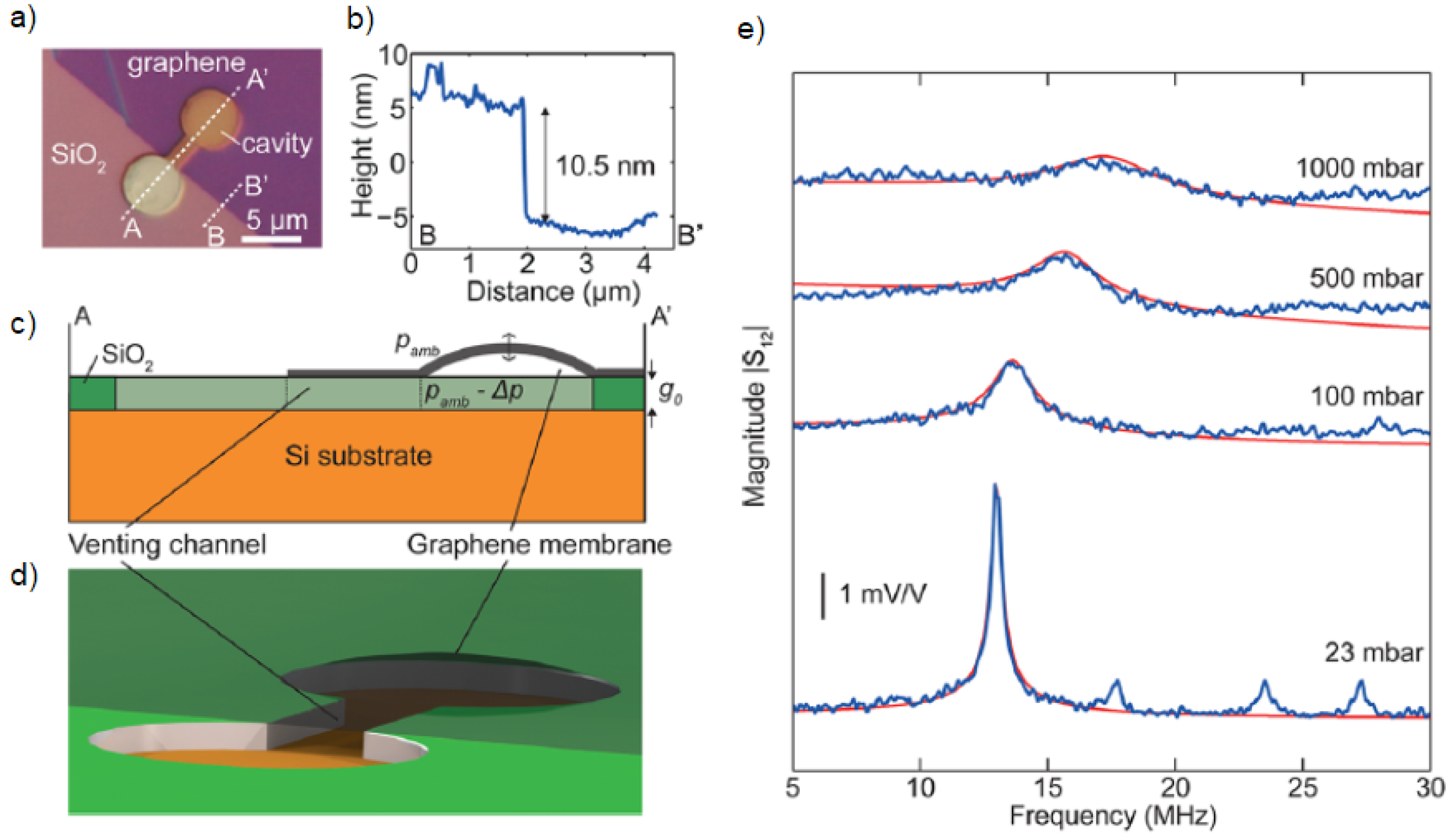
- Dolleman, R.J.; Davidovikj, D.; Cartamil-Bueno, S.J.; van der Zant, H.S.J.; Steeneken, P.G. Graphene Squeeze-Film Pressure Sensors. Nano Lett. 2016, 16, 568–571. [Google Scholar] [CrossRef] [Green Version]
- Rahman, S.H.A.; Soin, N.; Ibrahim, F. Design of graphene-based MEMS intracranial pressure sensor. In Proceedings of the 2016 IEEE International Symposium on Medical Measurements and Applications (MeMeA); 2016; pp. 1–5. [Google Scholar] [CrossRef]
- Tamersit, K.; Kotti, M.; Fakhfakh, M. A new pressure microsensor based on dual-gate graphene field-effect transistor with a vertically movable top-gate: Proposal, analysis, and optimization. AEU-Int. J. Electron. Commun. 2020, 124, 153346. [Google Scholar] [CrossRef]
- Zhao, J.; He, C.; Yang, R.; Shi, Z.; Cheng, M.; Yang, W.; Xie, G.; Wang, D.; Shi, D.; Zhang, G. Ultra-sensitive strain sensors based on piezoresistive nanographene films. Appl. Phys. Lett. 2012, 101, 063112. [Google Scholar] [CrossRef]
- Kim, Y.J.; Cha, J.Y.; Ham, H.; Huh, H.; So, D.S.; Kang, I. Preparation of piezoresistive nano smart hybrid material based on graphene. Curr. Appl. Phys. 2011, 11, S350–S352. [Google Scholar] [CrossRef]
- Davidovikj, D.; Scheepers, P.H.; van der Zant, H.S.J.; Steeneken, P.G. Static Capacitive Pressure Sensing Using a Single Graphene Drum. ACS Appl. Mater. Interfaces 2017, 9, 43205–43210. [Google Scholar] [CrossRef] [Green Version]
- Tian, H.; Ma, S.; Zhao, H.M.; Wu, C.; Ge, J.; Xie, D.; Yang, Y.; Ren, T.L. Flexible electrostatic nanogenerator using graphene oxide film. Nanoscale 2013, 5, 8951–8957. [Google Scholar] [CrossRef] [PubMed]
- Tarelho, J.P.G.; Soares dos Santos, M.P.; Ferreira, J.A.F.; Ramos, A.; Kopyl, S.; Kim, S.O.; Hong, S.; Kholkin, A. Graphene-based materials and structures for energy harvesting with fluids—A review. Mater. Today 2018, 21, 1019–1041. [Google Scholar] [CrossRef]
- Cohen-Tanugi, D.; Grossman, J.C. Nanoporous graphene as a reverse osmosis membrane: Recent insights from theory and simulation. Desalination 2015, 366, 59–70. [Google Scholar] [CrossRef] [Green Version]
- Jiang, D.E.; Cooper, V.R.; Dai, S. Porous graphene as the ultimate membrane for gas separation. Nano Lett. 2009, 9, 4019–4024. [Google Scholar] [CrossRef] [PubMed]
- Hauser, A.W.; Schwerdtfeger, P. Nanoporous graphene membranes for efficient 3He/4He separation. J. Phys. Chem. Lett. 2012, 3, 209–213. [Google Scholar] [CrossRef]
- O’Hern, S.C.; Boutilier, M.S.; Idrobo, J.C.; Song, Y.; Kong, J.; Laoui, T.; Atieh, M.; Karnik, R. Selective ionic transport through tunable subnanometer pores in single-layer graphene membranes. Nano Lett. 2014, 14, 1234–1241. [Google Scholar] [CrossRef] [Green Version]
- Fischbein, M.D.; Drndić, M. Electron beam nanosculpting of suspended graphene sheets. Appl. Phys. Lett. 2008, 93, 113107. [Google Scholar] [CrossRef] [Green Version]
- Bell, D.C.; Lemme, M.C.; Stern, L.A.; Williams, J.R.; Marcus, C.M. Precision cutting and patterning of graphene with helium ions. Nanotechnology 2009, 20, 455301. [Google Scholar] [CrossRef]
- Xu, P.; Yang, J.; Wang, K.; Zhou, Z.; Shen, P. Porous graphene: Properties, preparation, and potential applications. Chin. Sci. Bull. 2012, 57, 2948–2955. [Google Scholar] [CrossRef] [Green Version]
- Merchant, C.A.; Healy, K.; Wanunu, M.; Ray, V.; Peterman, N.; Bartel, J.; Fischbein, M.D.; Venta, K.; Luo, Z.; Johnson, A.C. DNA translocation through graphene nanopores. Nano Lett. 2010, 10, 2915–2921. [Google Scholar] [CrossRef]
- Garaj, S.; Hubbard, W.; Reina, A.; Kong, J.; Branton, D.; Golovchenko, J.A. Graphene as a subnanometre trans-electrode membrane. Nature 2010, 467, 190–193. [Google Scholar] [CrossRef] [PubMed]
- Novoselov, K.S.; Jiang, D.; Schedin, F.; Booth, T.J.; Khotkevich, V.V.; Morozov, S.V.; Geim, A.K. Two-dimensional atomic crystals. Proc. Natl. Acad. Sci. USA 2005, 102, 10451–10453. [Google Scholar] [CrossRef] [PubMed] [Green Version]
- Li, X.; Cai, W.; An, J.; Kim, S.; Nah, J.; Yang, D.; Piner, R.; Velamakanni, A.; Jung, I.; Tutuc, E.; et al. Large-Area Synthesis of High-Quality and Uniform Graphene Films on Copper Foils. Science 2009, 324, 1312–1314. [Google Scholar] [CrossRef] [PubMed] [Green Version]
- Kang, B.J.; Mun, J.H.; Hwang, C.Y.; Cho, B.J. Monolayer graphene growth on sputtered thin film platinum. J. Appl. Phys. 2009, 106, 104309. [Google Scholar] [CrossRef] [Green Version]
- Obraztsov, A.N.; Obraztsova, E.A.; Tyurnina, A.V.; Zolotukhin, A.A. Chemical vapor deposition of thin graphite films of nanometer thickness. Carbon 2007, 45, 2017–2021. [Google Scholar] [CrossRef]
- Lahiri, J.; Miller, T.S.; Ross, A.J.; Adamska, L.; Oleynik, I.I.; Batzill, M. Graphene growth and stability at nickel surfaces. New J. Phys. 2011, 13. [Google Scholar] [CrossRef]
- Mishra, N.; Forti, S.; Fabbri, F.; Martini, L.; McAleese, C.; Conran, B.; Whelan, P.R.; Shivayogimath, A.; Buß, L.; Falta, J.; et al. Going beyond copper: Wafer-scale synthesis of graphene on sapphire. Small 2019, 56127. [Google Scholar] [CrossRef] [Green Version]
- Li, X.; Cai, W.; Colombo, L.; Ruoff, R. Evolution of graphene growth on Ni and Cu by carbon isotope labeling. Nano Lett. 2009, 12, 1–15. [Google Scholar] [CrossRef] [Green Version]
- Ma, T.; Liu, Z.; Wen, J.; Gao, Y.; Ren, X.; Chen, H.; Jin, C.; Ma, X.L.; Xu, N.; Cheng, H.M.; et al. Tailoring the thermal and electrical transport properties of graphene films by grain size engineering. Nat. Commun. 2017, 8, 14486. [Google Scholar] [CrossRef]
- Tsen, A.W.; Brown, L.; Levendorf, M.P.; Ghahari, F.; Huang, P.Y.; Havener, R.W.; Ruiz-Vargas, C.S.; Muller, D.A.; Kim, P.; Park, J. Tailoring electrical transport across grain boundaries in polycrystalline graphene. Science 2012, 336, 1143–1146. [Google Scholar] [CrossRef] [Green Version]
- Lee, G.h.; Cooper, R.C.; An, S.J.; Lee, S.; Zande, A.M.V.D.; Petrone, N.; Hammerberg, A.G.; Lee, C.; Crawford, B.; Oliver, W.; et al. High-Strength Chemical-Vapor-Deposited Graphene and Grain Boundaries. Science 2013, 340, 1073–1076. [Google Scholar] [CrossRef] [PubMed]
- Suk, J.W.; Mancevski, V.; Hao, Y.; Liechti, K.M.; Ruoff, R.S. Fracture of polycrystalline graphene membranes by in situ nanoindentation in a scanning electron microscope. Phys. Status Solidi-Rapid Res. Lett. 2015, 9, 564–569. [Google Scholar] [CrossRef]
- Falin, A.; Cai, Q.; Santos, E.J.; Scullion, D.; Qian, D.; Zhang, R.; Yang, Z.; Huang, S.; Watanabe, K.; Taniguchi, T.; et al. Mechanical properties of atomically thin boron nitride and the role of interlayer interactions. Nat. Commun. 2017, 8, 15815. [Google Scholar] [CrossRef] [PubMed] [Green Version]
- Ruiz-Vargas, C.S.; Zhuang, H.L.; Huang, P.Y.; Van Der Zande, A.M.; Garg, S.; McEuen, P.L.; Muller, D.A.; Hennig, R.G.; Park, J. Softened elastic response and unzipping in chemical vapor deposition graphene membranes. Nano Lett. 2011, 11, 2259–2263. [Google Scholar] [CrossRef]
- Rasool, H.I.; Ophus, C.; Klug, W.S.; Zettl, A.; Gimzewski, J.K. Measurement of the intrinsic strength of crystalline and polycrystalline graphene. Nat. Commun. 2013, 4, 2811. [Google Scholar] [CrossRef]
- Suk, J.W.; Hao, Y.; Liechti, K.M.; Ruoff, R.S. Impact of Grain Boundaries on the Elastic Behavior of Transferred Polycrystalline Graphene. Chem. Mater. 2020, 32, 6078–6084. [Google Scholar] [CrossRef]
- Lin, Q.Y.; Zeng, Y.H.; Liu, D.; Jing, G.Y.; Liao, Z.M.; Yu, D. Step-by-step fracture of two-layer stacked graphene membranes. ACS Nano 2014, 8, 10246–10251. [Google Scholar] [CrossRef]
- Morozov, S.V.; Novoselov, K.S.; Katsnelson, M.I.; Schedin, F.; Elias, D.C.; Jaszczak, J.A.; Geim, A.K. Giant intrinsic carrier mobilities in graphene and its bilayer. Phys. Rev. Lett. 2008, 100, 11–14. [Google Scholar] [CrossRef] [Green Version]
- Zhang, Y.; Tang, T.T.; Girit, C.; Hao, Z.; Martin, M.C.; Zettl, A.; Crommie, M.F.; Shen, Y.R.; Wang, F. Direct observation of a widely tunable bandgap in bilayer graphene. Nature 2009, 459, 820–823. [Google Scholar] [CrossRef]
- Zhou, Q.; Zettl, A. Electrostatic graphene loudspeaker. Appl. Phys. Lett. 2013, 102, 966–985. [Google Scholar] [CrossRef] [Green Version]
- Cho, J.H.; Na, S.R.; Park, S.; Akinwande, D.; Liechti, K.M.; Cullinan, M.A. Controlling the number of layers in graphene using the growth pressure. Nanotechnology 2019, 30. [Google Scholar] [CrossRef] [PubMed] [Green Version]
- Huang, C.M.; Sarathivasan, A.S.; Huang, Y.; Doraiswami, R.; Osterman, M.; Pecht, M. MEMS reliability. Mems Packag. 2018, 12, 279–343. [Google Scholar] [CrossRef]
- Zhang, T.; Li, X.; Gao, H. Fracture of graphene: A review. Int. J. Fract. 2015, 196, 1–31. [Google Scholar] [CrossRef]
- Zhang, P.; Ma, L.; Fan, F.; Zeng, Z.; Peng, C.; Loya, P.E.; Liu, Z.; Gong, Y.; Zhang, J.; Zhang, X.; et al. Fracture toughness of graphene. Nat. Commun. 2014, 5, 3782. [Google Scholar] [CrossRef] [Green Version]
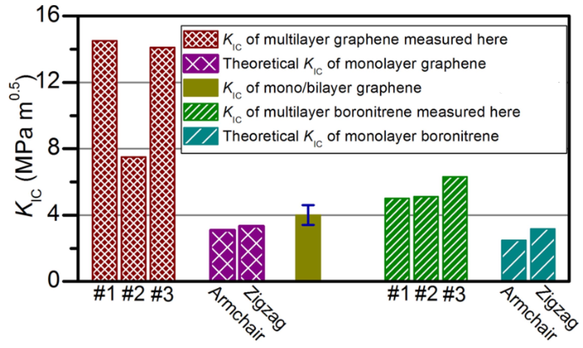
- Wei, X.; Xiao, S.; Li, F.; Tang, D.M.; Chen, Q.; Bando, Y.; Golberg, D. Comparative fracture toughness of multilayer graphenes and boronitrenes. Nano Lett. 2015, 15, 689–694. [Google Scholar] [CrossRef]
- Yakobson, B.I.; Ding, F. Observational geology of graphene, at the nanoscale. ACS Nano 2011, 5, 1569–1574. [Google Scholar] [CrossRef]
- Wei, Y.; Wu, J.; Yin, H.; Shi, X.; Yang, R.; Dresselhaus, M. The nature of strength enhancement and weakening by pentagong-heptagon defects in graphene. Nat. Mater. 2012, 11, 759–763. [Google Scholar] [CrossRef]
- Wu, J.; Cao, P.; Zhang, Z.; Ning, F.; Zheng, S.S.; He, J.; Zhang, Z. Grain-Size-Controlled Mechanical Properties of Polycrystalline Monolayer MoS2. Nano Lett. 2018, 18, 1543–1552. [Google Scholar] [CrossRef]
- Rao, R.; Pierce, N.; Xu, Q.; Harutyunyan, A.R. Probing inhomogeneous doping in overlapped graphene grain boundaries by Raman spectroscopy. Carbon 2014, 80, 513–522. [Google Scholar] [CrossRef]
- Min, S.Y.; Cho, C.; Shim, G.W.; Park, I.J.; Jung, D.Y.; Woo, Y.; Lee, J.Y.; Choi, S.Y. Two-dimensional sheet resistance model for polycrystalline graphene with overlapped grain boundaries. FlatChem 2018, 7, 19–25. [Google Scholar] [CrossRef]
- Mun, S.C.; Park, J.J.; Park, Y.T.; Kim, D.Y.; Lee, S.W.; Cobos, M.; Ye, S.J.; Macosko, C.W.; Park, O.O. High electrical conductivity and oxygen barrier property of polymer-stabilized graphene thin films. Carbon 2017, 125, 492–499. [Google Scholar] [CrossRef]
- Deng, S.; Berry, V. Wrinkled, rippled and crumpled graphene: An overview of formation mechanism, electronic properties, and applications. Mater. Today 2016, 19, 197–212. [Google Scholar] [CrossRef]
- Chae, S.J.; Güneş, F.; Kim, K.K.; Kim, E.S.; Han, G.H.; Kim, S.M.; Shin, H.; Yoon, S.M.; Choi, J.Y.; Park, M.H.; et al. Synthesis of large-area graphene layers on poly-nickel substrate by chemical vapor deposition: Wrinkle formation. Adv. Mater. 2009, 21, 2328–2333. [Google Scholar] [CrossRef]
- Liu, N.; Pan, Z.; Fu, L.; Zhang, C.; Dai, B.; Liu, Z. The origin of wrinkles on transferred graphene. Nano Res. 2011, 4, 996–1004. [Google Scholar] [CrossRef]
- N’Diaye, A.T.; Van Gastel, R.; Martínez-Galera, A.J.; Coraux, J.; Hattab, H.; Wall, D.; Zu Heringdorf, F.J.; Hoegen, M.H.V.; Gómez-Rodríguez, J.M.; Poelsema, B.; et al. In situ observation of stress relaxation in epitaxial graphene. New J. Phys. 2009, 11, 113056. [Google Scholar] [CrossRef] [Green Version]
- Robinson, J.A.; Puls, C.P.; Staley, N.E.; Stitt, J.P.; Fanton, M.A.; Emtsev, K.V.; Seyller, T.; Liu, Y. Raman topography and strain uniformity of large-area epitaxial graphene. Nano Lett. 2009, 9, 964–968. [Google Scholar] [CrossRef] [PubMed] [Green Version]
- Sutter, P.W.; Flege, J.I.; Sutter, E.A. Epitaxial graphene on ruthenium. Nat. Mater. 2008, 7, 406–411. [Google Scholar] [CrossRef]
- Hahn, T.A. Thermal expansion of copper from 20 to 800 k - standard reference material 736. J. Appl. Phys. 1970, 41, 5096–5101. [Google Scholar] [CrossRef]
- Shackelford, J.F.; Han, Y.H.; Kim, S.; Kwon, S.H. CRC Materials Science and Engineering Handbook; CRC Press LLC: Boca Raton, FL, USA, 2016. [Google Scholar] [CrossRef]
- Meyer, J.C.; Geim, A.K.; Katsnelson, M.I.; Novoselov, K.S.; Booth, T.J.; Roth, S. The structure of suspended graphene sheets. Nature 2007, 446, 60–63. [Google Scholar] [CrossRef]
- Rasool, H.I.; Song, E.B.; Allen, M.J.; Wassei, J.K.; Kaner, R.B.; Wang, K.L.; Weiller, B.H.; Gimzewski, J.K. Continuity of graphene on polycrystalline copper. Nano Lett. 2011, 11, 251–256. [Google Scholar] [CrossRef] [PubMed]
- Bunch, J.S.; Verbridge, S.S.; Alden, J.S.; Zande, A.M.V.D.; Parpia, J.M.; Craighead, H.G.; McEuen, P.L.; van der Zande, A.M.; Parpia, J.M.; Craighead, H.G.; et al. Impermeable Atomic Membranes from Graphene Sheets. Nano Lett. 2008, 8, 1–8. [Google Scholar] [CrossRef] [Green Version]
- Liu, Y.; Yakobson, B.I. Cones, pringles, and grain boundary landscapes in graphene topology. Nano Lett. 2010, 10, 2178–2183. [Google Scholar] [CrossRef] [PubMed] [Green Version]
- Lin, Q.Y.; Jing, G.; Zhou, Y.B.; Wang, Y.F.; Meng, J.; Bie, Y.Q.; Yu, D.P.; Liao, Z.M. Stretch-induced stiffness enhancement of graphene grown by chemical vapor deposition. ACS Nano 2013, 7, 1171–1177. [Google Scholar] [CrossRef] [PubMed]
- Koenig, S.P.; Boddeti, N.G.; Dunn, M.L.; Bunch, J.S. Ultrastrong adhesion of graphene membranes. Nat. Nanotechnol. 2011, 6, 543–546. [Google Scholar] [CrossRef] [PubMed]
- Severin, N.; Kirstein, S.; Sokolov, I.M.; Rabe, J.P. Rapid trench channeling of graphenes with catalytic silver nanoparticles. Nano Letters 2009, 9, 457–461. [Google Scholar] [CrossRef] [PubMed]
- Booth, T.J.; Pizzocchero, F.; Andersen, H.; Hansen, T.W.; Wagner, J.B.; Jinschek, J.R.; Dunin-Borkowski, R.E.; Hansen, O.; Bøggild, P. Discrete dynamics of nanoparticle channelling in suspended graphene. Nano Lett. 2011, 11, 2689–2692. [Google Scholar] [CrossRef]
- Ramasse, Q.M.; Zan, R.; Bangert, U.; Boukhvalov, D.W.; Son, Y.W.; Novoselov, K.S. Direct experimental evidence of metal-mediated etching of suspended graphene. ACS Nano 2012, 6, 4063–4071. [Google Scholar] [CrossRef] [Green Version]
- Lee, Y.; Bae, S.; Jang, H.; Jang, S.; Zhu, S.E.S.E.; Sim, S.H.; Song, Y.I.; Hong, B.H.; Ahn, J.H.J.H. Wafer-Scale Synthesis and Transfer of Graphene Films. Nano Lett. 2010, 10, 490–493. [Google Scholar] [CrossRef] [Green Version]
- Regan, W.; Alem, N.; Alemán, B.; Geng, B.; Girit, C.; Maserati, L.; Wang, F.; Crommie, M.; Zettl, A. A direct transfer of layer-area graphene. Appl. Phys. Lett. 2010, 96, 113102. [Google Scholar] [CrossRef] [Green Version]
- Gao, L.; Ren, W.; Xu, H.; Jin, L.; Wang, Z.; Ma, T.; Ma, L.P.; Zhang, Z.; Fu, Q.; Peng, L.M.; et al. Repeated growth and bubbling transfer of graphene with millimetre-size single-crystal grains using platinum. Nat. Commun. 2012, 3, 699. [Google Scholar] [CrossRef]
- Verguts, K.; Coroa, J.; Huyghebaert, C.; De Gendt, S.; Brems, S. Graphene delamination using electrochemical methods- an ion intercalation effect. Nanoscale 2018, 10, 5515–5521. [Google Scholar] [CrossRef] [PubMed]
- Na, S.R.; Suk, J.W.; Tao, L.; Akinwande, D.; Ruoff, R.S.; Huang, R.; Liechti, K.M. Selective Mechanical Transfer of Graphene from Seed Copper Foil Using Rate Effects. ACS Nano 2015, 9, 1325–1335. [Google Scholar] [CrossRef]
- Zhang, G.; Güell, A.G.; Kirkman, P.M.; Lazenby, R.A.; Miller, T.S.; Unwin, P.R. Versatile Polymer-Free Graphene Transfer Method and Applications. ACS Appl. Mater. Interfaces 2016, 8, 8008–8016. [Google Scholar] [CrossRef] [PubMed] [Green Version]
- Lin, W.H.; Chen, T.H.; Chang, J.K.; Taur, J.I.; Lo, Y.Y.; Lee, W.L.; Chang, C.S.; Su, W.B.; Wu, C.I. A Direct and Polymer-Free Method for Transferring Graphene Grown by Chemical Vapor Deposition to Any Substrate. ACS Nano 2014, 8, 1784–1791. [Google Scholar] [CrossRef]
- Zhang, X.; Xu, C.; Zou, Z.; Wu, Z.; Yin, S.; Zhang, Z.; Liu, J.; Xia, Y.; Lin, C.T.; Zhao, P.; et al. A scalable polymer-free method for transferring graphene onto arbitrary surfaces. Carbon 2020, 161, 479–485. [Google Scholar] [CrossRef]
- Kim, K.S.; Zhao, Y.; Jang, H.; Lee, S.Y.; Kim, J.M.; Kim, K.S.; Ahn, J.H.; Kim, P.; Choi, J.Y.; Hong, B.H. Large-scale pattern growth of graphene films for stretchable transparent electrodes. Nature 2009, 457, 706–710. [Google Scholar] [CrossRef]
- Wang, X.; Tao, L.; Hao, Y.; Liu, Z.; Chou, H.; Kholmanov, I.; Chen, S.; Tan, C.; Jayant, N.; Yu, Q.; et al. Direct delamination of graphene for high-performance plastic electronics. Small 2014, 10, 694–698. [Google Scholar] [CrossRef] [PubMed]
- Pirkle, A.; Chan, J.; Venugopal, A.; Hinojos, D.; Magnuson, C.W.; McDonnell, S.; Colombo, L.; Vogel, E.M.; Ruoff, R.S.; Wallace, R.M. The effect of chemical residues on the physical and electrical properties of chemical vapor deposited graphene transferred to SiO2. Appl. Phys. Lett. 2011, 99, 122108. [Google Scholar] [CrossRef] [Green Version]
- Chen, Y.; Gong, X.L.; Gai, J.G. Progress and Challenges in Transfer of Large-Area Graphene Films. Adv. Sci. 2016, 3, 1500343. [Google Scholar] [CrossRef]
- Hong, N.; Kireev, D.; Zhao, Q.; Chen, D.; Akinwande, D.; Li, W. Roll-to-Roll Dry Transfer of Large-Scale Graphene. Adv. Mater. 2021, 2106615, 1–9. [Google Scholar] [CrossRef]
- Zomer, P.J.; Guimarães, M.H.D.; Brant, J.C.; Tombros, N.; van Wees, B.J. Fast pick up technique for high quality heterostructures of bilayer graphene and hexagonal boron nitride. Appl. Phys. Lett. 2014, 105, 13101. [Google Scholar] [CrossRef] [Green Version]
- Cho, J.H.; Cullinan, M. Graphene Growth on and Transfer From Platinum Thin Films. J. Micro Nano-Manuf. 2018, 6, 1–5. [Google Scholar] [CrossRef]
- Schneider, G.F.; Calado, V.E.; Zandbergen, H.; Vandersypen, L.M.K.; Dekker, C. Wedging transfer of nanostructures. Nano Lett. 2010, 10, 1912–1916. [Google Scholar] [CrossRef] [Green Version]
- Levendorf, M.P.; Ruiz-Vargas, C.S.; Garg, S.; Park, J. Transfer-Free Batch Fabrication of Single Layer Graphene Transistors. Nano Lett. 2009, 9, 4479–4483. [Google Scholar] [CrossRef] [PubMed]
- Akinwande, D.; Brennan, C.J.; Bunch, J.S.; Egberts, P.; Felts, J.R.; Gao, H.; Huang, R.; Kim, J.S.; Li, T.; Li, Y.; et al. A review on mechanics and mechanical properties of 2D materials—Graphene and beyond. Extrem. Mech. Lett. 2017, 13, 42–77. [Google Scholar] [CrossRef] [Green Version]
- Huang, M.; Deng, B.; Dong, F.; Zhang, L.; Zhang, Z.; Chen, P. Substrate Engineering for CVD Growth of Single Crystal Graphene. Small Methods 2021, 2001213, 1–29. [Google Scholar] [CrossRef] [PubMed]
- Wang, M.; Luo, D.; Wang, B.; Ruoff, R.S. Synthesis of Large-Area Single-Crystal Graphene. Trends Chem. 2021, 3, 15–33. [Google Scholar] [CrossRef]
- Chen, X.; Zhang, L.; Chen, S. Large area CVD growth of graphene. Synth. Met. 2015, 210, 95–108. [Google Scholar] [CrossRef]
- Xu, X.; Zhang, Z.; Qiu, L.; Zhuang, J.; Zhang, L.; Wang, H.; Liao, C.; Song, H.; Qiao, R.; Gao, P.; et al. Ultrafast growth of single-crystal graphene assisted by a continuous oxygen supply. Nat. Nanotechnol. 2016, 11, 930–935. [Google Scholar] [CrossRef]
- Liu, C.; Xu, X.; Qiu, L.; Wu, M.; Qiao, R.; Wang, L.; Wang, J.; Niu, J.; Liang, J.; Zhou, X.; et al. Kinetic modulation of graphene growth by fluorine through spatially confined decomposition of metal fluorides. Nat. Chem. 2019, 11, 730–736. [Google Scholar] [CrossRef] [PubMed]
- Bae, S.; Kim, H.; Lee, Y.; Xu, X.; Park, J.S.; Zheng, Y.; Balakrishnan, J.; Lei, T.; Ri Kim, H.; Song, Y.I.; et al. Roll-to-roll production of 30-inch graphene films for transparent electrodes. Nat. Nanotechnol. 2010, 5, 574. [Google Scholar] [CrossRef] [PubMed] [Green Version]
- Connolly, L.G.; Yao, T.F.; Chang, A.; Cullinan, M. A tip-based metrology framework for real-time process feedback of roll-to-roll fabricated nanopatterned structures. Precis. Eng. 2019, 57, 137–148. [Google Scholar] [CrossRef]
- Cartamil-Bueno, S.J.; Steeneken, P.G.; Centeno, A.; Zurutuza, A.; van der Zant, H.S.J.; Houri, S. Colorimetry Technique for Scalable Characterization of Suspended Graphene. Nano Lett. 2016, 16, 6792–6796. [Google Scholar] [CrossRef] [PubMed] [Green Version]
- Cartamil-Bueno, S.J.; Centeno, A.; Zurutuza, A.; Steeneken, P.G.; van der Zant, H.S.J.; Houri, S. Very large scale characterization of graphene mechanical devices using a colorimetry technique. Nanoscale 2017, 9, 7559–7564. [Google Scholar] [CrossRef] [PubMed] [Green Version]
- Zhang, M.; Huang, B.C.; Wang, Y.; Woo, J.C.S. Selective LPCVD growth of graphene on patterned copper and its growth mechanism. Appl. Phys. Lett. 2016, 109, 253109. [Google Scholar] [CrossRef]
- Cho, J.H.; Seo, Y.; Dolocan, A.; Hall, N.A.; Cullinan, M.A. Monolayer Graphene Grown on Nanoscale Pt Films Deposited on TiO2 Substrates for Micro- and Nanoelectromechanical Systems. ACS Appl. Nano Mater. 2020, 3, 9731–9739. [Google Scholar] [CrossRef]
- Mehdipour, H.; Ostrikov, K.K. Kinetics of Low-Pressure, Low-Temperature Graphene Growth: Toward Single-Layer, Single-Crystalline Structure. ACS Nano 2012, 6, 10276–10286. [Google Scholar] [CrossRef]
- Chan, S.H.; Chen, S.H.; Lin, W.T.; Li, M.C.; Lin, Y.C.; Kuo, C.C. Low-temperature synthesis of graphene on Cu using plasma-assisted thermal chemical vapor deposition. Nanoscale Res. Lett. 2013, 8, 285. [Google Scholar] [CrossRef] [Green Version]
- Ullah, Z.; Riaz, S.; Li, Q.; Atiq, S.; Saleem, M.; Azhar, M.; Naseem, S.; Liu, L. A comparative study of graphene growth by APCVD, LPCVD and PECVD. Mater. Res. Express 2018, 5, 35606. [Google Scholar] [CrossRef]
- Chugh, S.; Mehta, R.; Lu, N.; Dios, F.D.; Kim, M.J.; Chen, Z. Comparison of graphene growth on arbitrary non-catalytic substrates using low-temperature PECVD. Carbon 2015, 93, 393–399. [Google Scholar] [CrossRef]
- Cho, J.H.; Gorman, J.J.; Na, S.R.; Cullinan, M. Growth of monolayer graphene on nanoscale copper-nickel alloy thin films. Carbon 2017, 115, 441–448. [Google Scholar] [CrossRef] [PubMed] [Green Version]
- Nam, J.; Kim, D.C.; Yun, H.; Shin, D.H.; Nam, S.; Lee, W.K.; Hwang, J.Y.; Lee, S.W.; Weman, H.; Kim, K.S. Chemical vapor deposition of graphene on platinum: Growth and substrate interaction. Carbon 2017, 111, 733–740. [Google Scholar] [CrossRef] [Green Version]
- Srolovitz, D.J.; Safran, S.A. Capillary instabilities in thin films. II. Kinetics. J. Appl. Phys. 1986, 60, 255–260. [Google Scholar] [CrossRef]
- Li, Y.; Li, D.Y. Experimental studies on relationships between the electron work function, adhesion, and friction for 3d transition metals. J. Appl. Phys. 2004, 95, 7961–7965. [Google Scholar] [CrossRef]
- Tao, L.; Lee, J.; Holt, M.; Chou, H.; McDonnell, S.J.; Ferrer, D.A.; Babenco, M.G.; Wallace, R.M.; Banerjee, S.K.; Ruoff, R.S.; et al. Uniform wafer-scale chemical vapor deposition of graphene on evaporated Cu(111) film with quality comparable to exfoliated monolayer. J. Phys. Chem. C 2012, 116, 24068–24074. [Google Scholar] [CrossRef]
- Chen, S.; Cai, W.; Piner, R.D.; Suk, J.W.; Wu, Y.; Ren, Y.; Kang, J.; Ruoff, R.S. Synthesis and characterization of large-area graphene and graphite films on commercial Cu-Ni alloy foils. Nano Lett. 2011, 11, 3519–3525. [Google Scholar] [CrossRef]
- Wassei, J.K.; Mecklenburg, M.; Torres, J.A.; Fowler, J.D.; Regan, B.C.; Kaner, R.B.; Weiller, B.H. Chemical Vapor Deposition of Graphene on Copper from Methane, Ethane and Propane: Evidence for Bilayer Selectivity. Small 2012, 8, 1415–1422. [Google Scholar] [CrossRef]
- Qi, J.L.; Zheng, W.T.; Zheng, X.H.; Wang, X.; Tian, H.W. Relatively low temperature synthesis of graphene by radio frequency plasma enhanced chemical vapor deposition. Appl. Surf. Sci. 2011, 257, 6531–6534. [Google Scholar] [CrossRef]
- McNerny, D.Q.; Viswanath, B.; Copic, D.; Laye, F.R.; Prohoda, C.; Brieland-Shoultz, A.C.; Polsen, E.S.; Dee, N.T.; Veerasamy, V.S.; Hart, A.J. Direct fabrication of graphene on SiO2 enabled by thin film stress engineering. Sci. Rep. 2014, 4, 5049. [Google Scholar] [CrossRef] [Green Version]
- Naghdi, S.; Rhee, K.Y.; Park, S.J. A catalytic, catalyst-free, and roll-to-roll production of graphene via chemical vapor deposition: Low temperature growth. Carbon 2018, 127, 1–12. [Google Scholar] [CrossRef]
- Yu, Q.; Jauregui, L.A.; Wu, W.; Colby, R.; Tian, J.; Su, Z.; Cao, H.; Liu, Z.; Pandey, D.; Wei, D.; et al. Control and characterization of individual grains and grain boundaries in graphene grown by chemical vapour deposition. Nat. Mater. 2011, 10, 443–449. [Google Scholar] [CrossRef] [PubMed] [Green Version]
- Zhang, J.; Lin, L.; Jia, K.; Sun, L.; Peng, H.; Liu, Z. Controlled Growth of Single-Crystal Graphene Films. Adv. Mater. 2020, 32, 1903266. [Google Scholar] [CrossRef] [Green Version]
- Duong, D.L.; Han, G.H.; Lee, S.M.; Gunes, F.; Kim, E.S.; Kim, S.T.; Kim, H.; Ta, Q.H.; So, K.P.; Yoon, S.J.; et al. Probing graphene grain boundaries with optical microscopy. Nature 2012, 490, 235–239. [Google Scholar] [CrossRef] [PubMed]
- Jauregui, L.A.; Cao, H.; Wu, W.; Yu, Q.; Chen, Y.P. Electronic properties of grains and grain boundaries in graphene grown by chemical vapor deposition. Solid State Commun. 2011, 151, 1100–1104. [Google Scholar] [CrossRef]
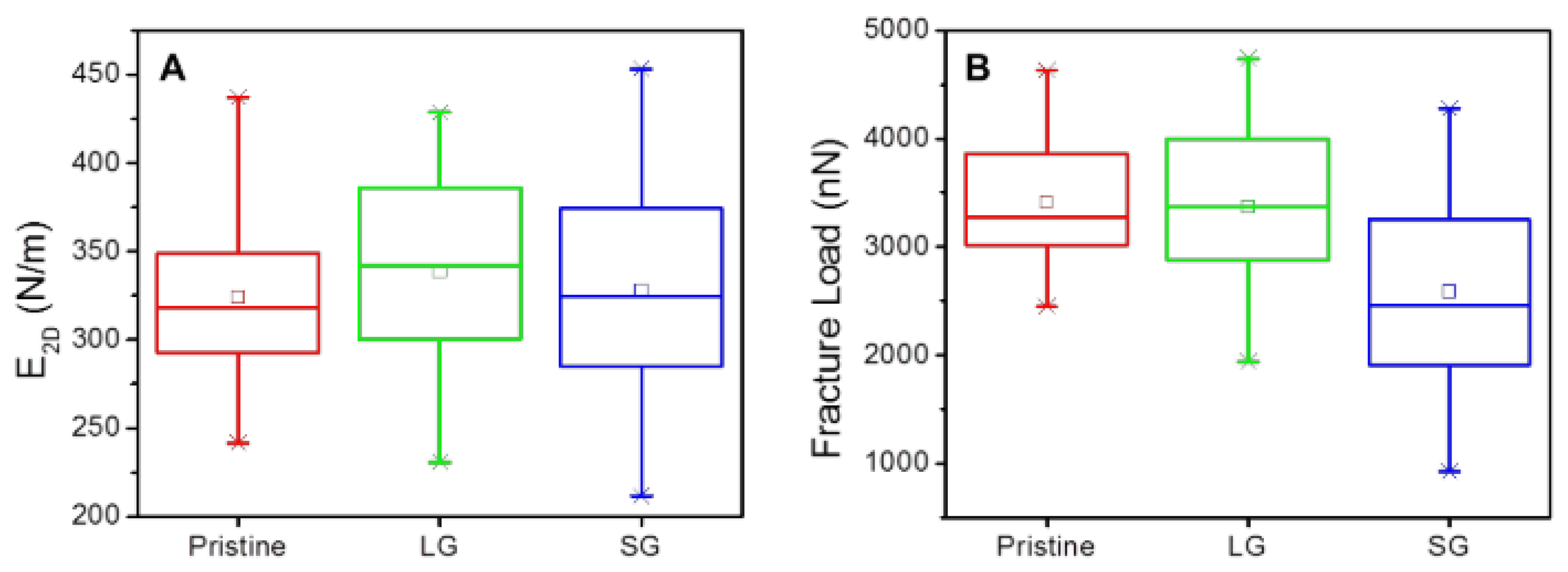
- Zandiatashbar, A.; Lee, G.H.; An, S.J.; Lee, S.; Mathew, N.; Terrones, M.; Hayashi, T.; Picu, C.R.; Hone, J.; Koratkar, N. Effect of defects on the intrinsic strength and stiffness of graphene. Nat. Commun. 2014, 5, 3186. [Google Scholar] [CrossRef]
- Ago, H.; Ogawa, Y.; Tsuji, M.; Mizuno, S.; Hibino, H. Catalytic Growth of Graphene: Toward Large-Area Single-Crystalline Graphene. J. Phys. Chem. Lett. 2012, 3, 2228–2236. [Google Scholar] [CrossRef]
- Ni, G.X.; Zheng, Y.; Bae, S.; Kim, H.R.; Pachoud, A.; Kim, Y.S.; Tan, C.L.; Im, D.; Ahn, J.H.; Hong, B.H.; et al. Quasi-Periodic Nanoripples in Graphene Grown by Chemical Vapor Deposition and Its Impact on Charge Transport. ACS Nano 2012, 6, 1158–1164. [Google Scholar] [CrossRef] [Green Version]
- Hummers, W.S.; Offeman, R.E. Preparation of Graphitic Oxide. J. Am. Chem. Soc. 1958, 80, 1339. [Google Scholar] [CrossRef]
- Dave, S.H.; Gong, C.; Robertson, A.W.; Warner, J.H.; Grossman, J.C. Chemistry and Structure of Graphene Oxide via Direct Imaging. ACS Nano 2016, 10, 7515–7522. [Google Scholar] [CrossRef]
- Cao, C.; Howe, J.Y.; Perovic, D.; Filleter, T.; Sun, Y. In situ TEM tensile testing of carbon-linked graphene oxide nanosheets using a MEMS device. Nanotechnology 2016, 27, 28LT01. [Google Scholar] [CrossRef] [PubMed]
- Robinson, J.T.; Zalalutdinov, M.; Baldwin, J.W.; Snow, E.S.; Wei, Z.; Sheehan, P.; Houston, B.H. Wafer-scale reduced graphene oxide films for nanomechanical devices. Nano Lett. 2008, 8, 3441–3445. [Google Scholar] [CrossRef] [PubMed]
- Patil, N.; Gupta, A.; Jaiswal, M.; Dutta, S. Chemical-free transfer of patterned reduced graphene oxide thin films for large area flexible electronics and nanoelectromechanical systems. Nanotechnology 2020, 31, 495301. [Google Scholar] [CrossRef] [PubMed]
- Restaino, M.; Eckman, N.; Alsharhan, A.T.; Lamont, A.C.; Anderson, J.; Weinstein, D.; Hall, A.; Sochol, R.D. In Situ Direct Laser Writing of 3D Graphene-Laden Microstructures. Adv. Mater. Technol. 2021, 6, 2100222. [Google Scholar] [CrossRef]


| Manufacturing Method | Number of Layers | E (GPa) | (GPa) | Ref. |
|---|---|---|---|---|
| Exfoliation | 23–43 | 1000 | - | [84] |
| Exfoliation | 1 | 1000 | 130 | [1] |
| Exfoliation | 1 | 1026 ± 22 | 125 ± 0 | [129] |
| Exfoliation | 2 | 962 ± 24 | 107.7 ± 4.3 | [129] |
| Exfoliation | 3 | 980 ± 10 | 105.6 ± 6.0 | [129] |
| Exfoliation | 8 | 942 ± 3 | 85.3 ± 5.4 | [129] |
| CVD on Cu | 1 | 160 | 35 | [130] |
| CVD on Cu (single grain) | 1 | - | 90–94 | [131] |
| CVD on Cu (poly-crystalline) | 1 | - | 53–77 | [131] |
| CVD on Cu | 1 | 1000 ± 150 | 103–118 | [127] |
| CVD on Cu (poly-crystalline small grain) | 1 | 423–1000 | 11.8 | [128] |
| CVD on Cu (poly-crystalline medium grain) | 1 | 423–1000 | 18 | [128] |
| CVD on Cu (single grain) | 1 | 1000 | 45.4 ± 10.4 | [128] |
| CVD on Cu (poly-crystalline small grain) | 1 | 380 ± 80 | - | [132] |
| CVD on Cu (poly-crystalline medium grain) | 1 | 790 ± 130 | - | [132] |
| CVD on Cu (single grain) | 1 | 950 ± 120 | - | [132] |
| CVD on Cu | 1 | 423 | 28.7 | [133] |
| CVD on Cu | 2 | 435 | 31.5 | [133] |
Publisher’s Note: MDPI stays neutral with regard to jurisdictional claims in published maps and institutional affiliations. |
© 2021 by the authors. Licensee MDPI, Basel, Switzerland. This article is an open access article distributed under the terms and conditions of the Creative Commons Attribution (CC BY) license (https://creativecommons.org/licenses/by/4.0/).
Share and Cite
Cho, J.H.; Cayll, D.; Behera, D.; Cullinan, M. Towards Repeatable, Scalable Graphene Integrated Micro-Nano Electromechanical Systems (MEMS/NEMS). Micromachines 2022, 13, 27. https://doi.org/10.3390/mi13010027
Cho JH, Cayll D, Behera D, Cullinan M. Towards Repeatable, Scalable Graphene Integrated Micro-Nano Electromechanical Systems (MEMS/NEMS). Micromachines. 2022; 13(1):27. https://doi.org/10.3390/mi13010027
Chicago/Turabian StyleCho, Joon Hyong, David Cayll, Dipankar Behera, and Michael Cullinan. 2022. "Towards Repeatable, Scalable Graphene Integrated Micro-Nano Electromechanical Systems (MEMS/NEMS)" Micromachines 13, no. 1: 27. https://doi.org/10.3390/mi13010027
APA StyleCho, J. H., Cayll, D., Behera, D., & Cullinan, M. (2022). Towards Repeatable, Scalable Graphene Integrated Micro-Nano Electromechanical Systems (MEMS/NEMS). Micromachines, 13(1), 27. https://doi.org/10.3390/mi13010027