Article

Influence of Etching Trench on Keff2 of Film Bulk Acoustic Resonator

1
The Institute of Technological Sciences, Wuhan University, Wuhan 430072, China
2
Hubei Yangtze Memory Laboratories, Wuhan 430072, China
*
Authors to whom correspondence should be addressed.
Micromachines 2022, 13(1), 102; https://doi.org/10.3390/mi13010102
Submission received: 18 December 2021 / Revised: 2 January 2022 / Accepted: 6 January 2022 / Published: 8 January 2022
(This article belongs to the Special Issue Recent Advances in RF MEMS)

Abstract

:
As radio-frequency (RF) communication becomes more ubiquitous globally, film bulk acoustic resonators (FBAR) have attracted great attention for their superior performance. One of the key parameters of an FBAR, the effective electromechanical coupling coefficient ( K e f f 2 ), has a great influence on the bandwidth of RF filters. In this work, we propose a feasible method to tune the K e f f 2 of the FBAR by etching the piezoelectric material to form a trench around the active area of the FBAR. The influence of the position of the etching trench on the K e f f 2 of the FBAR was investigated by 3D finite element modeling and experimental fabricating. Meanwhile, a theoretical electrical model was presented to test and verify the simulated and measured results. The K e f f 2 of the FBAR tended to be reduced when the distance between the edge of the top electrode and the edge of the trench was increased, but the Q value of the FBAR was not degraded. This work provides a new possibility for tuning the K e f f 2 of resonators to meet the requirements of different filter bandwidths.

1. Introduction

The rapid development of wireless mobile communication has led to higher requirements for radio-frequency (RF) devices. As an important element in the RF front-end, filters ideally possess large bandwidths, have low insertion losses and can undergo miniaturization [1]. Film bulk acoustic filters have been attracting researchers’ attention in recent years, since the achievable high acoustic velocity, good temperature stability and large electromechanical coupling coefficients ( K 2 ) of piezoelectric film materials, for example, aluminum nitride (AlN) and scandium-doped AlN (ScAlN), render them suitable to meet the harsh requirements of 5G wireless communication [2].
The effective electromechanical coupling coefficient ( K e f f 2 ) of a film bulk acoustic resonator (FBAR) is a core parameter which influences the bandwidth and cutoff frequency of filters. An adequate K e f f 2 bringing in a large bandwidth is achievable by using suitable piezoelectric materials or doping methods which are commonly used in previous process technologies. J.-S. Moulet et al. reported BAW devices fabricated with thin single crystalline LiNbO3 films and realized a K e f f 2 greater than 30% [3]. M. Pijolat et al. demonstrated that the K e f f 2 of LiNbO3-based FBAR can be as high as 43% [4,5]. Milena Moreira et al. illustrated that the K e f f 2 of ScAlN-based FBAR showed a linear two-fold increase when the Sc concentration was increased from 0 to 0.15 [6]. It is reported that the piezoelectric coefficient can be increased by about five times when the proportion of scandium doped in aluminum nitride is 40% [7,8,9,10,11]. However, manipulating the cutoff points to better satisfy the demand of the frequency band is challenging, and needs the precise control of the K e f f 2 of the FBAR. Researchers have indicated that changing the thickness ratio of the electrode and piezoelectric material can affect the K e f f 2 of an FBAR. K.M. Lakin et al. reported that the K e f f 2 of an FBAR was equal to the K 2 of the piezoelectric material when the electrode thickness was zero, and reached a maximum of 6.5% when the thickness ratio of the electrode to piezoelectric material was about 0.1 [12]. Hao Zhang et al. demonstrated that the K e f f 2 was reduced from 6.9% to 5.0% when the thickness of Mo(top)/AlN/Mo(bottom) was changed from 0.28 μm/1.18 μm/0.28 μm to 0.46 μm/0.62 μm/0.46 μm, since the conversion efficiency between electrical energy and sound energy was reduced [13]. However, precise thickness control is difficult in actual processing. Adding external passive devices such as capacitors and inductors into circuits can also influence the K e f f 2 of an FBAR. Qingrui Yang et al. indicated that the 3 dB bandwidth of an AlN-based bulk acoustic wave (BAW) filter can be up to 12.3% under the influence of adding auxiliary inductors to the lattice topology, which was more than twice that of the conventional AlN-based BAW filter [14]. Paras Chawla et al. indicated that the introduction of inductors in the filter topology increased the bandwidth of a BAW filter, while the introduction of capacitors did the opposite and reduced the bandwidth of the filter [15]. However, the introduction of passive devices has a great impact on the Q value of the resonator and causes an increase in the filter volume.
In this paper, the piezoelectric material was etched to form a trench around the active area of resonators and the trench can be equivalent to an external capacitor. The value of the external capacitor was adjusted by changing the position of the etching trench. The influence of the etching trench on the K e f f 2 of the FBAR was investigated by using the finite element method (FEM) and FBAR devices with different trench positions were also manufactured for further verification. Both the simulated and measured results indicated that the K e f f 2 of the FBAR decreased as the distance (d) between the trench and the edge of the electrode increased; the measured K e f f 2 was 18.3% when d was 0 but dropped to 14.6% when d was 12 μm. Additionally, the Q value of the FBAR was calculated and normalized; the results show that it nearly remained unchanged. We have proved that the etching trench can indeed tune the K e f f 2 of the FBAR without degenerating the Q value of the FBAR. The K e f f 2 of the FBAR can be well adjusted with the etching trench in the fabricating process, which can be potentially used in future work.

2. Materials and Methods

Figure 1a shows the cross-sectional view of the FBAR with the etched trench; the region where the top and bottom electrodes overlap with the piezoelectric material is the active area of the FBAR. The introduction of the trench can be equivalent to a parallel capacitor ( C p ) connecting with the resonator.
For FBAR devices, the K e f f 2 is calculated as [16]:
K e f f 2 = π 2 4 f s f p f p f s f p ,
where f s and f p are the series and parallel resonant frequencies, respectively. The MBVD (Modified Butterworth–Van Dyke) model [17], as shown in Figure 1b, can be used to express the electric characteristics of the FBAR. The model consists of six elements: C 0 is the static capacitance, C m is the motional capacitance, and L m is the motional inductance. The remaining parameters R m , R s and R 0 represent the motional resistance, electrode ohmic loss parasitic and acoustic loss parasitic, respectively. The series R m - C m - L m circuit branch reflects the interaction between the RF (radio-frequency) signal and the bulk acoustic wave. The series frequency of the FBAR can be expressed in terms of L m and C m , and the shunt frequency of the FBAR can be expressed in terms of L m , C m and R m . The calculations of f s and f p are as follows [18]:
f s = 1 2 π L m C m ,
f p = 1 2 π C m + C 0 C m C 0 L m = f s C m C 0 + 1 ,
As shown in Figure 1c, we proposed an MBVD model with the external parallel capacitor to describe the electric characteristic of the FBAR with the etching trench shown in Figure 1a. Using the MBVD model, we found that f s remains unchanged and f p can be expressed as:
f p = 1 2 π C m + C 0 + C p C m L m ( C 0 + C p ) = f s C m C 0 + C p + 1 ,
According to Formulas (1), (2) and (4), the K e f f 2 of the FBAR can be tuned by changing C p .
A 3D finite element model was built in finite element simulation software COMSOL Multiphysics to simulate the influence of the etching trench on the performance of the FBAR. Figure 2a,b show the 3D cross-sectional schematics of the traditional FBAR and the FBAR with the etching trench, respectively. The difference between these two types of resonators is that the piezoelectric material of the latter is etched to form a trench for changing the K e f f 2 of the resonator. The distance d between the edge of the trench and the edge of the top electrode was set to values of 0 μm, 2 μm, 4 μm, 8 μm and 12 μm, to change the value of C p , but the width of the trench remained constant at 2 μm. The FBAR structure of the 3D model was a layer stack of seed Ti layer, bottom Mo electrode, middle Sc0.20Al0.80N piezoelectric layer and top Mo electrode. The thicknesses of the piezoelectric film, the bottom/top electrode and the seed layer were 580 nm, 50 nm and 20 nm, respectively.
We also fabricated the FBAR devices to test and verify the simulated results. Each layer of the resonator was processed to the same thickness as the 3D simulation model, and the distance d was processed to a variable from 0 to 12 μm, while the width of the trench was processed to the same fixed value of 2 μm as per the 3D simulation model defined. Figure 2c,d show the top and cross-sectional SEM images of the resonator with the etching trench, respectively. Figure 2e shows the energy-dispersive spectroscopy (EDS) elemental results of the devices; the atomic percent indicates that the scandium-doping ratio was 20%.
The detailed fabrication process is illustrated in Figure 3. The fabrication process started with etching a silicon substrate to form a swimming pool which functioned as an air reflection interface of bulk acoustic waves. Then, silicon dioxide (SiO2) was deposited on the substrate as a sacrificial layer to fill the entire air cavity by low-pressure chemical vapor deposition (LPCVD). Chemical–mechanical polishing (CMP) stopping on silicon was used to remove superfluous SiO2. Next, a 20 nm-thick seed Ti layer was deposited to obtain a piezoelectric film with better quality, and a 50 nm-thick bottom Mo electrode was deposited and patterned. Then, 580 nm-thick Sc0.20Al0.80N was deposited by magnetron sputtering, and the ScAlN thin film was etched by inductively coupled plasma (ICP) dry etch with an etching rate of 90 nm/min, so that connecting holes were formed. After that, a 50 nm-thick top Mo electrode was deposited and patterned. Subsequently, a 1 μm-thick Al electrode was deposited and patterned to serve as the electrode pad. Finally, release holes and trench were formed by etching the ScAlN again, and VHF (vapor hydrofluoric acid) dry etching was used to etch the SiO2 in the swimming pool, thus releasing the whole FBAR device.

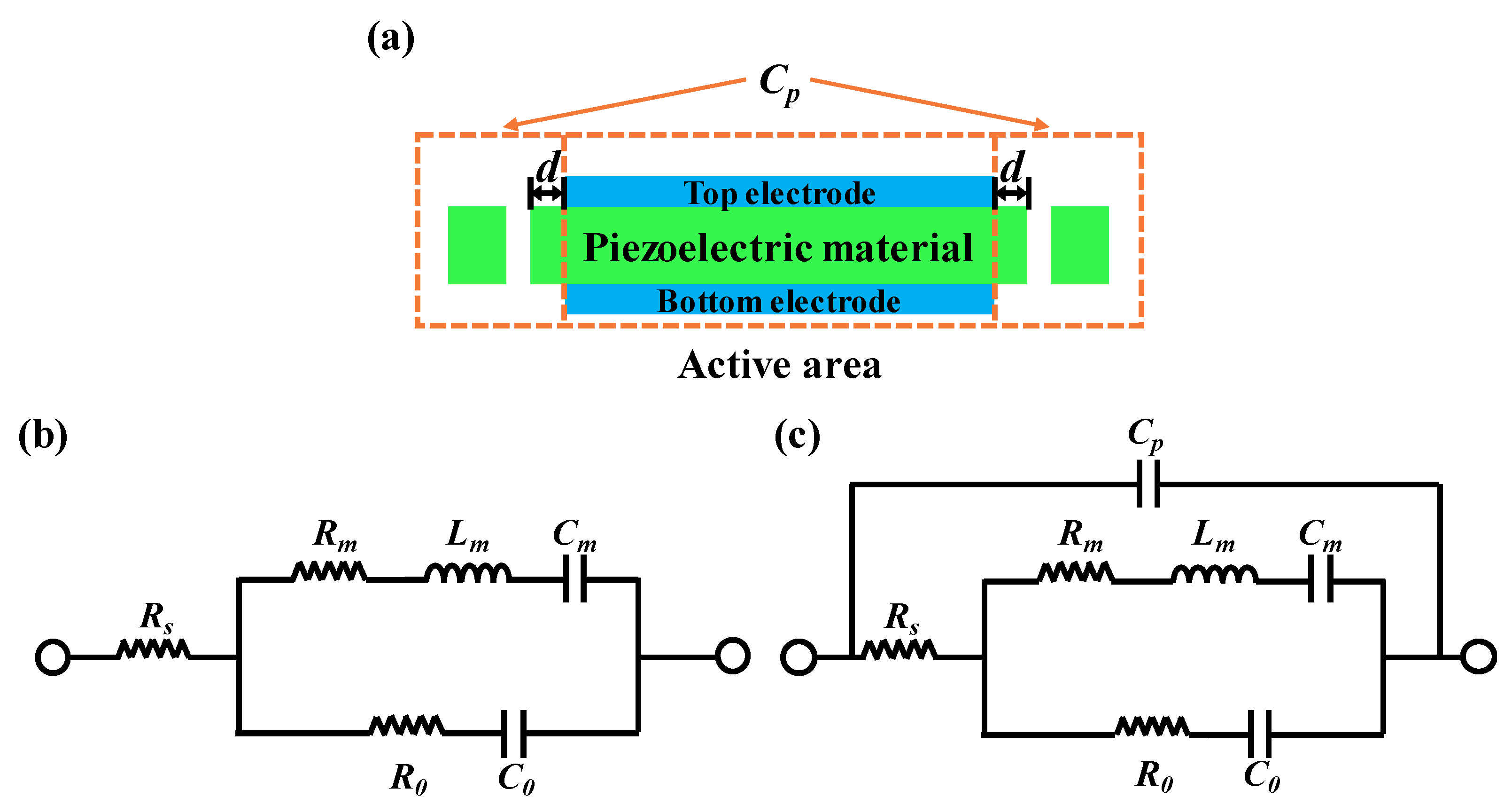
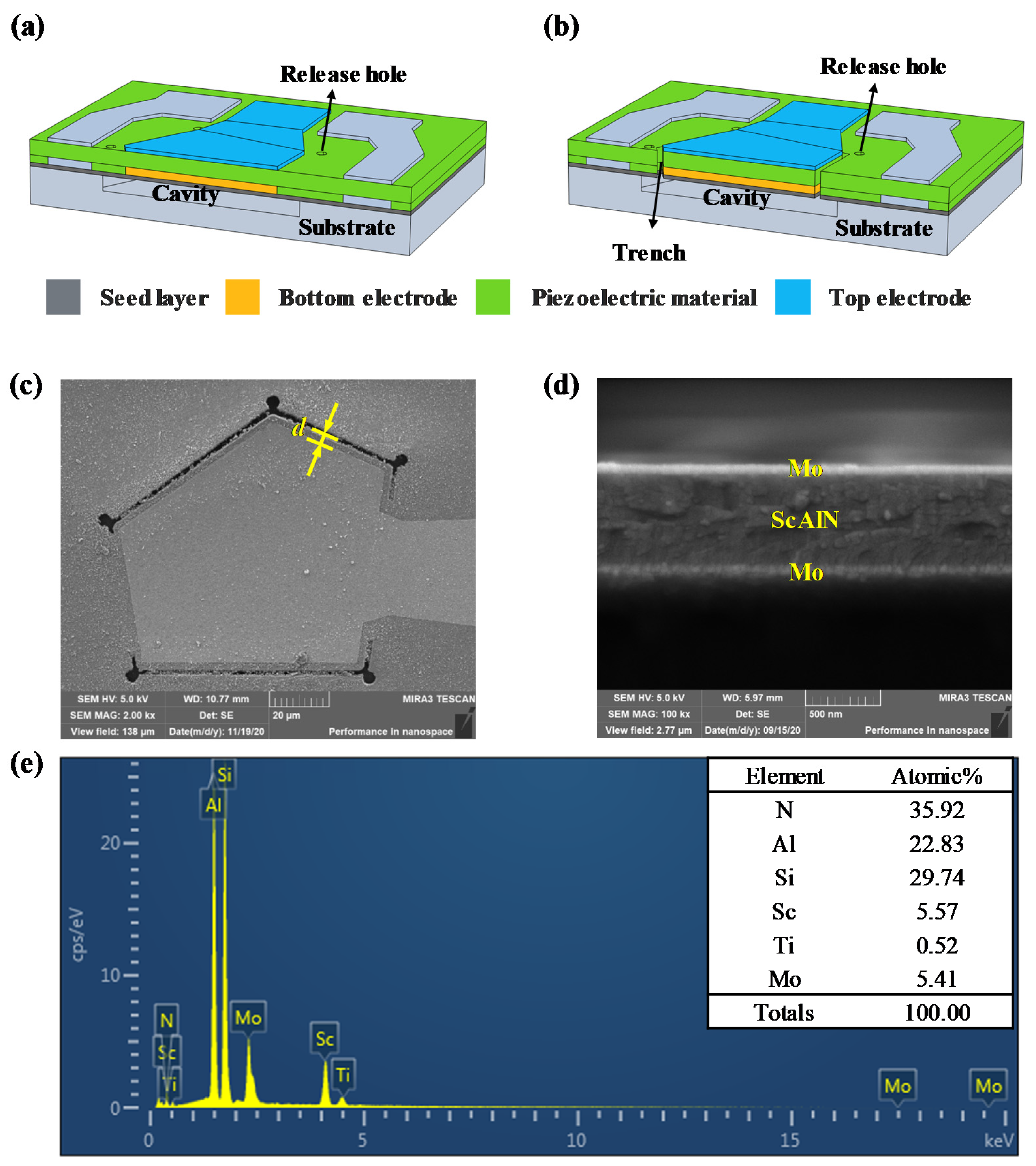
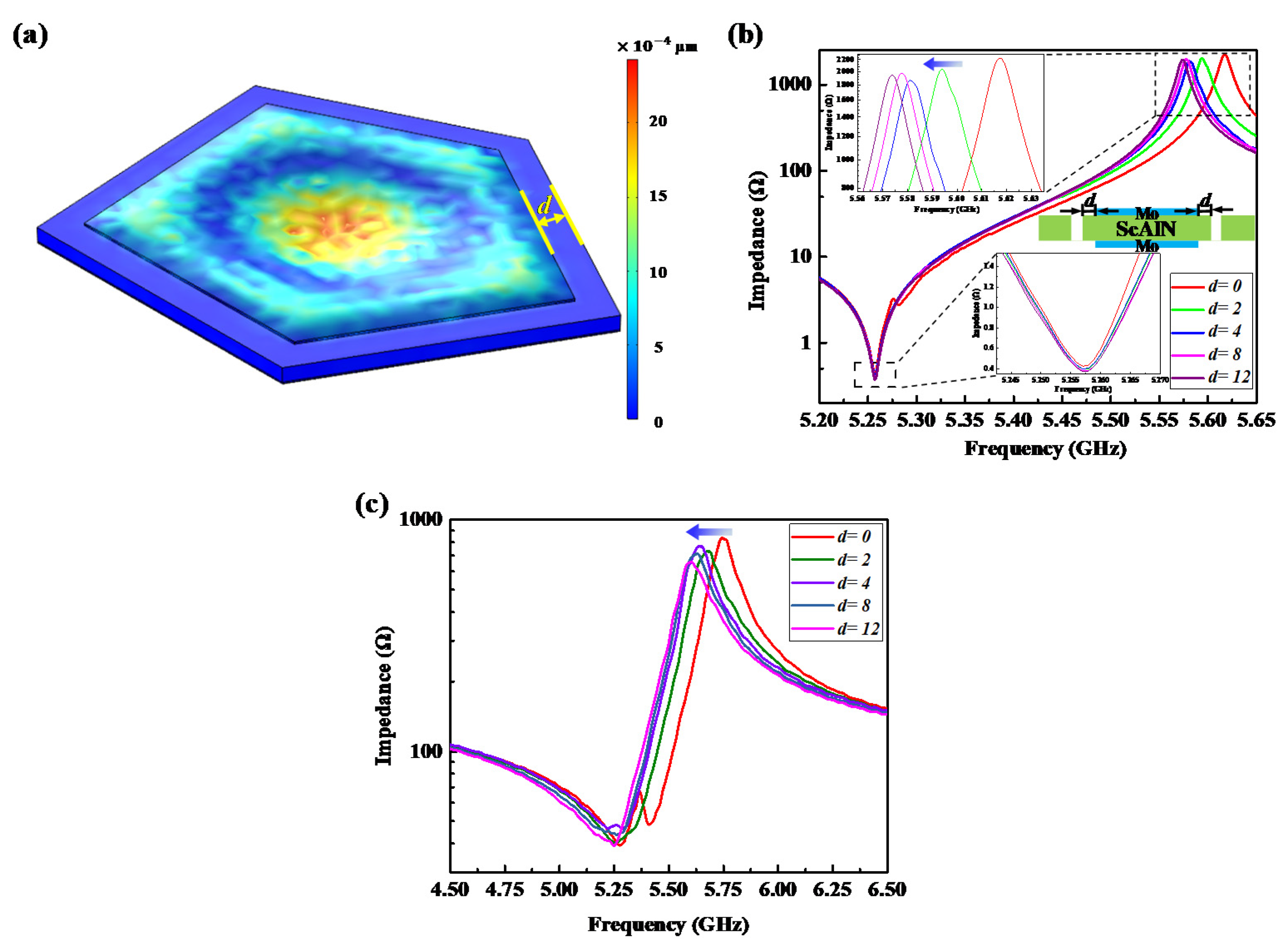
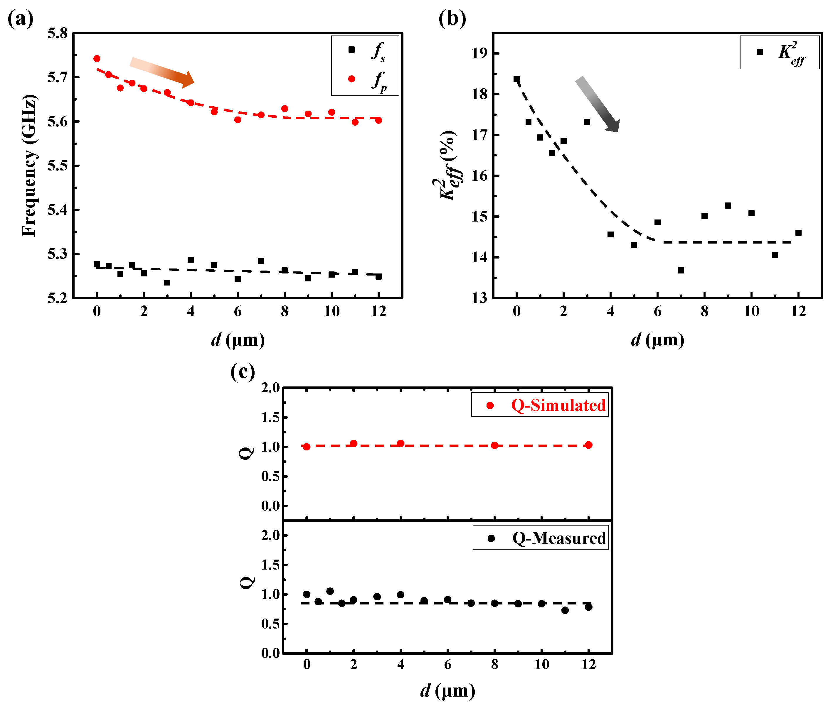
3. Results and Discussion

The displacement shape at resonant frequency is shown in Figure 4a; it is the thickness vibration mode. The simulated frequency response of the FBAR at different distances d is presented in Figure 4b; the distance d was set to 0, 2 μm, 4 μm, 8 μm or 12 μm. As shown in Figure 4b, the series resonant frequency of the FBAR was 5.257 GHz and the shunt resonant frequency was at 5.617 GHz when d was 0. As the distance d increased, all the series resonant frequencies of the FBARs were still at 5.527 GHz, but the parallel resonant frequencies became smaller. The measured frequency responses presented in Figure 4c also prove the same influence of distance d on the position of the resonant frequency.
The detailed frequency change of the measured results can be seen in Figure 5a. f s remained almost unchanged, and f p dropped slowly first and tended to become a constant with the distance d increased. Figure 5b shows the tendency of the calculated K e f f 2 by Formula (1); K e f f 2 was 18.3% when d was 0 and decreased to 14.6% when d was 12 μm. Compared with the electrical loss, the loss caused by the etching trench can be very small; therefore, the influence of the etching trench on the Q factor will be relatively small. Figure 5c demonstrates the variation rule of the normalized Bode-Q [19] value of the simulated and measured results. Both the simulated and measured results note the same trend that the Q value remained unchanged when d was increased, which means the influence of the etching trench on the Q value of the FBAR can be ignored.
Figure 6a shows that f p was reduced but f s remained unchanged when an external capacitor was in parallel with the resonator. As shown in Figure 6b, the measured resonance frequencies with d equal to 0, 1.5 μm or 5 μm, can be well fitted by the MBVD model with different external C p . Generally, the variation of distance d can be regarded as equivalent to the alteration of external C p .

4. Conclusions

In this work, we proposed using etching piezoelectric material to form a trench near the active area of an FBAR to tune K e f f 2 . The influence of the etching trench on the FBAR was investigated using FEM and fabricating resonators with the etching trench located at different positions. The parallel resonant frequency and K e f f 2 of the resonator were influenced by the etching trench position and decreased as the distance d increased, but the effects of the etching trench position on the series resonant frequency and the Q value were negligible. We also theoretically proposed a modified electrical model to verify the simulated and measured results; the introduction of the etching trench can be equivalent to an external C p connection with the resonator. Using Sc0.20Al0.80N as the piezoelectric functional material, an FBAR with adjustable K e f f 2 of 14% to 18.3%, controlled by the position of the etching trench, was obtained. The proposed etching trench in piezoelectric materials can be compatibly achieved in the fabrication process and provides a potential solution for finely adjusting the bandwidth of filters in the future.

Author Contributions

Conceptualization, C.S. and Y.C.; methodology, C.G., J.Z. and W.L.; writing—original draft preparation, C.G. and Y.Z.; writing—review and editing, C.G., Y.C. and Y.L.; supervision, C.S. All authors have read and agreed to the published version of the manuscript.

Funding

This work was supported by the National Key R&D Program of China (Grant No. 2020YFB2008803).

Institutional Review Board Statement

Not applicable.

Data Availability Statement

Data is contained within the article.

Conflicts of Interest

The authors declare no conflict of interest.

References

  1. Bi, F.Z.; Barber, B.P. Bulk acoustic wave RF technology. IEEE Microw. Mag. 2008, 9, 65–80. [Google Scholar] [CrossRef]
  2. Hashimoto, K.-Y. Rf Bulk Acoustic Wave Filters for Communications; Artech House: Norwood, MA, USA, 2009. [Google Scholar]
  3. Moulet, J.-S.; Pijolat, M.; Dechamp, J.; Mazen, F.; Tauzin, A.; Rieutord, F.; Reinhardt, A.; Defay, E.; Deguet, C.; Ghyselen, B. High piezoelectric properties in LiNbO3 transferred layer by the Smart Cut™ technology for ultra wide band BAW filter applications. In Proceedings of the 2008 IEEE International Electron Devices Meeting, San Francisco, CA, USA, 15–17 December 2008; pp. 1–4. [Google Scholar]
  4. Pijolat, M.; Loubriat, S.; Queste, S.; Mercier, D.; Reinhardt, A.; Defaÿ, E.; Deguet, C.; Clavelier, L.; Moriceau, H.; Aid, M. Large electromechanical coupling factor film bulk acoustic resonator with X-cut LiNbO3 layer transfer. Appl. Phys. Lett. 2009, 95, 182106. [Google Scholar] [CrossRef]
  5. Pijolat, M.; Loubriat, S.; Mercier, D.; Reinhardt, A.; Defaÿ, E.; Deguet, C.; Aïd, M.; Queste, S.; Ballandras, S. LiNbO3 film bulk acoustic resonator. In Proceedings of the 2010 IEEE International Frequency Control Symposium, Newport Beach, CA, USA, 1–4 June 2010; pp. 661–664. [Google Scholar]
  6. Moreira, M.; Bjurström, J.; Katardjev, I.; Yantchev, V. Aluminum scandium nitride thin-film bulk acoustic resonators for wide band applications. Vacuum 2011, 86, 23–26. [Google Scholar] [CrossRef]
  7. Konno, A.; Sumisaka, M.; Teshigahara, A.; Kano, K.; Hashimo, K.-Y.; Hirano, H.; Esashi, M.; Kadota, M.; Tanaka, S. ScAlN Lamb wave resonator in GHz range released by XeF2 etching. In Proceedings of the 2013 IEEE International Ultrasonics Symposium (IUS), Prague, Czech Republic, 21–25 July 2013; pp. 1378–1381. [Google Scholar]
  8. Akiyama, M.; Kamohara, T.; Kano, K.; Teshigahara, A.; Takeuchi, Y.; Kawahara, N. Enhancement of piezoelectric response in scandium aluminum nitride alloy thin films prepared by dual reactive cosputtering. Adv. Mater. 2009, 21, 593–596. [Google Scholar] [CrossRef] [PubMed]
  9. Parsapour, F.; Pashchenko, V.; Chambon, H.; Nicolay, P.; Bleyl, I.; Roesler, U.; Muralt, P. Free standing and solidly mounted Lamb wave resonators based on Al0.85Sc0.15N thin film. Appl. Phys. Lett. 2019, 114, 223103. [Google Scholar] [CrossRef]
  10. Colombo, L.; Kochhar, A.; Xu, C.; Piazza, G.; Mishin, S.; Oshmyansky, Y. Investigation of 20% scandium-doped aluminum nitride films for MEMS laterally vibrating resonators. In Proceedings of the 2017 IEEE International Ultrasonics Symposium (IUS), Washington, DC, USA, 6–9 September 2017; pp. 1–4. [Google Scholar]
  11. Akiyama, M.; Kano, K.; Teshigahara, A. Influence of growth temperature and scandium concentration on piezoelectric response of scandium aluminum nitride alloy thin films. Appl. Phys. Lett. 2009, 95, 162107. [Google Scholar] [CrossRef]
  12. Lakin, K.M.; Belsick, J.; McDonald, J.; McCarron, K. Improved bulk wave resonator coupling coefficient for wide bandwidth filters. In 2001 IEEE Ultrasonics Symposium. Proceedings. An International Symposium (Cat. No. 01CH37263), Proceedings of the 2001 IEEE Ultrasonics Symposium, Atlanta, GA, USA, 7–10 October 2001; IEEE: Piscataway, NJ, USA, 2001; pp. 827–831. [Google Scholar]
  13. Zhang, H.; Pang, W.; Chen, W.; Zhou, C. Design of unbalanced and balanced radio frequency bulk acoustic wave filters for TD-SCDMA. In Proceedings of the 2010 International Conference on Microwave and Millimeter Wave Technology, Chengdu, China, 8–11 May 2010; pp. 878–881. [Google Scholar]
  14. Yang, Q.; Pang, W.; Zhang, D.; Zhang, H. A modified lattice configuration design for compact wideband bulk acoustic wave filter applications. Micromachines 2016, 7, 133. [Google Scholar] [CrossRef] [PubMed] [Green Version]
  15. Chawla, P.; Garg, A.; Singh, S. A high performance multiband BAW filter. Int. J. Inf. Technol. 2019, 11, 779–783. [Google Scholar] [CrossRef]
  16. Lakin, K.M.; Kline, G.R.; McCarron, K.T. High-Q microwave acoustic resonators and filters. IEEE Trans. Microw. Theory Tech. 1993, 41, 2139–2146. [Google Scholar] [CrossRef]
  17. Larson, J.D.; Bradley, P.D.; Wartenberg, S.; Ruby, R.C. Modified Butterworth-Van Dyke circuit for FBAR resonators and automated measurement system. In 2000 IEEE Ultrasonics Symposium. Proceedings. An International Symposium (Cat. No. 00CH37121), Proceedings of the 2000 IEEE Ultrasonics Symposium, San Juan, PR, USA, 22–25 October 2000; IEEE: Piscataway, NJ, USA, 2000; pp. 863–868. [Google Scholar]
  18. Bjurstrom, J.; Vestling, L.; Olsson, J.; Katardjiev, I. An accurate direct extraction technique for the MBVD resonator model. In Proceedings of the 34th European Microwave Conference, Amsterdam, The Netherlands, 12–14 October 2004; pp. 1241–1244. [Google Scholar]
  19. Feld, D.A.; Parker, R.; Ruby, R.; Bradley, P.; Dong, S. After 60 years: A new formula for computing quality factor is warranted. In Proceedings of the 2008 IEEE Ultrasonics Symposium, Beijing, China, 2–5 November 2008; pp. 431–436. [Google Scholar]
Figure 1. (a) Cross-sectional structure of FBAR with the etching trench. (b) The MBVD model of FBAR without C p . (c) The MBVD model with C p .
Micromachines 13 00102 g001
Figure 2. 3D cross-sectional schematics: (a) Traditional FBAR and (b) FBAR with trench. Scanning electron microscope (SEM) images for the fabricated FBAR: (c) Top view of FBAR with trench. (d) Cross-sectional view of FBAR with trench. (e) Energy-dispersive spectroscopy (EDS) elemental spectrum and quantification results.
Micromachines 13 00102 g002
Figure 3. ScAlN FBAR fabrication process flow diagram: (a) Etching swimming pool on high-resistance silicon. (b) Deposit SiO2 and CMP. (c) Deposit Ti and Mo, pattern. (d) Deposit ScAlN, pattern. (e) Deposit Mo, pattern. (f) Deposit Al pad, pattern. (g) Etch release holes and trench. (h) VHF release SiO2.
Micromachines 13 00102 g003
Figure 4. (a) The displacement shape at resonant frequency. Impedance curves of FBARs with the distance d changed: (b) Simulated results. (c) Measured results.
Micromachines 13 00102 g004
Figure 5. (a) The detailed frequency change of measured results with different distance d. (b) The calculated K e f f 2 . (c) The normalized Q values of FBARs with different distances d.
Micromachines 13 00102 g005
Figure 6. (a) Comparison of impedance curves with and without an external capacitor connected in parallel with a resonator. (b) Measured frequencies of resonators with different distance (d) are fitted by capacitors ( C p ).
Micromachines 13 00102 g006
Publisher’s Note: MDPI stays neutral with regard to jurisdictional claims in published maps and institutional affiliations.

