1. Introduction
NAND flash memories have been widely used in smartphones, personal computers, data centers, etc. Thanks to these two key technologies: (1) continued scaling down process technology and (2) multilevel (e.g., MLC, TLC) cell data coding, the storage density of a NAND flash memory has been significantly increased over previous decades [
1]. However, these two key technologies bring about a challenge in that the data stored in NAND flash memory may suffer from low reliability [
2,
3,
4]. Furthermore, there are two major sources of noise in flash memory: cell-to-cell interference (CCI) and retention noise. Numerous works have been proposed to mitigate noises in NAND flash memory. For example, the data post compensation and predistortion technique [
5] and detector design using a neighbor-a-priori information technique [
6] exploit the a-priori information of the neighboring cells to mitigate the CCI. However, when considering retention noise, the voltage offset of flash memory cell tends to become unknown. It may be hard to use the a-priori information of the neighboring cells to compensate for the voltage shift caused by CCI. In addition, the CCI removal technique proposed by Lin [
7] suffers from a similar problem in that the proposed technique ignores the impact of noise. In addition, Reference [
8] proposed a retention-aware belief-propagation (BP) decoding scheme to mitigate the retention noise effect but did not take CCI into consideration.
Against the above background, the recent advances in neural networks and machine learning provide a new perspective to increase the reliability of MLC NAND flash memory. The key idea of the neural network is to learn an optimal network model from the massive training data, instead of using a definitive algorithm that is derived from a pre-defined model [
9]. A pioneering work is reported in [
10,
11], which utilizes an artificial neural network to predict the threshold voltage distribution of NAND flash memory. In the pretesting, the above method assumes that the prior information of the retention time is informed in advance. When the flash controller is powered off, we cannot obtain the retention time.
In this paper, we use the neural network to learn an optimal network model to detect the bits errors in the cells that are disturbed by both CCI and retention noise and propose a neural network-assisted error correction scheme. However, it is difficult to record the retention time in a practical system, which means that accurate LLR values cannot be calculated. Therefore, we propose using relative LLR to estimate the actual LLR. The relative LLR is affected little by retention time, so we do not require retention time as an input parameter of the neural network.
In this paper, we first model the threshold voltage distribution as a Gaussian mixture model, which is fairly close to the voltage distribution of the practical NAND flash memory, and we calculate the LLR of the theoretical threshold distribution using a quantization scheme. Then, the corresponding LLR of the actual threshold distribution is mapped according to the relative position of the optimal reading reference voltage. It is found that this idea makes the relative LLR values remain relatively steady throughout retention time, which allows us to avoid using retention time as an input parameter of the neural network. Finally, using the relative LLR to estimate the actual LLR, we train the neural network and use the trained network to recovery the bits that may be wrongly detected in the soft-decision detection or hard-decision detection.
The rest of this paper is organized as follows. The flash channel model is presented in
Section 2.
Section 3 introduces our proposed ANNAEC scheme. Numerical simulation results are presented in
Section 4. The conclusions are drawn in
Section 5.
2. Channel Model
Without loss of generality, the proposed ANNAEC is performed over a model-based MLC NAND flash memory. Based on [
5,
8,
12], we can model threshold voltage,
, by
where
V denotes the desired voltage level,
denotes random telegraph noise (RTN),
denotes the shift caused by
CCI noise, and
denotes retention noise.
2.1. The Voltage Distribution of Programmed and Erased Cell
The number of charges in the NAND flash memory cell can be altered in the program and erase operation. It is well known that before being programmed, a flash memory cell must be erased. In the erase operation, the charges in the memory cell are removed from the floating gate, and the threshold voltage of the erased cell will be set to the lowest voltage. The threshold voltage distribution of an erased cell follows a Gaussian distribution, which is given by
where
and
are the standard deviation and the mean of the threshold voltage of the erased cell, respectively.
According to [
5,
8], the threshold voltage of a programmed cell follows a Gaussian distribution shown below:
where
and
are the standard deviation and the mean of the threshold voltage of a programmed cell.
2.2. RTN
The electron capture and emission at the floating gate near the interface generate RTN, which is greatly impacted by flash memory P/E cycles [
13]. As P/E cycles increase, the tunnel oxide of the floating gate transistor is gradually damaged and generates charge trapping in the oxide and interface states. RTN leads to a random fluctuation of cell threshold voltage and widens the voltage distribution. Hence, RTN is modeled with a Gaussian-like distribution [
8], given as
where
, denotes the noise standard deviation.
2.3. CCI
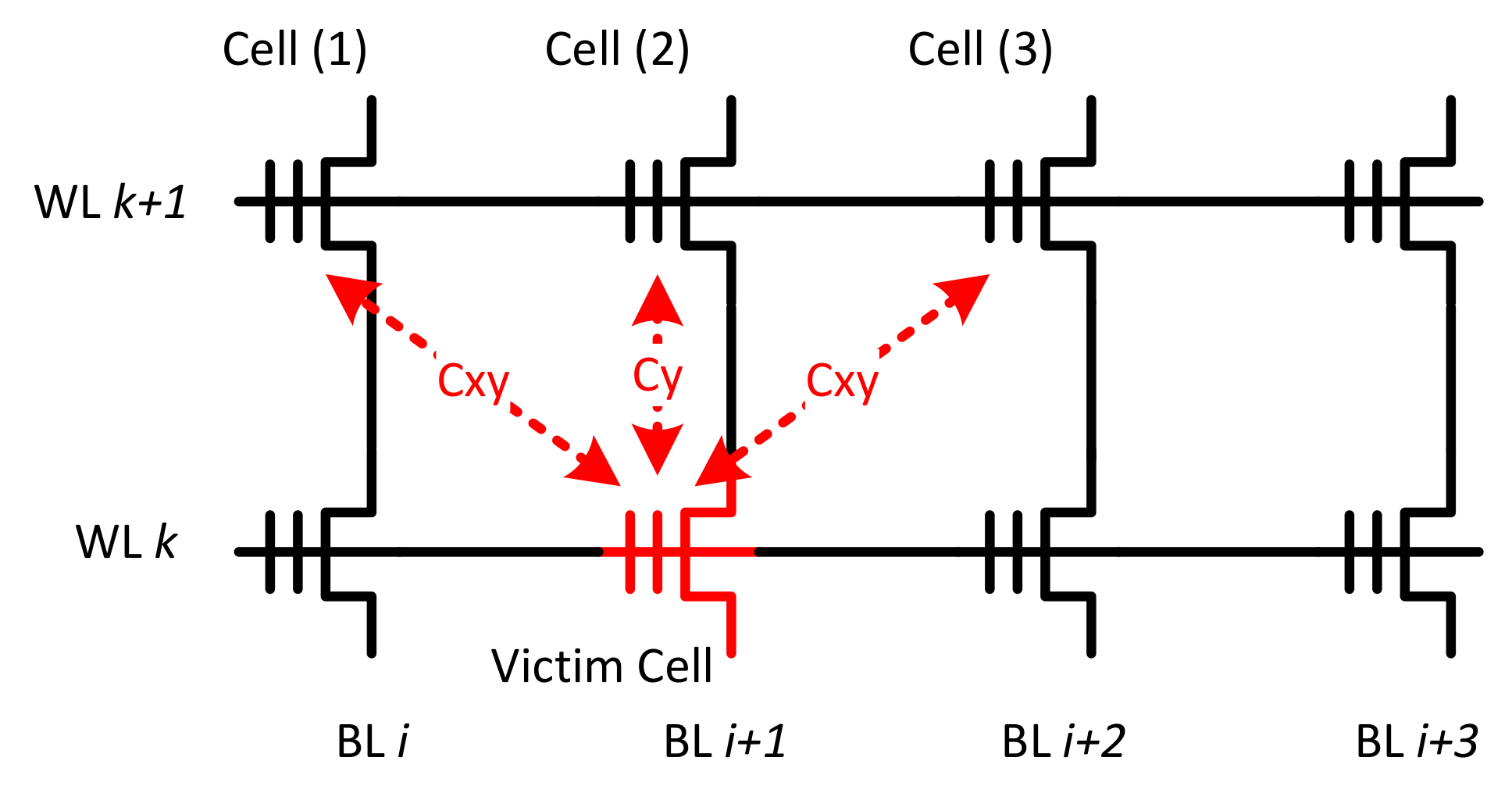
Because of the parasitic capacitance-coupling effect among adjacent cells in flash memory, the threshold voltage of the victim cell increases as the threshold voltage of an adjacent cell increases. The immediate adjacent cells are the major noise source of the CCI. We consider an all bit-line structure. As shown in
Figure 1, when the (
k+1)-th wordline (WL) has been programmed, the cell on the
k-th WL can be programmed. Hence, the victim cell is influenced by three immediate adjacent cells. The threshold-voltage shift of the victim cell can be modeled as a linear combination of the threshold voltage changes of those immediate adjacent cells. We can estimate the threshold-voltage shift caused by CCI as
where
is the change of an immediate adjacent cell, which is programmed after the victim cell and
represents the coupling ratio. We assume the vertical and the diagonal coupling ratio are
and
, respectively. According to the cell-to-cell coupling strength factor
s, we can set
and
[
12].
2.4. Retention
After a cell is programmed, the number of charges in the NAND flash memory cell continually reduce over time due to trap-assisted tunneling and charge detrapping [
1]. Retention noise is modeled as a Gaussian distribution, i.e.,
. The mean
, and the standard deviation
, are given by
where
is the cell voltage change before and after being programmed,
T donates memory retention time and
is the number of PE cycles.
The conditional probability distribution function of the threshold voltage after being disturbed by RTN, CCI and retention are given as follows:
where
,
and
are the means of cells 1–3, respectively, which are shown in
Figure 2,
and
are the mean and standard deviation of the victim cell.
In this paper, we set the flash memory parameters as follows: , , , , , , , , and .
3. Artificial Neural Network-Assisted Error Correction
In this section, we first present the idea of relative LLR calculation. Then we explain why an artificial neural network is useful for NAND flash memory. Finally, we introduce our proposed ANNAEC scheme.
3.1. Relative LLR
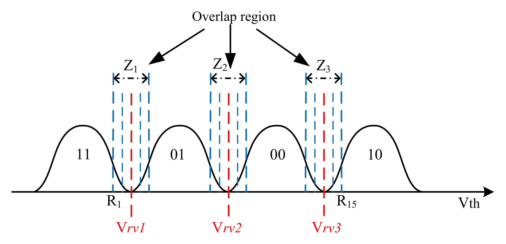
For soft decision belief-propagation (BP) decoding, a soft quantization scheme has been proposed. As an example,
Figure 2 shows a 15-level uniform sensing quantization [
12].
The overlap region is obtained by the entropy of the cell’s threshold voltage [
12,
14]. When the threshold voltage falls into the range
, where
is the
n-th reference voltage,
and
, the LLR values of the least significant bit (LSB) and the most significant bit (MSB) in the
i-th cell can be calculated by (
12) and (
13), respectively:
However, it may be hard to accurately calculate the LLR values due to the retention noise. Even though retention noise is modeled as Gaussian distribution, the mean and the standard deviation are random, since
is random as described in (
6) and (
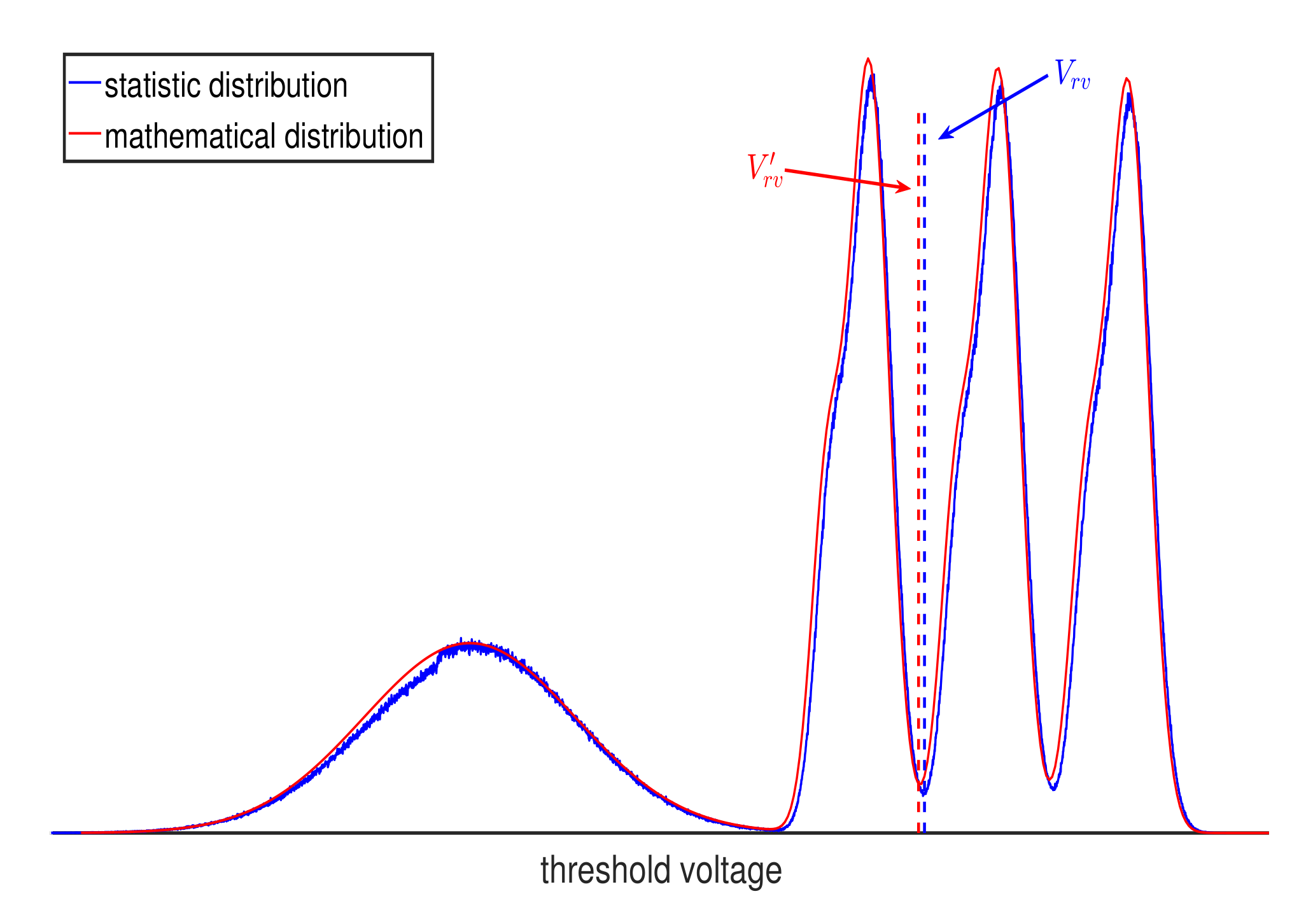
7). Furthermore, it is difficult to obtain accurate retention time in a practical system. To deal with those problems, we can estimate LLR, based on the relative reference voltage positions, given as
where
means that we estimate
in Equations (
6) and (
7) as
,
and
are the reference voltages of the actual threshold distribution and the theoretical threshold distribution, respectively, as shown in
Figure 3, where
is obtained by voltage optimization [
1] and
is obtained by theoretical calculations, such as minimizing entropy of the cell’s threshold voltage [
12,
14]. In (
14) and (
15), we first calculate the LLR of the theoretical threshold distribution using a quantization scheme. Then, the corresponding LLR of the actual threshold distribution is mapped according to the relative position of the optimal reference voltage.
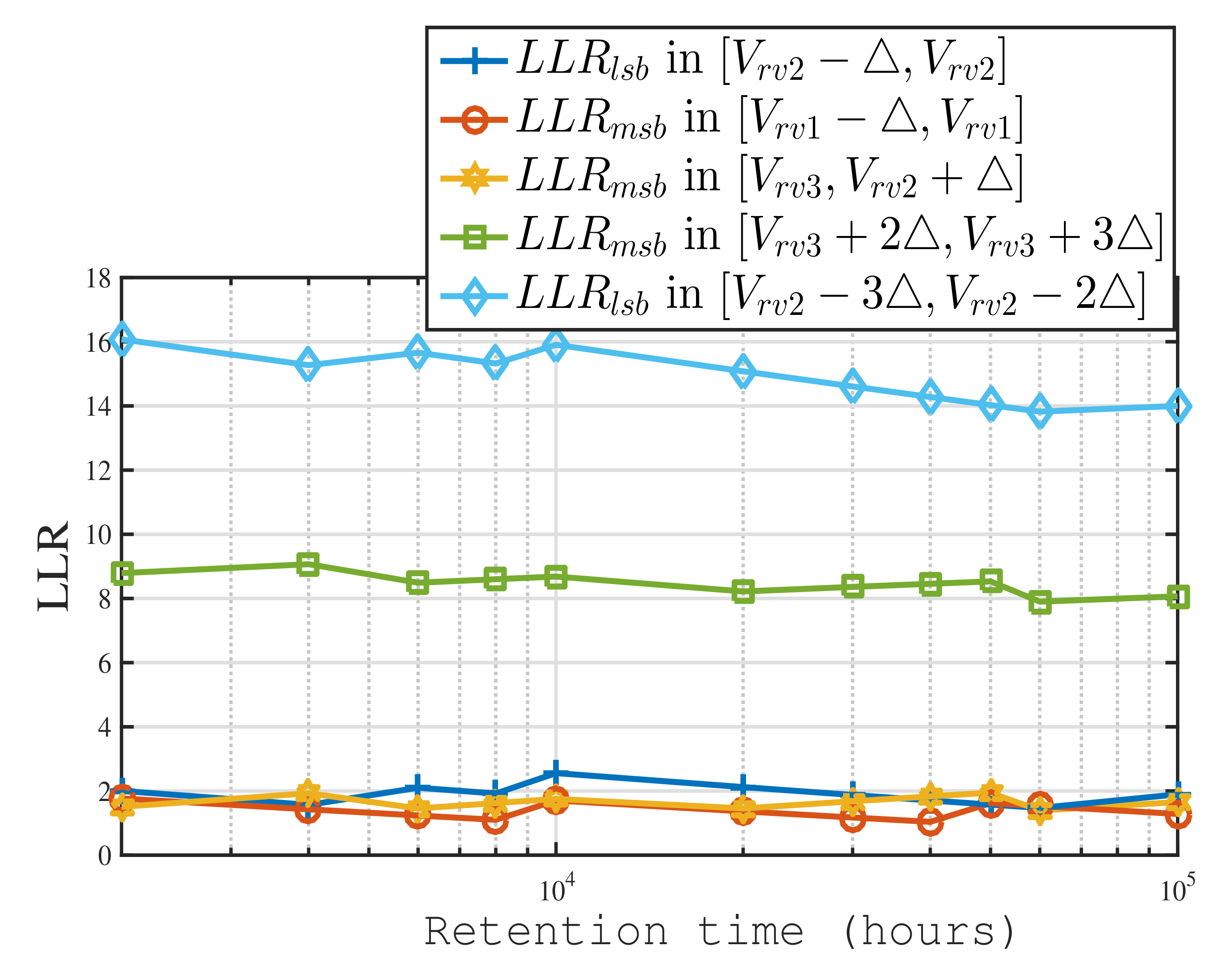
We depict the relative LLR versus data retention time in
Figure 4. The relative LLR values remain relatively steady, which allows the neural network to not require retention time as an input parameter. In addition, LLR calculation is offline in a flash memory controller [
15]. It may be difficult for a controller to estimate the characteristics of the memory channel because online estimation leads to a significant increase in the power consumption and read latency of the flash controller. Therefore, the proposed relative LLR can estimate the actual LLR over a time range, which can also help reduce the number of LLR tables stored in the controller.
3.2. Why Are Artificial Neural Networks Useful for NAND Flash Memory?
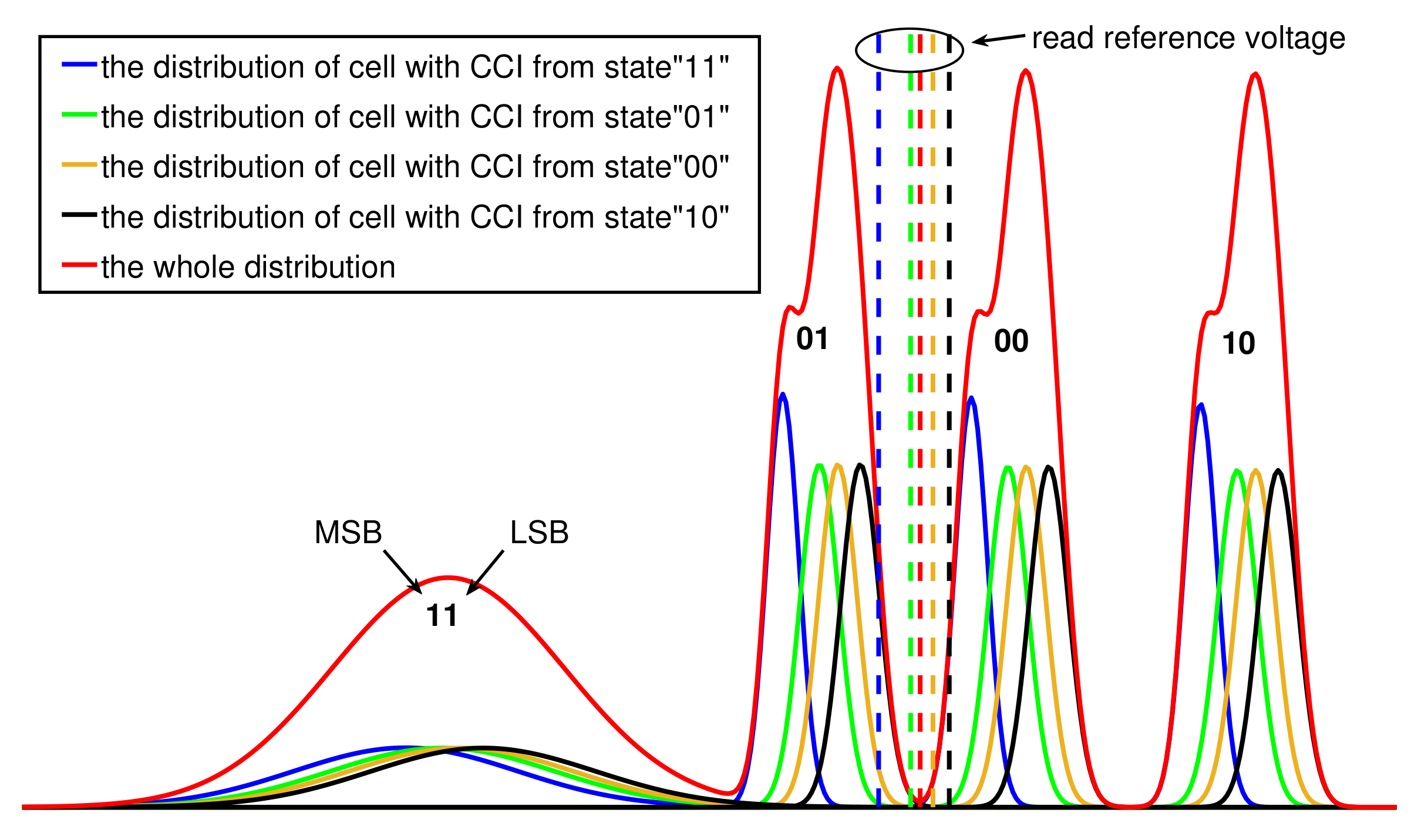
To simplify the analysis, this subsection first discusses the case that the CCI is only generated by the vertical neighboring cell. In this case, the conditional probability distribution function of the threshold voltage, (
8), is simplified to (
16):
In (
16), it is seen that the threshold voltage distribution can be divided into four parts: the distribution of cells with CCI from “11”-state, “01”-state, “00”-state and “10”-state, which are also shown in
Figure 4. In an overlap region, the bits with different CCI noise levels may have different error rates. For instance, in the overlap region between “01”-state and “00”-state, the bits of the cells in “00”-state with CCI from neighboring cells in “11”-state may be wrongly detected as “1” in LSB. In general, we want to find the optimal reading reference voltage at the intersecting point of the distributions of two states, such as the red dotted line in
Figure 5. However, once we know the programmed state or the threshold voltage of the cells that donate the CCI to victim cells, the optimal reading reference voltage may change. For example, the optimal reading reference voltage should be selected by the blue dotted line in
Figure 5, when the vertical neighboring cell is in the erased state.
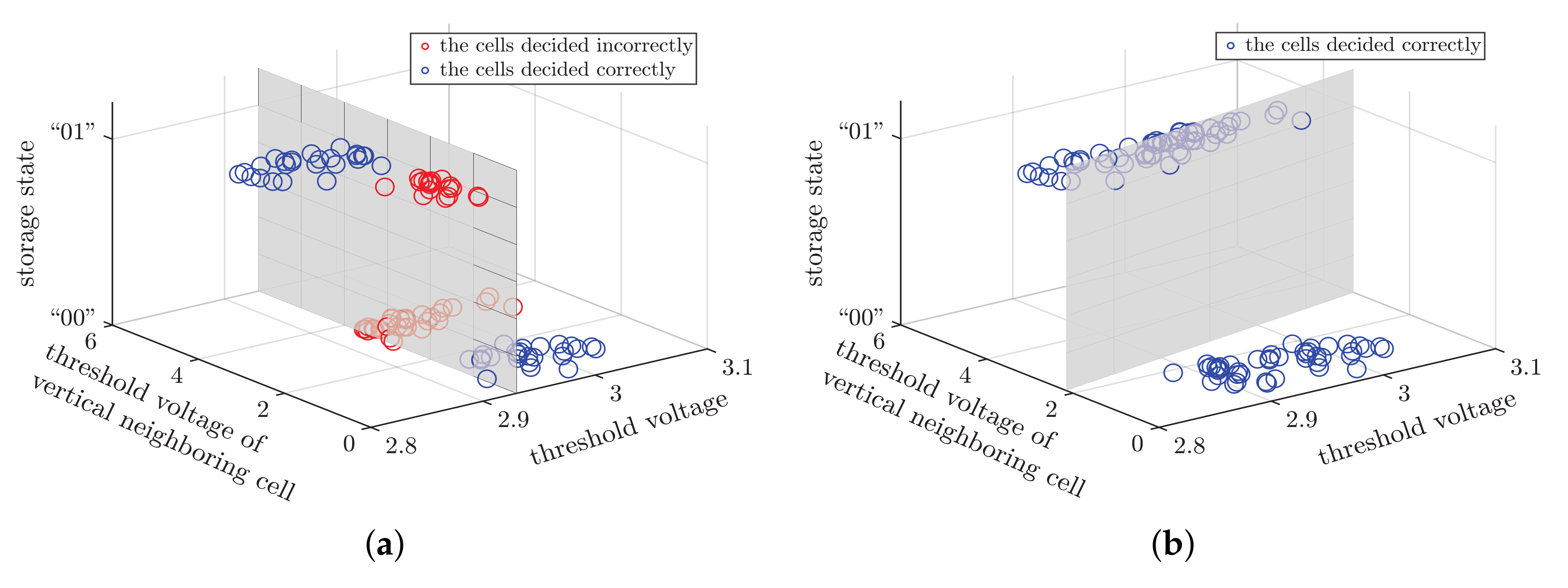
In this paper, we expand the two-dimensional coordinates to three-dimensional, as shown in
Figure 6a. The X-axis is the victim cell’s voltage, and the Y-axis is the threshold voltage of vertical neighboring cell. By doing so, one can easily find the incorrectly detected cells, marked with red dots. Moreover, we have two important observations:
- (1)
The correct cells (the blue dots) and the incorrect cells (the red dots) are not interlaced in the three-dimensional space. It means that the correct cells (or the incorrect cells) have similar features, which may be used for clustering them from the incorrect ones.
- (2)
The hard decision may not be the optimal decision when the surrounding cells have been read. In
Figure 6a, the gray plane is the hard-decision plane, but not optimal. Suppose that there is a decision plane, shown as
Figure 6b, and then we apply this plane to the same data in
Figure 6a. One can see that the decision performance by the plane gets significantly improved compared to the plane in
Figure 6a.
These two observations reveal that the detection of bits in a cell can be transformed into a clustering problem, which is to obtain an optimal classification hyperplane. When more surrounding cells are considered, the clustering problem will become more complex and the dimensions of the classification hyperplane will increase beyond three. To address this issue, We propose to use the neural network, which is good at solving various clustering problems.
3.3. Proposed Artificial Neural Network-Assisted Error Correction (ANNAEC) Scheme
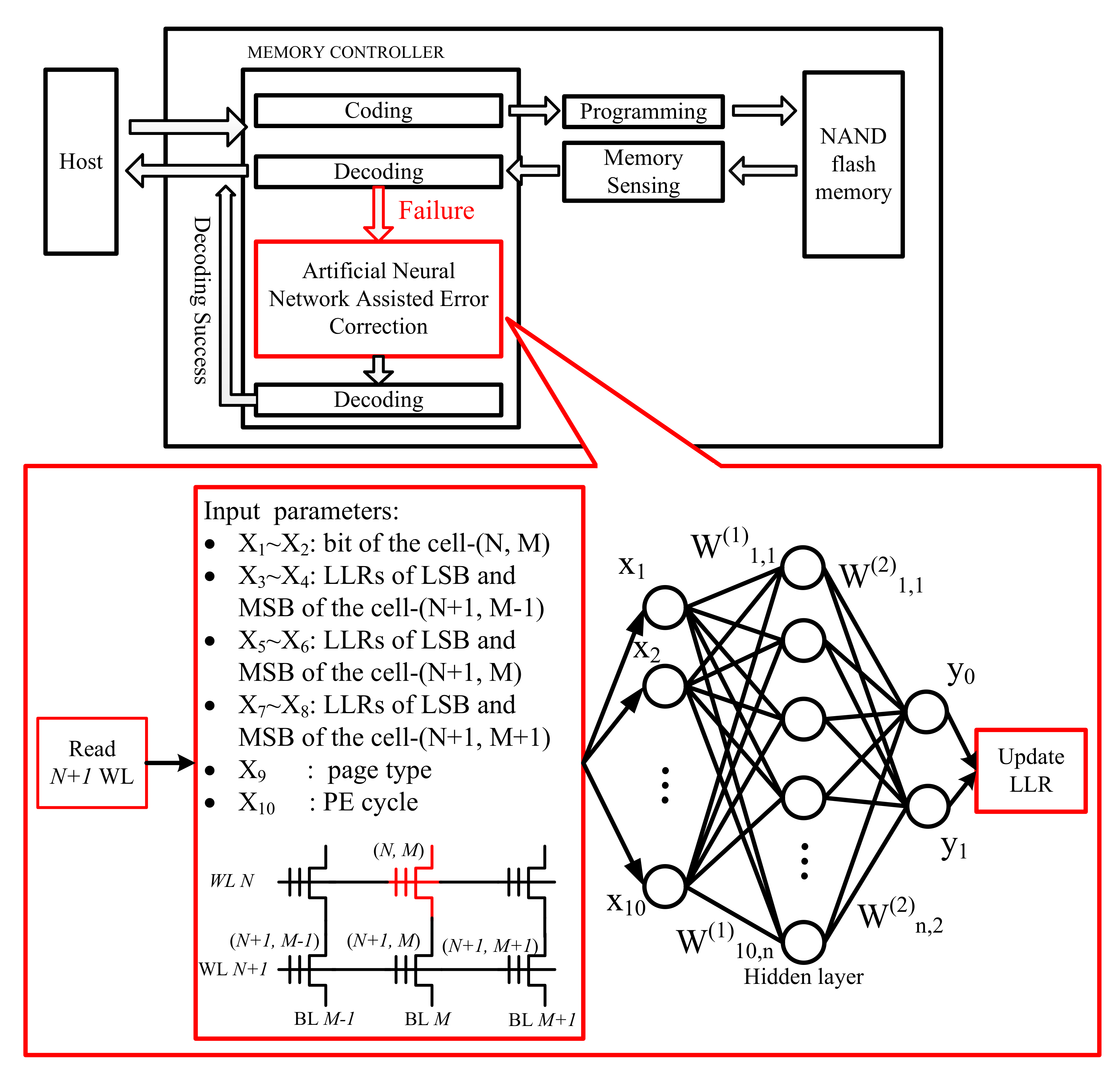
The main idea of the proposed ANNAEC scheme is shown in
Figure 7. In general, the flash memory controller uses soft-decision error correction [
12], read-retry [
1,
16] and voltage optimization, which has been widely used in practical systems, to ensure the reliability of data stored in NAND flash memory. When these techniques are not effective in suppressing flash channel noise, the flash memory controller attempts to operate the proposed ANNAEC scheme to correct error bits. Moreover, it can reduce the power consumption and computation burden of the controller, since the cells in an overlap region take a relatively small part of the cells on a page.
In general, the host implements data writing and reading to the NAND flash memory chip by communicating with the memory controller, which communicates with the NAND flash memory chip. First, the host transfers data to the flash controller. The flash controller then encodes the data and writes it into the NAND flash memory chip. When the host reads the data, the flash controller communicates with the NAND flash chip. During this process, the NAND flash chip reads the data from the cell and sends it to the flash controller by reading the sensing circuit. After that, the flash controller corrects and restores the original data through the decoding algorithm and sends it to the host. The proposed a neural network assisted error correction algorithm is used as an alternative decoding algorithm. When the decoding of the flash controller fails, the neural network model is used to first correct the data and then perform decoding.
We label the positions of the cells in an overlap region, which is at the
N-th word-line and the
M-th bit-line in the block as
, shown in
Figure 7. The input parameters of the neural network are summarized in
Table 1.
and
are the bits of cell-
in MLC memory, respectively.
∼
are the LLRs of LSB and MSB of the immediate adjacent cells, i.e., cell-
, cell-
and cell-
.
is the flag of page type. If the current reading page is LSB, we set
to “0”; otherwise,
is set to “1”.
is the number of PE cycles. There are two reasons for choosing those parameters: (1) the threshold voltage is difficult to be obtained in a practical system, but the LLR and bits in a cell can help to locate the range of threshold voltage; (2) the vertical and the diagonal neighboring cells contribute about
of the CCI [
17,
18].
Afterward, we send the parameters into the back propagation neural network to correct error bits. The sigmoid function is selected as the activation function of the back propagation neural network, given as
The cost function is chosen as the typical mean square error (MSE) cost function [
19], given by
where the outputs of neural networks
and
are the reliabilities of “0” and “1”, and
T denotes the desired reliability in the data set. The relative LLR is calculated offline in the flash memory controller. It is difficult to recalculate the relative LLR, since the online characteristic estimation of the memory channel causes longer read latency. Since the accurate relative LLR is hard to recalculate, we update relative LLR by
where
denotes original relative LLR obtained in the sensing operation, and
is given by
Although (
19) does not update the accurate LLR to decode, it can estimate the value of LLR. Moreover, (
19) is used to correct the sign of LLR, which is more important than the absolute value of LLR, since fewer error signs of LLRs fewer less error bits.
5. Conclusions
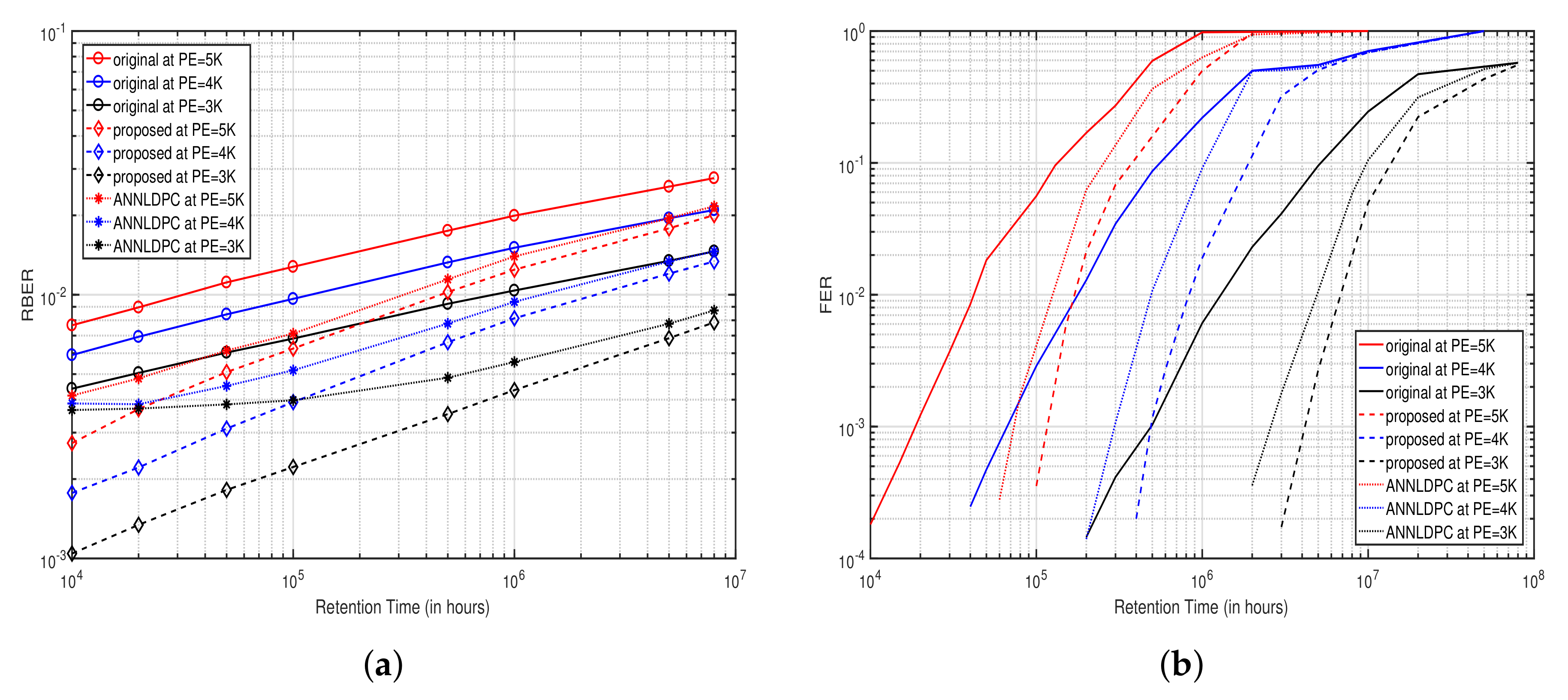
In this paper, we have proposed to use the relative LLR calculation to estimate the actual LLR. Furthermore, in three-dimensional coordinates, we have transformed the bit detection problem into a clustering problem, which allows us to apply an artificial neural network in the memory channel. To solve the clustering problem, we proposed an artificial neural network-assisted error correction scheme, which has been shown by experiments to be effective in correcting the error bit when the conventional method without the neural network fails to decode. Simulation results have shown that the FER performance of our ANNAEC is significantly better than that of ANN-LDPC. For example, the ANN-LDPC can make the flash memory endure up to h, and the proposed method provides the performance gain of approximately of data retention, which makes the retention time of flash endure up to h. Furthermore, our proposed approach can be extended to TLC or QLC flash memories.


