1. Introduction
Integrated circuit designs are becoming more complex day by day, and the integration of ten billion transistors on the same die with clock frequencies above several gigahertz makes it difficult to implement cost-effective and reliable systems. The development of reliable and cost-effective mixed-signal and RF systems depends on system-on-chip (SOC) and system-in-package (SIP) technologies [
1,
2,
3,
4,
5]. We need accurate and reliable design tools for the estimation of switching noise coupled from the digital part into analog to implement noise-free integrated circuits for use in future-generation electromechanical systems. Switching noise is of significant importance, as it propagates to the RF section via I/O pins and substrate and can cumulatively reach several hundred millivolts [
6,
7,
8,
9,
10,
11]. Transistor model quality and choice of input signal play a significant role in the exact estimation of switching harmonics. BSIM (Berkeley short-channel insulated-gate field-effect transistor (IGFET) model) transistors models are reliable, accurate and currently considered the industry standard. All simulations presented in this paper are performed on BSIM 3 and BSIM 4 transistor models using Cadence Spectre (V 6.1, Cadence Design Systems, Inc., San Jose, CA, USA) and MATLAB simulators (V 2010a, MathWorks, Inc., Natick, MA, USA).
2. Transistor Model Quality
Transistor model parameters influence the spectrum of switching waveforms emitted by digital circuits. With the help of advanced numerical tools, we are able to deduce explicit output-switching waveforms for simple transistor models [
10]. Circuit simulations of simple transistor models yield transition edges that are helpful to construct a pulse waveform. The spectrum of the pulse is evaluated through FFT.
Simulations performed with Level 1, Level 2 and Level 3 transistor models show that several discontinuities exist in the form of derivatives of the drain current as a function of terminal voltages. These models did not mitigate the short-channel effects. The spectrum roll-off achieved with these transistor models did not exceed more than 70 dB/decade. However, results with the Maher-mead model display improvement in the spectrum roll-off around 100 dB/decade. Our simulations were performed on de facto industry-standard next-generation device models of the BSIM family. BSIM stands for Berkeley short-channel insulated-gate field-effect transistor model. BSIM models are reliable and provide highly accurate simulation results. Many companies and universities rely on their own MOS transistor models for circuit simulations.
Device threshold voltage is an essential parameter in circuit simulations. Low-threshold devices yield large subthreshold currents. Low-threshold devices turn on softly and produce a steep spectrum roll-off [
1]. Due to characteristics, low-threshold voltage devices are good for use in complex integrated circuits. The drawbacks of low-threshold devices include the production of leakage currents and idle power dissipation. The switching noise in integrated circuits is circuit controlled by the accurate estimation of the harmonic contents of CMOS logic-switching waveforms. IC designers distribute the noise budget among different blocks of design, and this technique is helpful in the reduction of switching noise.
BSIM Models
Many semiconductor manufacturing companies and academic institutes have developed their own transistor models and claim they are the best in the world. This situation makes it difficult to decide what the best transistor model is. Fortunately, UC Berkeley developed BSIM in 1990. BSIM transistor models accurately fit into the I–V characteristic curves of modern transistors. The BSIM 3 transistor model contains more than 200 parameters that affect the simulation results and are an essential part of the device physics of modern transistors. These parameters model the second-order effects of modern transistors. BSIM transistor models are reliable and accurate; however, they do not appropriately model the leakage currents of modern transistors. BSIM 4 is an extension of the BSIM 3 model, and BSIM 5 and BSIM 6 are further extensions. BSIM transistor models provide detailed information about all second-order effects such as drain-induced barrier lowering (DIBL), mobility degradation, short-channel effects, velocity saturation, etc. Modern BSIM transistor models have multiple gate capacitance models such as resistance models and diffusion capacitance. The temperature dependence of diode junction capacitance is also included in modern BSIM transistor models. Modern BSIM transistor models include parameter checking in the package to avoid bad parameter values.
3. Switching Noise
Switching noise is a complex issue in the design of digital integrated circuits. Switching noise consists of three different parts: the first part is the circuit that generates noise, called the aggressor circuit. The second part is the circuit that couples the noise from the aggressor, called the victim circuit. The third part is the circuit that picks the noise from the victim circuit. The total noise, received at the victim circuit, is a combination of noise from many aggressor circuits. Circuit reduction techniques are important in noise generation. Reduced digital circuits generate less noise, and large digital circuits generate more noise, for which we require large computer and software resources to simulate.
To control noise generation in digital integrated circuits, the study of harmonic contents of the switching waveform spectrum is essential. The time-domain waveform of a signal determines its spectrum. According to the rule stated by Lee [
11]: “the spectrum of a signal will decay as
, where n is the number of derivatives of the signal required to yield an impulse.” The existence of discontinuities in the model distorts the spectra, and hence, the discontinuities occur only in the simulation domain. To study the higher-order harmonics in the spectrum of digital circuits, we need to avoid discontinuities in the models; otherwise, the results will not be trustworthy.
Regardless of the shape of the input waveform, there will be higher-order harmonics in all output-switching waveforms generated by the digital circuits, as output waveforms approximately resemble square waves. Due to comparatively slow edges, sinusoid-shaped waves produce extra short-circuit power. Higher-order harmonics are also generated when the sinusoid-shaped waves are amplified and limited. Due to sharp edges, square-shaped waves create discontinuity in the output-switching waveform or its derivatives, which decreases the spectrum roll-off of the output-switching waveforms. The best candidate for input to digital circuits is a square-like wave (neither sinusoid-shaped nor perfect-square-shaped). Hence, we generated a square-like wave by using the mathematical function of arctan(sin). The arctan(sin) function produces a continuous waveform, as both the tangent and sine functions are continuous.
4. Tool Setup and Input Signal Selection
By using the Verilog-A tool, we generated a square-like wave with the mathematical arctan(sin) function.
Figure 1 shows Verilog-AMS HDL code for the generation of the input signal.
4.1. Simulations Using 65 nm Process Technology
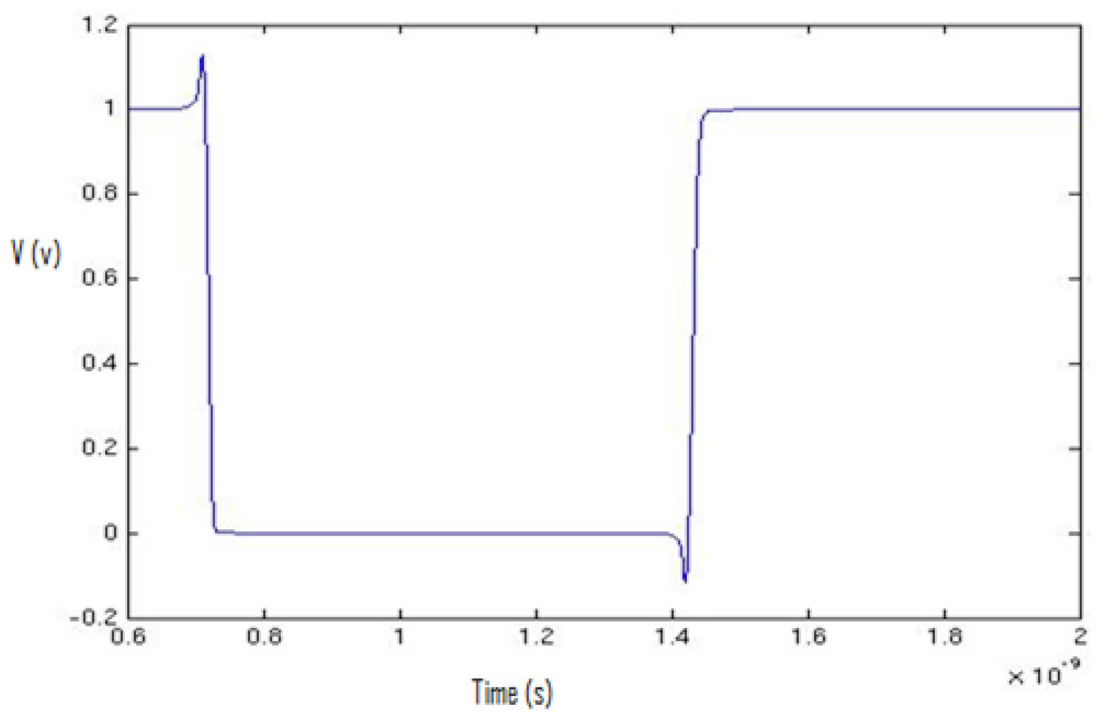
For the tool set-up, we started the simulations of a simple inverter, and then we extended the idea of the simulations to complex flip-flop and latch structures. First, we plotted the waveforms using the Cadence Spectre Simulator and then transferred the equidistant data points to MATLAB, as shown in
Figure 2. We used high accuracy settings in the Cadence Spectre to obtain 5000 equidistant data points in a specific cycle to obtain a clear view of data points in the switching spectrum. After that, we plotted the spectrum of the specific cycle that contained 5000 equidistant data points using MATLAB.
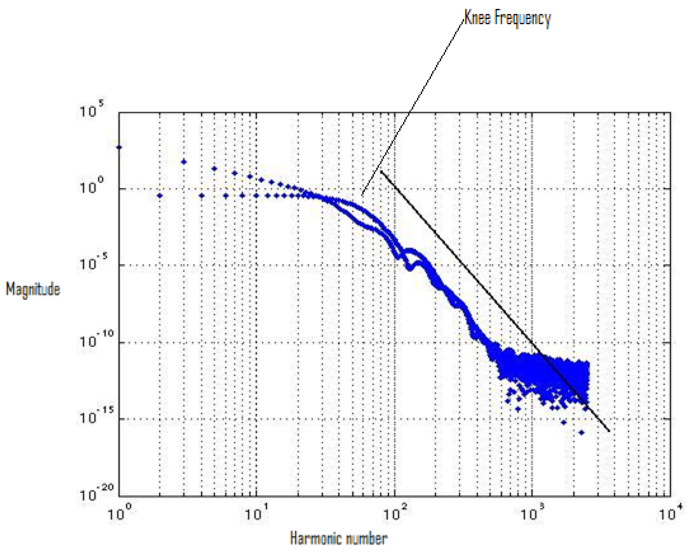
By using FFT, we evaluated the spectrum of the output-switching waveform.
Figure 3 describes the switching waveform of an inverter using a 65 nm process technology design kit. The 65 nm process design technology kit uses the BSIM 4 transistor model.
Figure 3 shows the spectrum roll-off of 20 dB/decade before the knee frequency, and beyond the knee frequency, the spectrum roll-off is 100 dB/decade, which is much steeper. At knee frequency, the spectral amplitude is down by half (−6.8 dB) below the natural 20 dB/decade roll-off [
11]. A 100 dB/decade spectrum roll-off means that there is no discontinuity in the first four derivatives of the provided input signal. We used the input signal of the square-like wave generated by the arctan(sin) wave to ensure that there was no discontinuity in the input signal. Discontinuity decreases the spectrum roll-off and generates higher-order harmonics. To avoid higher-order harmonics, a steeper roll-off of the switching spectrum is desirable, and to control noise in digital circuits, the correct estimation of harmonics is required [
12,
13,
14,
15,
16,
17].
4.2. Simulations Using 130 nm Process Technology
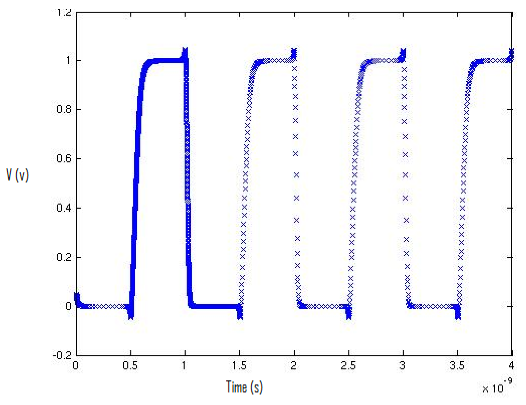
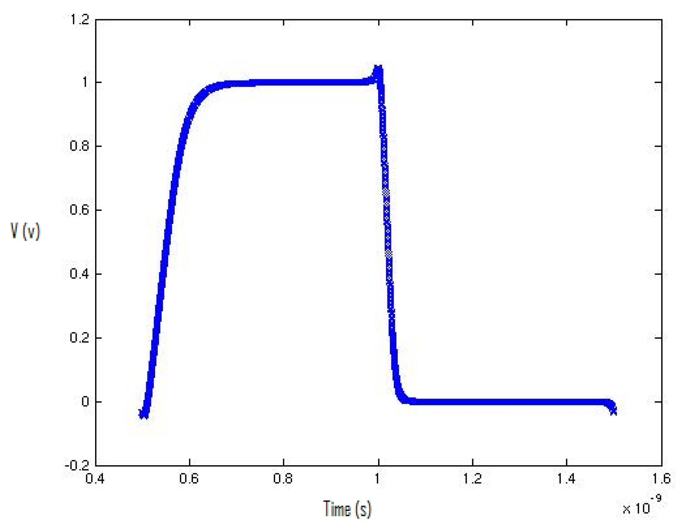
Figure 4 describes the inverter’s output-switching waveform using the 130 nm process. The first cycle of the waveform contains 5000 equidistant data points.
4.3. Comparison
Table 1 compares the simulation results of 65 and 130 nm process technologies in terms of the rise time and roll-off of the switching spectrum waveforms.
5. Flip-Flop and Latch Topologies
For our analysis, we selected a set of latches and flip-flops that were designed to construct high-performance and low-power microprocessors [
14,
15,
18]. To meet our design goals, we applied:
A pulsed design;
Smallest as possible direct path;
Smallest as possible node swing;
Smallest as possible clock load;
Low-power feedback and optimized master–slave stages.
To meet our design objectives, we did not want the setup time of the design to be positive, clock slope and clock skew sensitive, dynamic and floating nodes and master latch as dynamics.
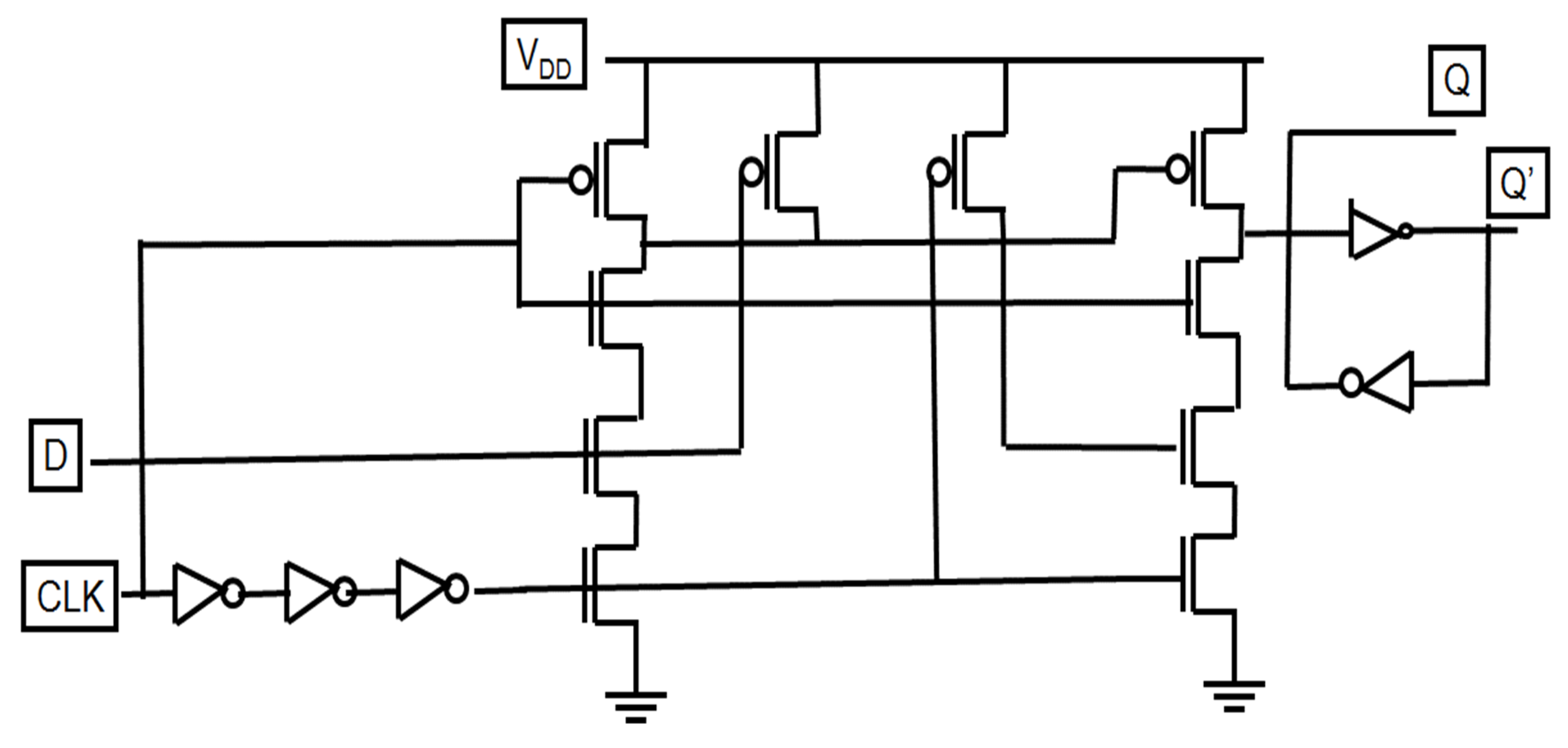
The PowerPC 603 master–slave latch is a fast classical structure, as shown in
Figure 7. The PowerPC 603 master–slave latch has a short direct path and low-power feedback, which makes it ideal for use in high-performance microprocessors. However, the clock load of the PowerPC 603 master–slave structure is large, which increases the total power in-chip dissipation.
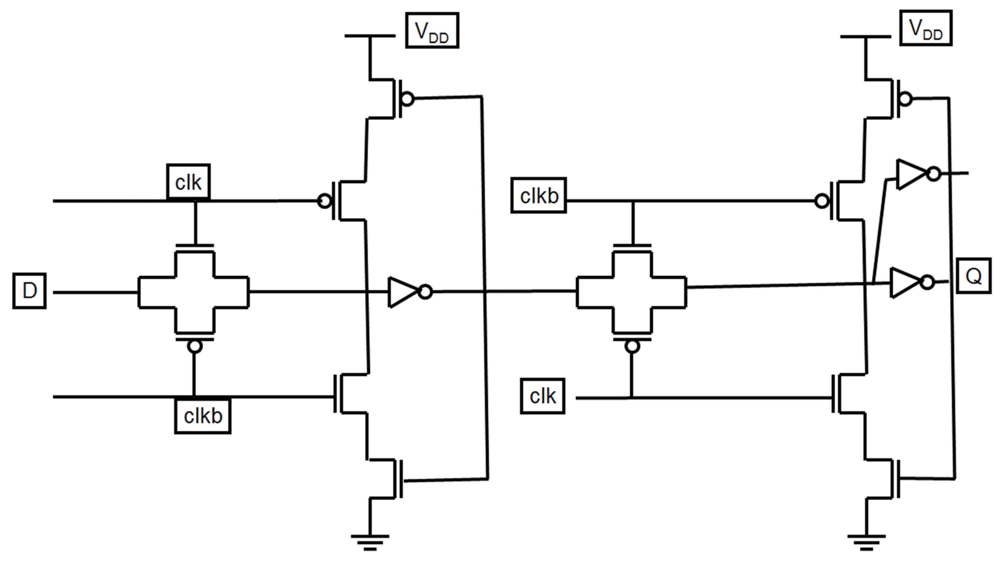
Figure 8 presents a modified C
2MOS latch structure. The modification in the dynamic C
2MOS master–slave latch [
14,
15,
18,
19,
20] results in better low-power characteristics and a small clock load, obtained by the low-power feedback and local clock buffering, assuring fully static operation. The PowerPC 603 master–slave latch is faster than the modified C
2MOS master–slave latch. The PowerPC master–slave latch uses complementary pass-gate transistors, which results in a faster pull-up and increase in the sensitivity to race through one gate delay period in which both phases overlap.
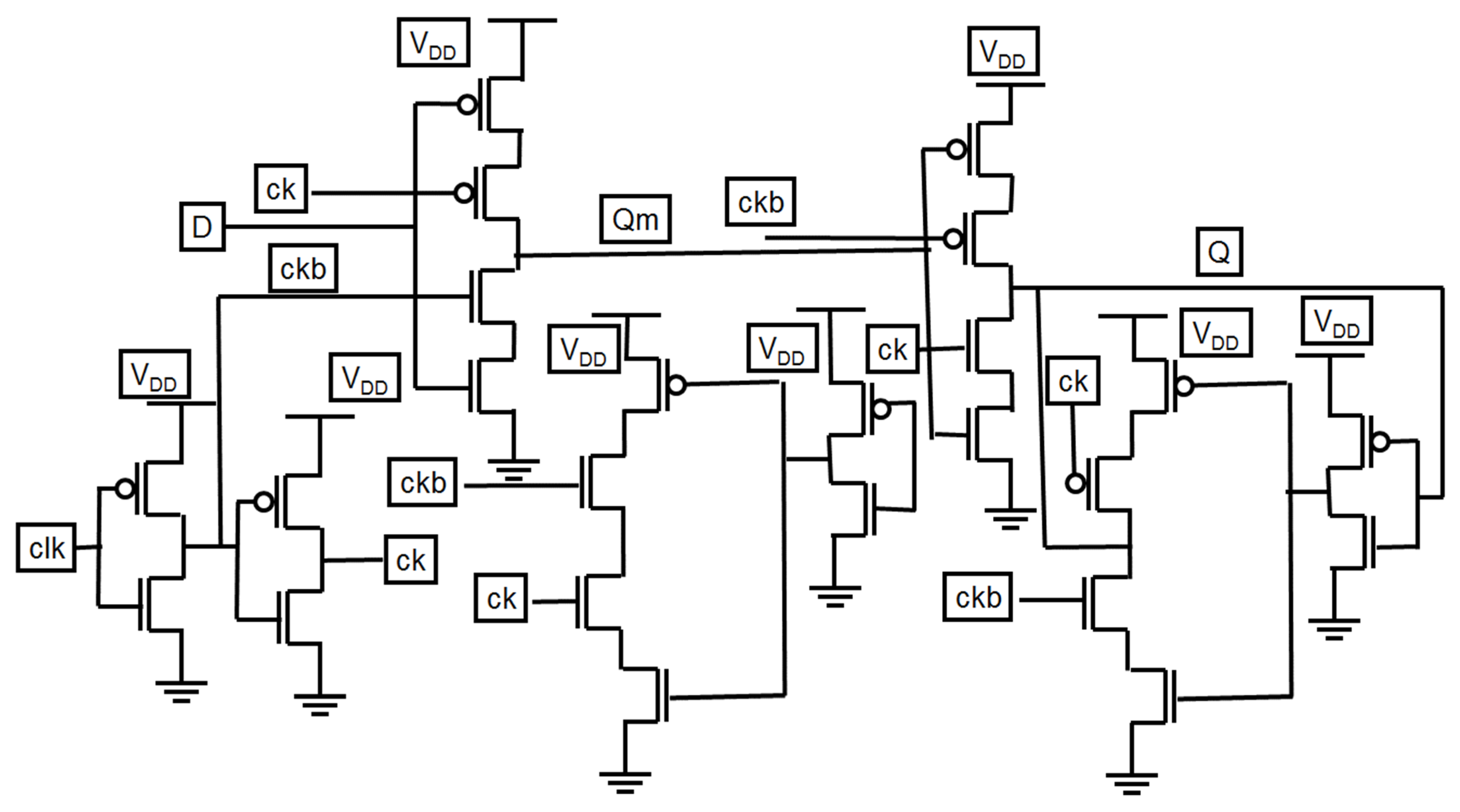
Figure 9 presents a hybrid-latch flip-flop (HLFF) structure. Hybrid-latch flip-flop (HLFF) is one of the fastest structures discussed in this paper. The power delay product (PDP) of HLFF is very small. One of the main advantages of HLFF is its robustness to clock skew, and one of the disadvantages of HLFF is its positive hold time. Due to the single output design, the power dissipation of HLFF is almost similar to static logic circuits [
14,
15,
21,
22,
23,
24].
Other flip-flop and latch structures presented in this article include semi-dynamic flip-flop (SDFF), K6 edge-triggered latch (K6-ETL), StrongArm110, precharged sense-amplifier stage SA-F/F, static single-transistor-clocked flip-flop (SSTC) and dynamic single-transistor-clocked flip-flop (DSTC) [
25,
26]. SDFF is the fastest among all the structures presented in this article. The K6 edge-triggered latch is a differential, dynamic, self-resetting and hybrid structure. The K6 edge-triggered-latch is a fast structure, but it has a drawback, i.e., very high power consumption independent of the data pattern. Monotonous transition at the outputs of K6-ETL, SA-F/F and StrongArm110 FF is an important feature, which drives the fast domino logic. Due to the capacitive coupling effect, DSTC and SSTC suffer from voltage drop at the output.
6. Simulation and Results
We performed optimization. The first step is the identification of the critical path. Using the Brent–Powell optimization algorithm embedded in the Cadence Virtuoso ADE GXL* environment, the widths of the transistors were optimized on the critical path within the specified range (0.065 to 0.90 µm for 65 nm) and (0.15 to 2.06 µm for 130 nm) for minimum total power and Clk-Q delay as shown in
Table 2.
Transistor widths that connected in the feedback paths were kept minimum.
There is a significant improvement in the spectrum roll-off with BSIM4 models using the 65 nm process.
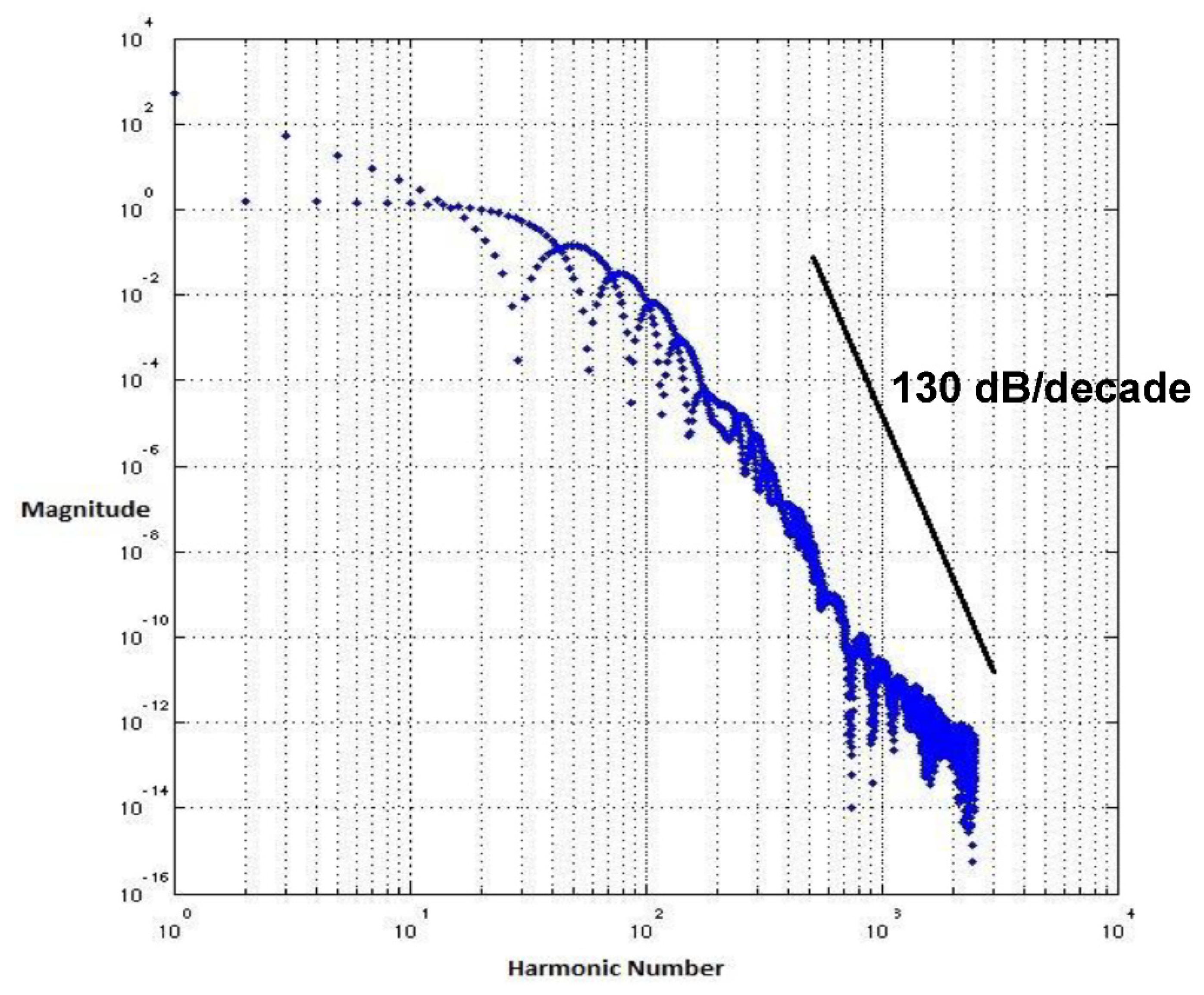
Figure 10 presents the spectrum of switching waveform of the hybrid-latch flip-flop (HLFF) using 65 nm process technology. The spectrum roll-off of HLFF is about 20 dB/decade before the knee frequency and after the knee frequency. The spectrum roll-off of HLFF is around 130 dB/decade, which is much faster than 20 dB/decade. At knee frequency, the spectral amplitude is down by half (−6.8 dB) below the natural 20 dB/decade roll-off [
27]. The spectrum roll-off of 130 dB/decade shows that there is no discontinuity in the first five derivatives of the output signal.
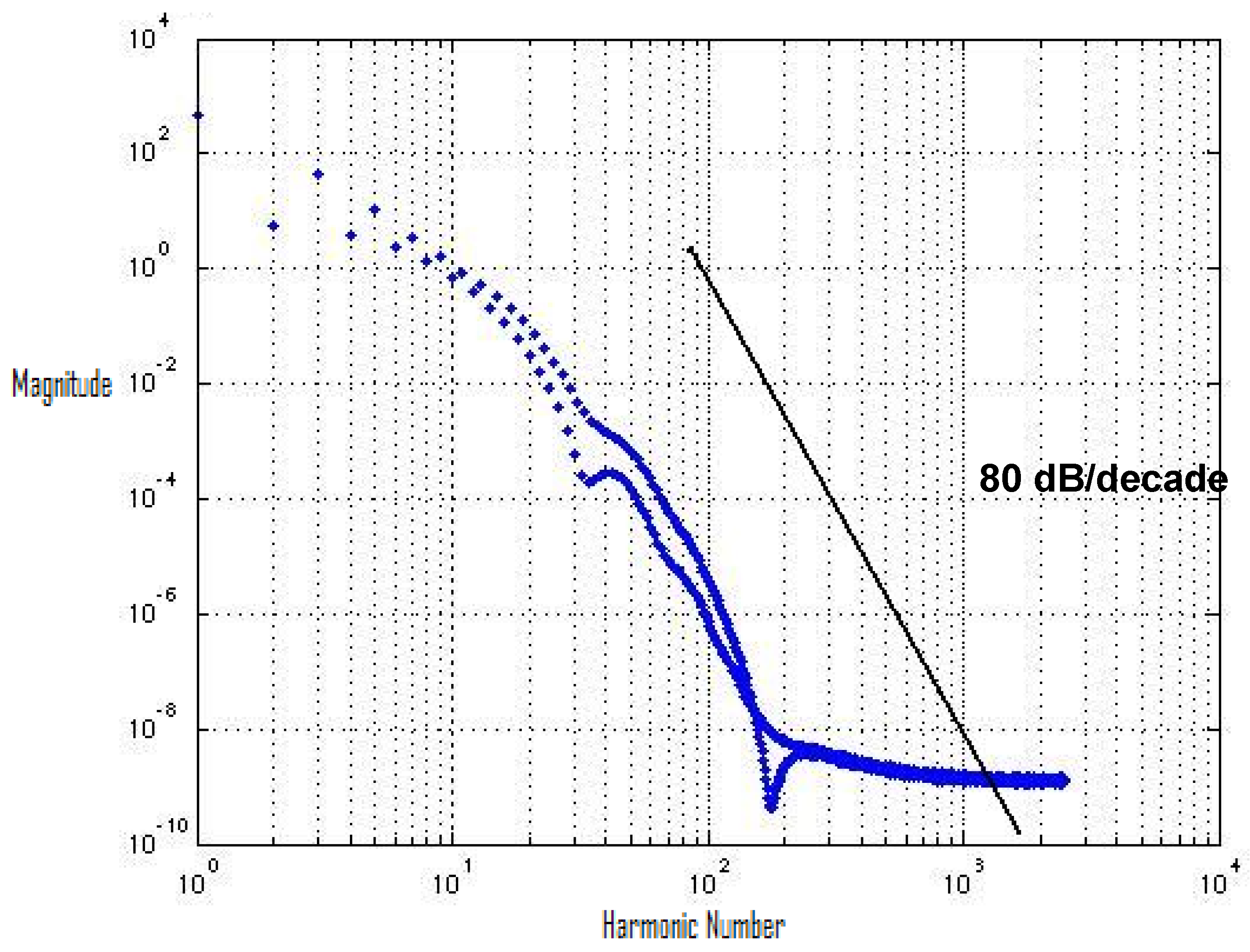
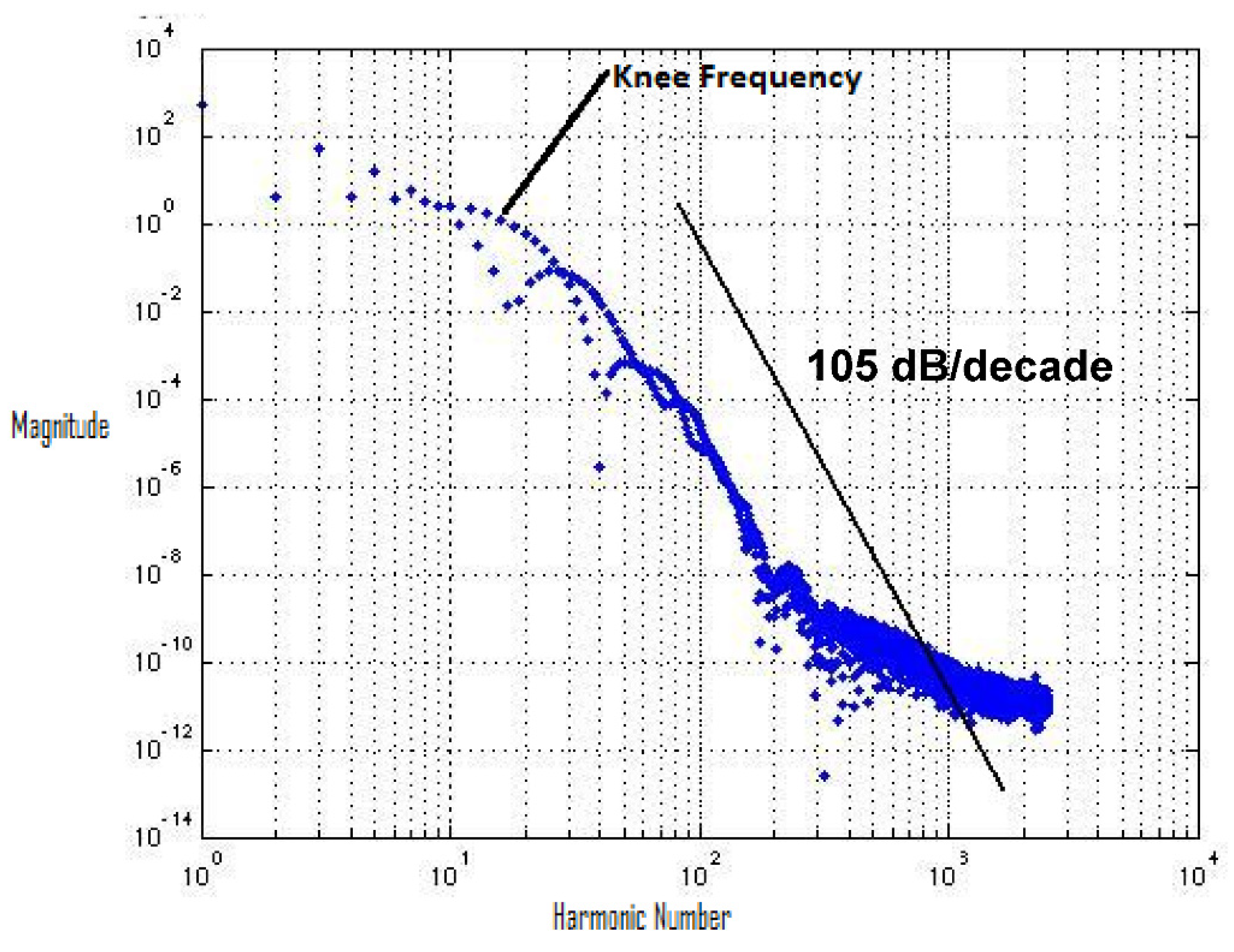
Figure 11 presents the spectrum of switching waveform of the hybrid-latch flip-flop (HLFF) using 130 nm process technology. The HLFF spectrum roll-off using 130 nm process technology is 105 dB/decade (105 dB/decade spectrum roll-off indicates that there is no discontinuity in the first four derivatives of the output signal of HLFF).
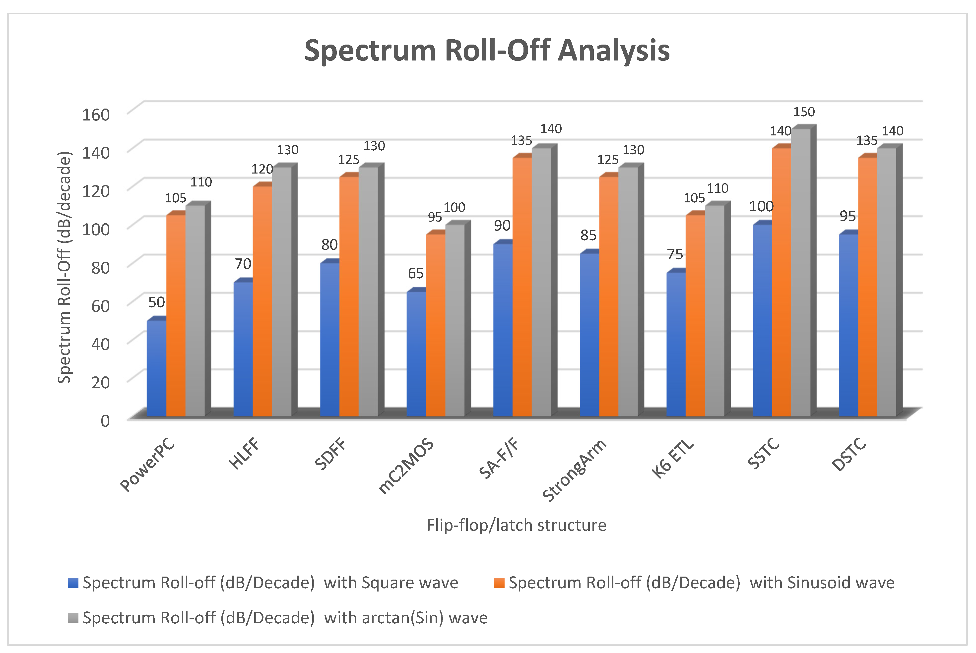
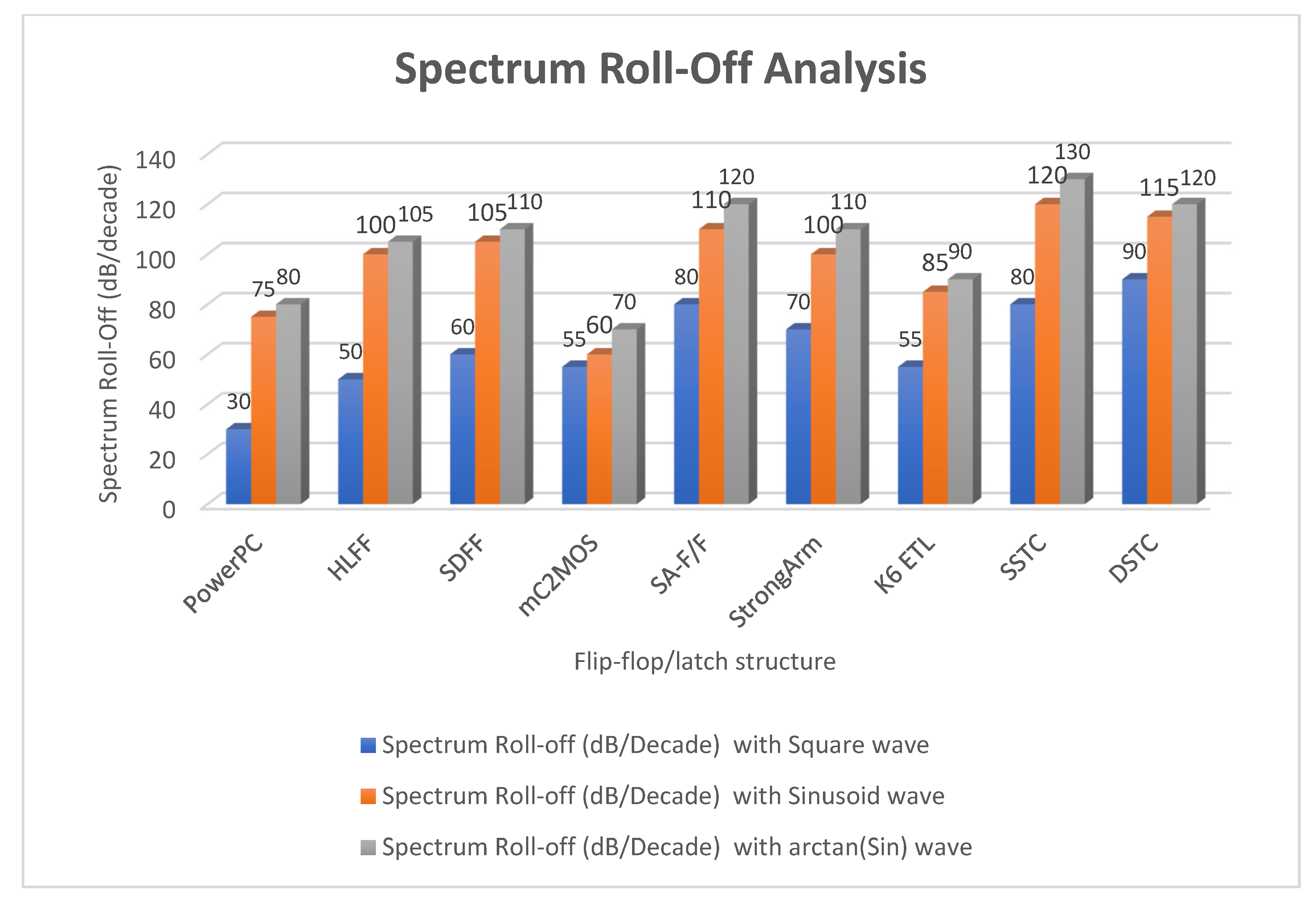
Figure 12 and
Figure 13 present the spectrum roll-off analysis using 65 and 130 nm process technologies with different types of input signals.
Figure 14 presents the spectrum roll-off analysis using 65 and 130 nm process design kits and arctan(sin) as the input signal. To avoid higher-order harmonics, we want the spectrum roll-off of the switching waveform to be as steep as possible.
7. Power Dissipation Analysis
Power dissipation is a major problem in digital integrated circuits. It decreases the performance and reliability of digital integrated circuits; hence, low-power designs are a major challenge for digital designers.
Power dissipation in a digital integrated circuit is mostly dependent on its structure and statistics of the data signal applied.
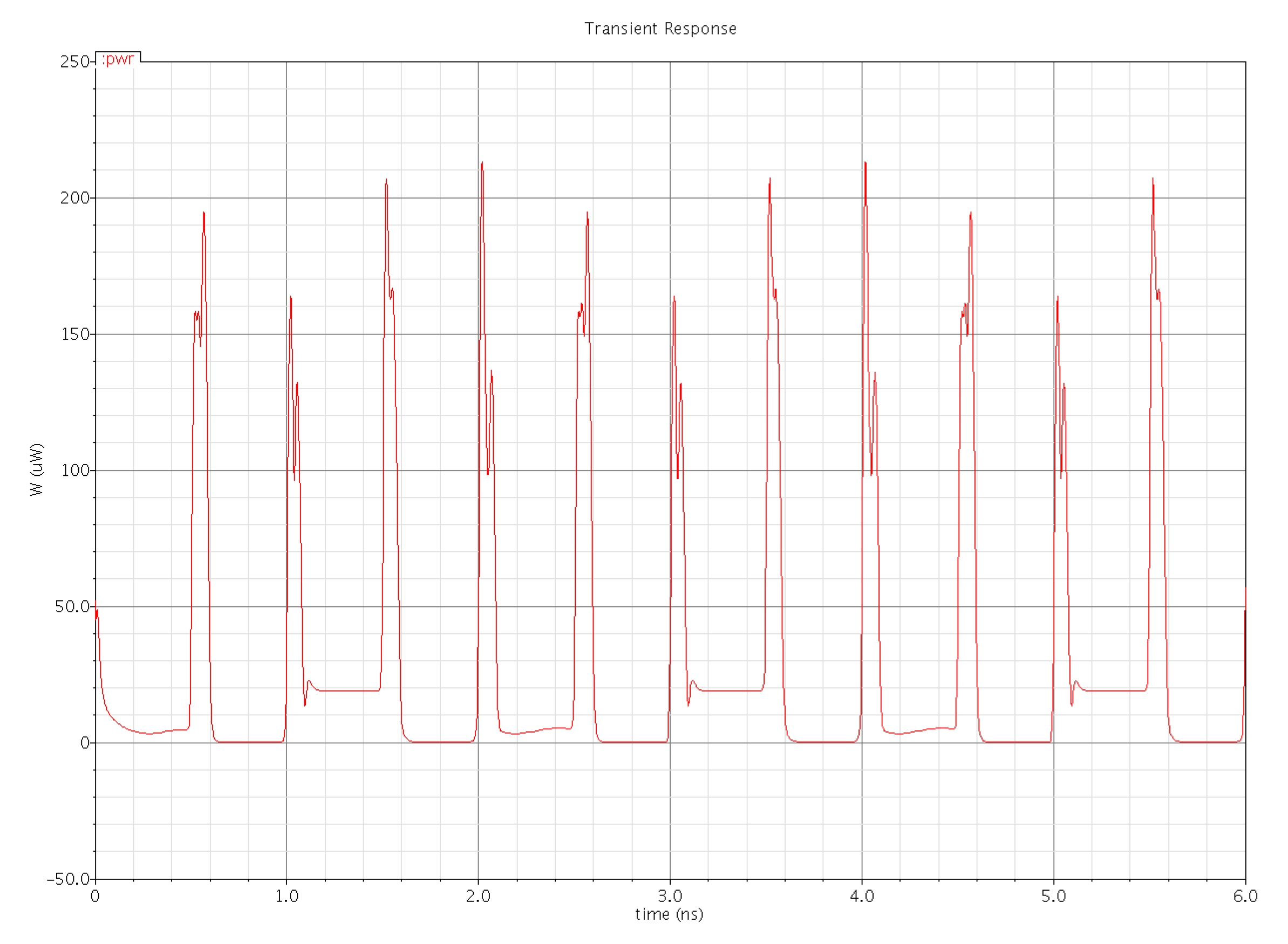
Figure 15 shows the plot of the total power dissipation of the PowerPC 603 master–slave latch. The total power dissipation is the sum of three power dissipations, i.e., internal power dissipation of the latch, local clock power dissipation and local data power dissipation. In
Figure 15, the pulse-train-like appearance of the plot is due to switching activity. When no switching happens, the signal remains unchanged, and the dynamic power is zero, but rapidly changing signals provoke plenty of switching, and therefore, power dissipation occurs. We applied a voltage of 1 V for this simulation. The average power dissipation of the plot is 25.08 µW. In some intervals, the power dissipation waveform does not go back to zero because either the static current flow or the capacitors remain partially charged during the interval.
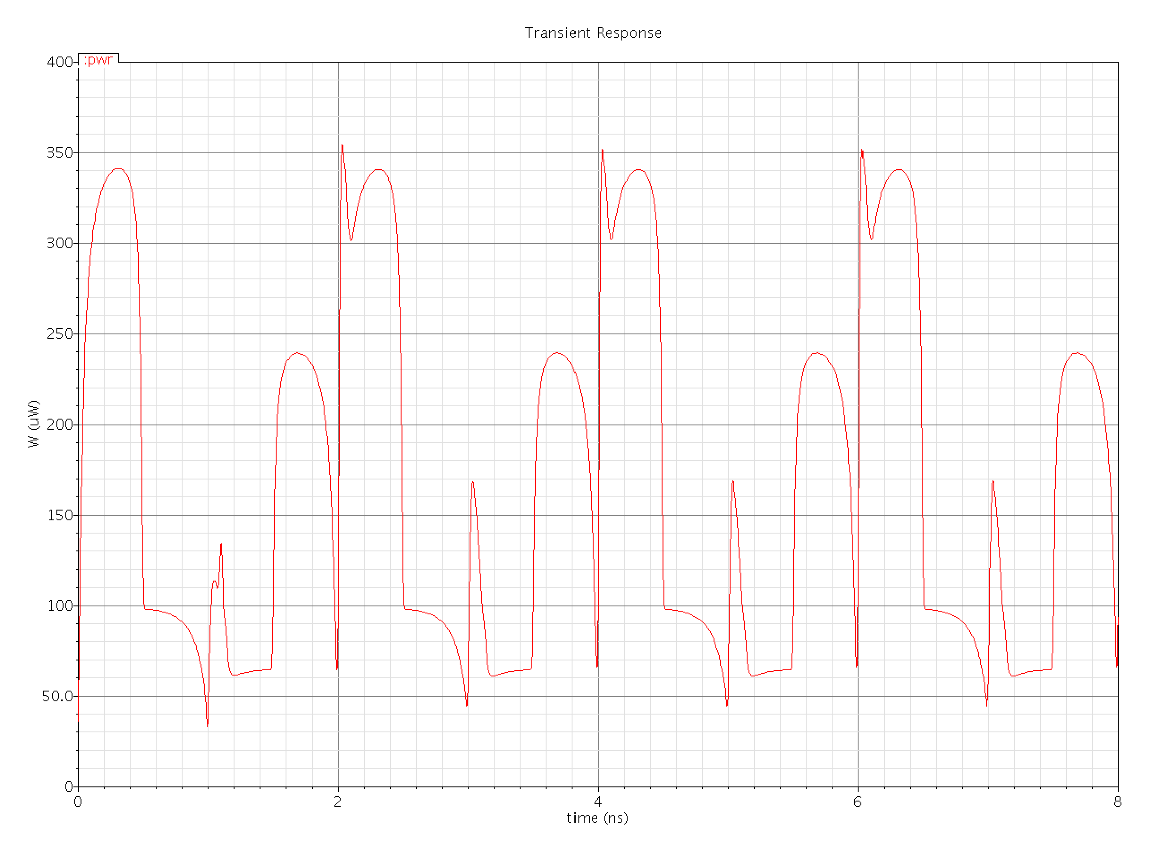
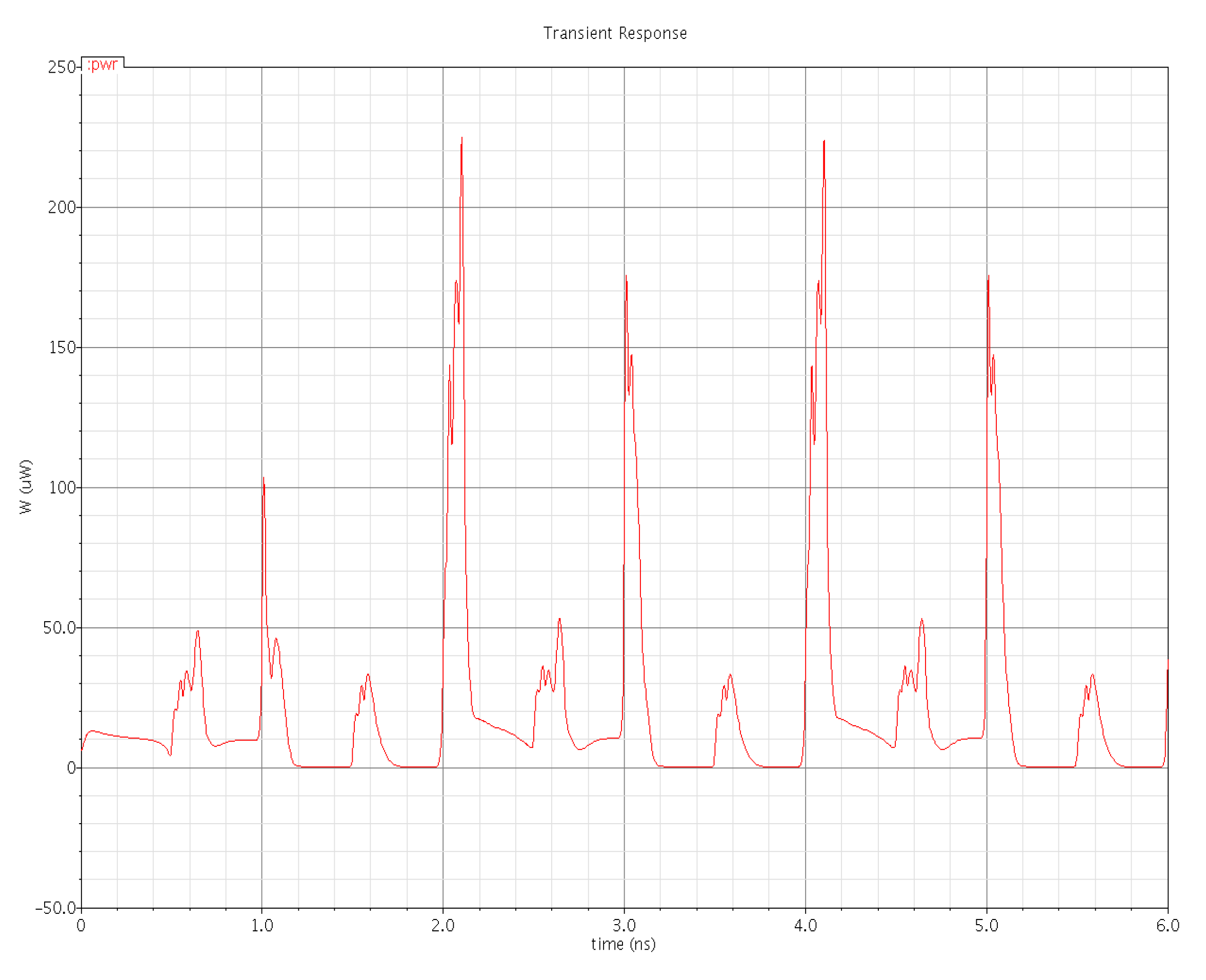
Figure 16 and
Figure 17 show the waveforms of power dissipations in the modified C²MOS latch and hybrid-latch flip-flop (HLFF).
Figure 18 and
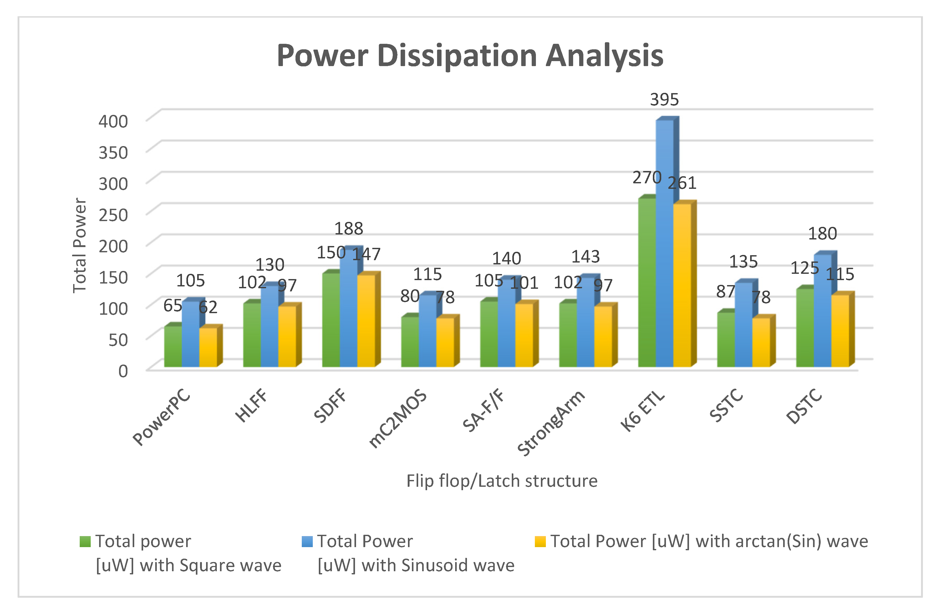
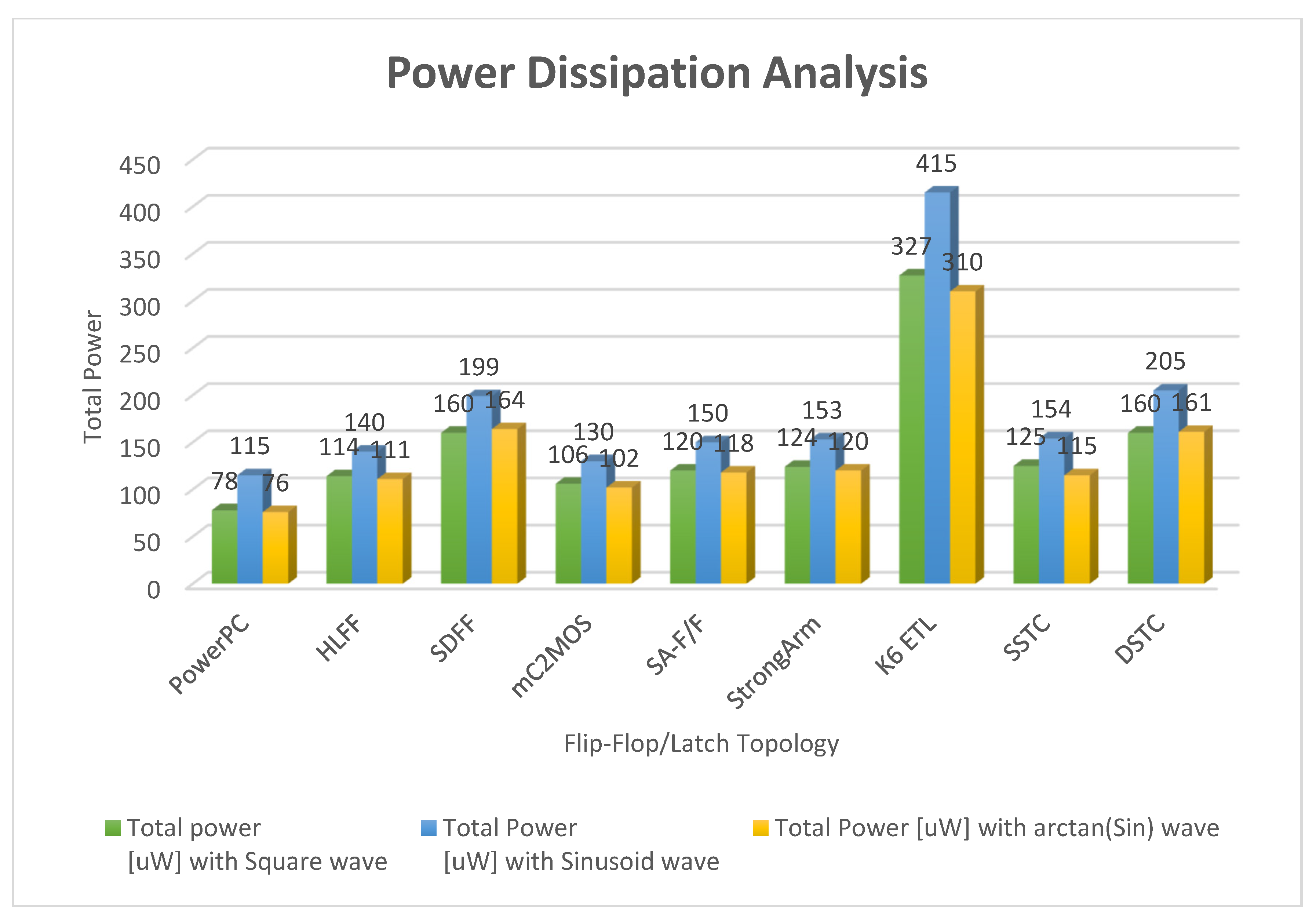
Figure 19 show the total power dissipation analysis using 65 and 130 nm process technologies and various types of input signals.
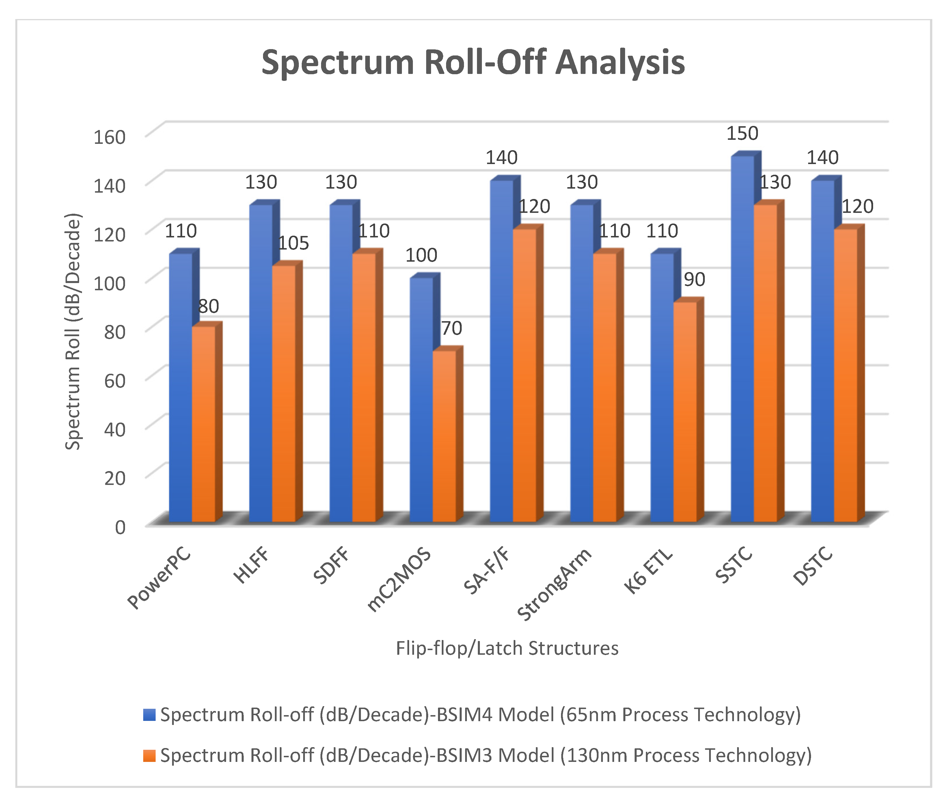
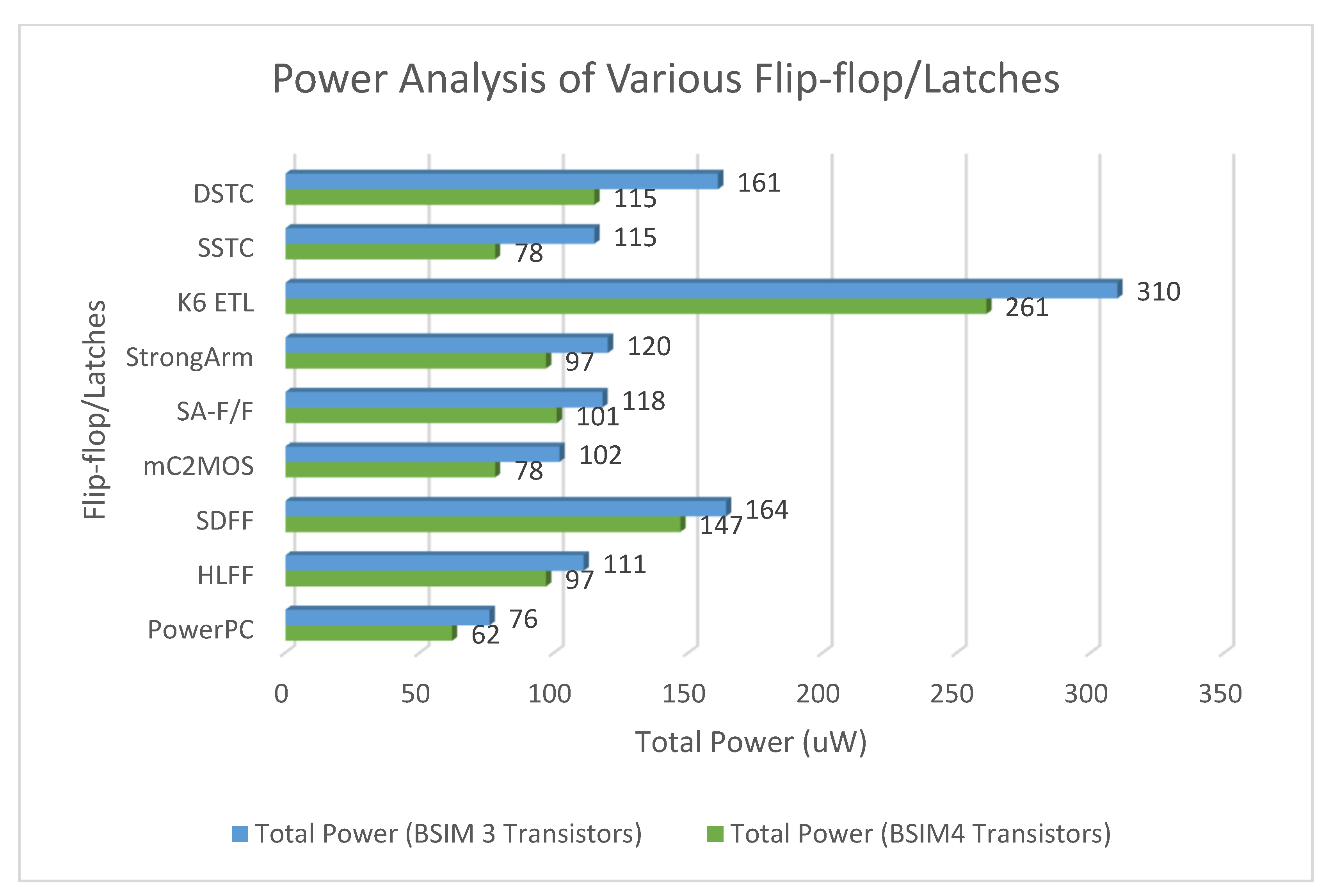
Figure 20 shows the power analysis of various flip-flop and latch topologies using 65 and 130 nm process technologies and arctan(sin) as the input signal.
Transistor model quality and input signal selection play an important role in the accurate estimation of harmonic contents of switching waveforms. We used a square-shaped signal as an input to our simulations (neither a sinusoid nor a perfect square wave). A perfect square wave causes discontinuity in the spectrum due to abrupt change, and a sinusoid-shaped wave has slower edges, which produce extra short-circuit power. The discontinuity reduces the spectrum roll-off of switching waveform, and the higher-order harmonics generate noise contents [
28,
29,
30,
31,
32,
33,
34,
35].
In this paper, we presented simulation results of the spectrum roll-off (dB/decade) of nine different flip-flops using BSIM3 and BSIM4 transistor models in two different CMOS process technologies (130 and 65 nm). To control digital noise in digital integrated circuits, the exact estimation of switching harmonics is essential. The total power dissipation in the flip-flop/latch structures is the sum of three power dissipations, i.e., internal power dissipation, local clock and local data power dissipation. The PowerPC 603 master–slave latch dissipates small power compared to the other flip-flop and latch structures, and it has a switching spectrum roll-off of 115 dB/decade for the 65 nm process design kit. SDFF is the fastest structure among all topologies presented with a delay of 140 ps, and DTSC is the slowest structure, with a delay of 510 ps in the 65 nm process. SSTC provides a steeper roll-off of 150 dB/decade in the 65 nm process. The spectrum roll-off of 150 dB/decade shows that there is no discontinuity in the first six derivatives of the output signal.
Figure 18 and
Figure 19 present the total power dissipation analysis using 65 and 130 nm process technologies, respectively, using various types of input signals.
Figure 20 presents the power analysis using various flip-flop/latch topologies.
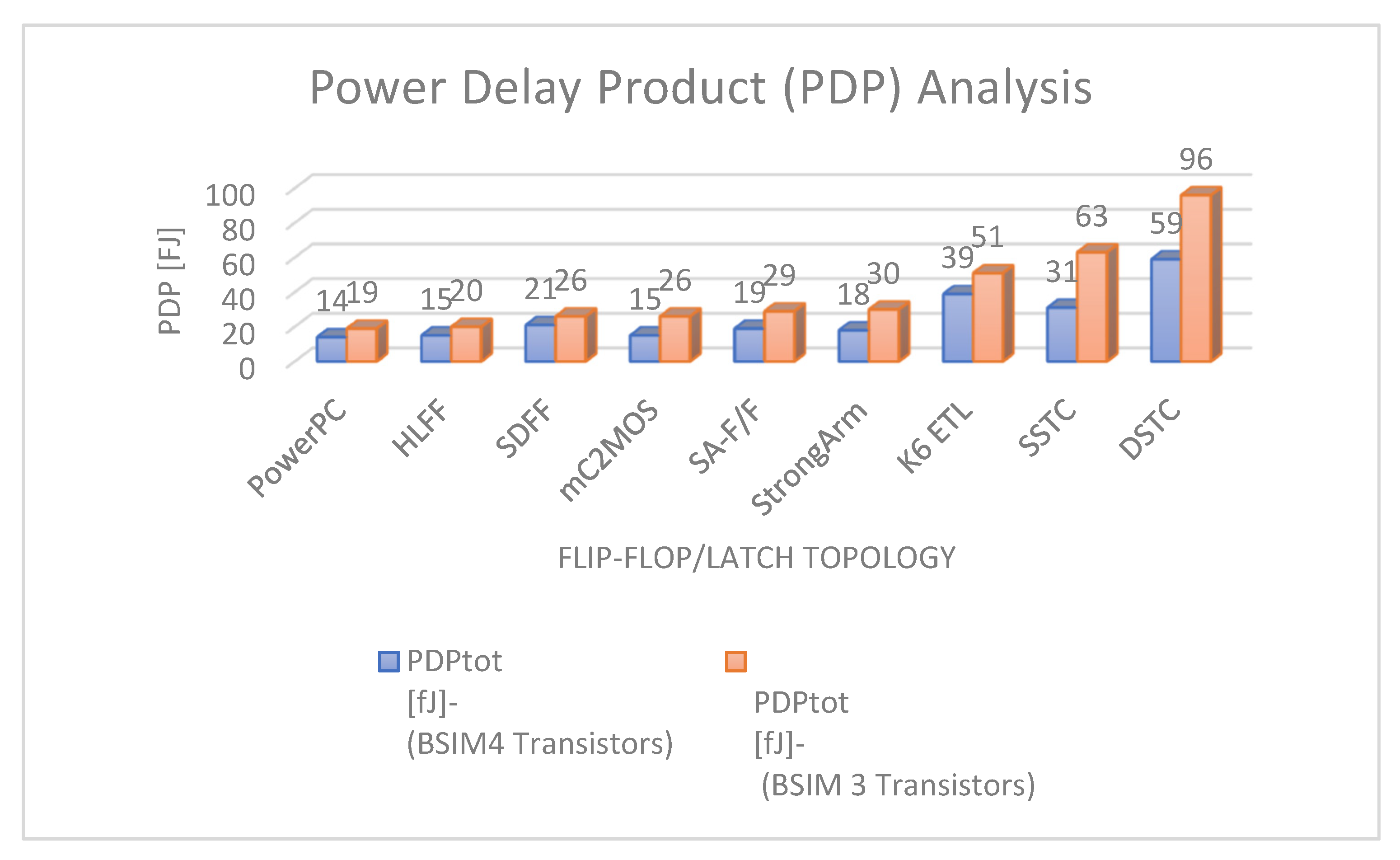
Figure 21 presents the power delay product (PDP) of all nine flip-flop and latch topologies discussed in this paper.
8. Conclusions
The analysis presented in this research article can help the designer to design a highly integrated noise-controlled digital CMOS circuit for use in future-generation micro- and nanoelectromechanical systems. An accurate estimate of higher-order harmonic contents is essential in the design and development of highly integrated wireless communication systems. Harmonic content estimations help in designing tapered buffer chains, but the design quality influenced by the device model has discontinuities. Based on the findings discussed in this research article, we believe that the selection of input signal and transistor model quality is critically important for the accuracy of noise estimates. We used Cadence Spectre and MATLAB to analyze the spectrum of different flip-flops and latch topologies. They showed steep spectrum roll-off after knee frequency. As a concrete example, various kinds of latches and flip-flops, which have the fastest switching capability, were evaluated by using BIM3v3 and BSIM4 models. Higher-order harmonics generate noise contents, and discontinuity decreases the switching waveform spectrum roll-off. Using a quality transistor model and slow-changing input signal aids in reducing the discontinuity and hence gives us control of higher-order harmonics. The flip-flops and latches designed in the 65 nm process using the BSIM4 model are evident of reduced discontinuity, which further means the least impact of noise interference.
Author Contributions
Principal investigator, design, simulations, analysis and report writing, M.I.K.; simulations and report writing, A.S.A.; tool set-up and report writing, B.M.A., A.A.A. All authors have read and agreed to the published version of the manuscript.
Funding
This research received no external funding.
Acknowledgments
Authors would like to thank Lars Svensson, Dept. of Computer Engineering, Chalmers University of Technology, Sweden for his ideas on simulation and analysis procedure.
Conflicts of Interest
There is no conflict of interest.
References
- Liu, Y.; Duan, X.; Shin, H.-J.; Park, S.; Huang, Y.; Duan, X. Promises and prospects of two-dimensional transistors. Nat. Cell Biol. 2021, 591, 43–53. [Google Scholar] [CrossRef]
- Wang, H.P.; Mercier, P.P. A Dual-Mode Wi-Fi/BLE Wake-Up Receiver. IEEE J. Solid-State Circuits 2021, 56, 1288–1298. [Google Scholar] [CrossRef]
- Nikoofard, A.; Zadeh, H.A.; Mercier, P.P. A 0.6-mW 16-FSK Receiver Achieving a Sensitivity of −103 dBm at 100 kb/s. IEEE J. Solid-State Circuits 2021, 56, 1299–1309. [Google Scholar] [CrossRef]
- Waldrop, M.M. The chips are down for Moore’s law. Nature 2016, 530, 144–147. [Google Scholar] [CrossRef]
- Chhowalla, M.; Jena, D.; Zhang, H. Two-dimensional semiconductors for transistors. Nat. Rev. Mater. 2016, 1, 16052. [Google Scholar] [CrossRef]
- Ferain, I.; Colinge, C.A.; Colinge, J.-P. Multigate transistors as the future of classical metal–oxide–semiconductor field-effect transistors. Nat. Cell Biol. 2011, 479, 310–316. [Google Scholar] [CrossRef]
- Saputra, N.; Long, J.R.; Pekarik, J.J. A low-power digitally controlled wideband FM transceiver. In Proceedings of the 2014 IEEE Radio Frequency Integrated Circuits Symposium, Tampa, FL, USA, 1–3 June 2014; pp. 21–24. [Google Scholar]
- Gan, Z.; Salman, E.; Stanacevic, M. Figures-of-Merit to Evaluate the Significance of Switching Noise in Analog Circuits. IEEE Trans. Very Large Scale Integr. (VLSI) Syst. 2015, 23, 2945–2956. [Google Scholar] [CrossRef]
- Salman, E.; Jakushokas, R.; Friedman, E.G.; Secareanu, R.M.; Hartin, O.L. Methodology for Efficient Substrate Noise Analysis in Large-Scale Mixed-Signal Circuits. IEEE Trans. Very Large Scale Integr. (VLSI) Syst. 2009, 17, 1405–1418. [Google Scholar] [CrossRef]
- Svensson, L.; Mattisson, S. Harmonic Content of Digital CMOS Switching Waveforms. In Southwest Symposium on Mixed-Signal Design; IEEE: Tuscon, AZ, USA, April 1999. [Google Scholar]
- Johnson, H.; Graham, M. High Speed Digital Design: A Handbook of Black Magic; Prentice-Hall Modern Semiconductor Design Series; Sub Series; PH Signal Integrity Library: Hoboken, NJ, USA, 1993. [Google Scholar]
- Kayssi, A.; Sakallah, K.; Burks, T. Analytical transient response of CMOS inverters. IEEE Trans. Circuits Syst. I Regul. Pap. 1992, 39, 42–45. [Google Scholar] [CrossRef]
- Maher, M.A. A Charge-Conmlled Model for MOS Transistors. Ph.D. Thesis, California Institute of Technology, Pasadena, CA, USA, 1989. [Google Scholar]
- Stojanovic, V.; Oklobdzija, V.G. Comparative analysis of master-slave latches and flip-flops for high-performance and low-power systems. IEEE J. Solid-State Circuits 1999, 34, 536–548. [Google Scholar] [CrossRef]
- Stojanovic, V.; Oklobdzija, V.G.; Bajwa, R. Comparative Analysis of Latches and Flip-flops for High Performance Systems. In Proceedings of the International Conference on Computer Design, Austin, TX, USA, 5–7 October 1998. [Google Scholar]
- Nikolic, B.; Oklobdzija, V.; Stojanovic, V.; Jia, W.; Chiu, J.K.-S.; Leung, M.M.-T. Improved sense-amplifier-based flip-flop: Design and measurements. IEEE J. Solid-State Circuits 2000, 35, 876–884. [Google Scholar] [CrossRef]
- Levi, I.; Miller, N.; Avni, E.; Keren, O.; Fish, A. A Survey of the Sensitivities of Security Oriented Flip-Flop Circuits. IEEE Access 2017, 5, 24797–24809. [Google Scholar] [CrossRef]
- Nedovic, N.; Oklobdzija, V.G. High-Performance Energy-Efficient Microprocessor Design; Springer: Berlin, Germany, 2006; p. 57. [Google Scholar]
- Kundert, K. The Designer’s Guide to Spice and Spectre; Kluwer Academic Publishers: Amsterdam, The Netherlands, 1995. [Google Scholar]
- Weste, N.H.E.; Harris, D.; Banerjee, A. CMOS VLSI Design, 3rd ed.; Pearson Education: New York, NY, USA, 2005. [Google Scholar]
- Rabaey, J.M.; Chandrakasan, A.; Nikolic, B. Digital Integrated Circuits, 2nd ed.; Pearson Education: New York, NY, USA, 2003. [Google Scholar]
- Kundert, K.S.; Zinke, O. The Designers Guide to Verilog AMS; Kluwer Academic Publisher: Amsterdam, The Netherlands, 2004. [Google Scholar]
- Oskuii, S.T.; Alvandpour, A. Comparative study on low-power high-performance standard-cell flip-flops. Proc. SPIE 2004, 5274. [Google Scholar] [CrossRef]
- Khan, M.I.; Lin, F. Comparative analysis and design of harmonic aware low-power latches and flip-flops. In Proceedings of the 2014 IEEE International Conference on Electron Devices and Solid-State Circuits, Chengdu, China, 18–20 June 2014; pp. 1–2. [Google Scholar]
- Khan, M.I.; Lin, F. Impact of transistor model accuracy on harmonic spectra emitted by logic circuits. In Proceedings of the 2014 12th IEEE International Conference on Solid-State and Integrated Circuit Technology (ICSICT), Guilin, China, 28–31 October 2014; pp. 1–3. [Google Scholar]
- Huang, D.; Yang, X.; Chen, H.; Khan, M.I.; Lin, F. A 0.3–3.5 GHz active-feedback low-noise amplifier with linearization design for wideband receivers. AEU Int. J. Electron. Commun. 2018, 84, 192–198. [Google Scholar] [CrossRef]
- Nedovic, N.; Oklobdzija, V. Dynamic flip-flop with improved power. In Proceedings of the 2000 International Conference on Computer Design; Institute of Electrical and Electronics Engineers (IEEE), Austin, TX, USA, 17–20 September 2000; pp. 323–326. [Google Scholar]
- Khan, M.I.; Dong, H.; Shabbir, F.; Shoukat, R. Embedded passive components in advanced 3D chips and micro/nano electronic systems. Microsyst. Technol. 2017, 24, 869–877. [Google Scholar] [CrossRef]
- Khan, M.I.; Shoukat, R.; Mukherjee, K.; Dong, H. Analysis of harmonic contents of switching waveforms emitted by the ultra-high speed digital CMOS integrated circuits for use in future micro/nano systems applications. Microsyst. Technol. 2018, 24, 1201–1206. [Google Scholar] [CrossRef]
- Shoukat, R.; Khan, M.I. Design and development of a clip building block system for MEMS. Microsyst. Technol. 2018, 24, 1025–1031. [Google Scholar] [CrossRef]
- Shoukat, R.; Khan, M.I. Nanotechnology based electrical control and navigation system for worm guidance using electric field gradient. Microsyst. Technol. 2018, 24, 989–993. [Google Scholar] [CrossRef]
- Durrani, Y.A.; Riesgo, T.; Khan, M.I.; Mahmood, T. Power analysis approach and its application to IP-based SoC design. COMPEL Int. J. Comput. Math. Electr. Electron. Eng. 2016, 35. [Google Scholar] [CrossRef]
- Khan, M.I.; Qamar, A.; Shabbir, F.; Shoukat, R. Design, development and implementation of a low power and high speed pipeline A/D converter in submicron CMOS technology. Microsyst. Technol. 2017, 23, 6005–6014. [Google Scholar] [CrossRef]
- Sasaki, N. Higher harmonic generation in CMOS/SOS ring oscillators. IEEE Trans. Electron Devices 1982, 29, 280–283. [Google Scholar] [CrossRef]
- Nikoofard, A.; Zadeh, H.A.; Mercie, P.P.R. A 920 MHz 16-FSK receiver achieving a sensitivity of−103 dBm at 0.6 mW via an integrated N-Path filter bank. Proc. IEEE Symp. VLSI Circuits 2020, 1–2. [Google Scholar] [CrossRef]
Figure 1.
Verilog-A code for input signal generation.
Figure 1.
Verilog-A code for input signal generation.
Figure 2.
Inverter output plot (one cycle) in MATLAB.
Figure 2.
Inverter output plot (one cycle) in MATLAB.
Figure 3.
Spectrum plot of the inverter switching waveform.
Figure 3.
Spectrum plot of the inverter switching waveform.
Figure 4.
Output plot of the inverter in MATLAB: the first cycle of the waveform contains 5000 equidistant data points.
Figure 4.
Output plot of the inverter in MATLAB: the first cycle of the waveform contains 5000 equidistant data points.
Figure 5.
Inverter output plots (one cycle) in MATLAB.
Figure 5.
Inverter output plots (one cycle) in MATLAB.
Figure 6.
Spectrum plot of the inverter’s switching waveform.
Figure 6.
Spectrum plot of the inverter’s switching waveform.
Figure 7.
Schematic of the PowerPC 603 master–slave latch.
Figure 7.
Schematic of the PowerPC 603 master–slave latch.
Figure 8.
Schematic of the modified C²MOS latch.
Figure 8.
Schematic of the modified C²MOS latch.
Figure 9.
Schematic of the hybrid-latch flip-flop (HLFF).
Figure 9.
Schematic of the hybrid-latch flip-flop (HLFF).
Figure 10.
Spectrum roll-off of HLFF using the 65 nm process.
Figure 10.
Spectrum roll-off of HLFF using the 65 nm process.
Figure 11.
Spectrum roll-off of HLFF using the 130 nm process.
Figure 11.
Spectrum roll-off of HLFF using the 130 nm process.
Figure 12.
Spectrum roll-off analysis using 65 nm process technology and various types of input signals.
Figure 12.
Spectrum roll-off analysis using 65 nm process technology and various types of input signals.
Figure 13.
Spectrum roll-off analysis using 130 nm process technology and various types of input signals.
Figure 13.
Spectrum roll-off analysis using 130 nm process technology and various types of input signals.
Figure 14.
Spectrum roll-off analysis using 65 and 130 nm process design kits and arctan(sin) as the input signal.
Figure 14.
Spectrum roll-off analysis using 65 and 130 nm process design kits and arctan(sin) as the input signal.
Figure 15.
Total power dissipation in the PowerPC 603 master–slave latch.
Figure 15.
Total power dissipation in the PowerPC 603 master–slave latch.
Figure 16.
Total power dissipation in the modified C²MOS latch.
Figure 16.
Total power dissipation in the modified C²MOS latch.
Figure 17.
Total power dissipation in the hybrid-latch flip-flop (HLFF).
Figure 17.
Total power dissipation in the hybrid-latch flip-flop (HLFF).
Figure 18.
Total power dissipation analysis using 65 nm process technology and various types of input signals.
Figure 18.
Total power dissipation analysis using 65 nm process technology and various types of input signals.
Figure 19.
Total power dissipation analysis using 130 nm process technology and various types of input signals.
Figure 19.
Total power dissipation analysis using 130 nm process technology and various types of input signals.
Figure 20.
Power Analysis of various flip-flop/latch topologies using 65 and 130 nm process technologies.
Figure 20.
Power Analysis of various flip-flop/latch topologies using 65 and 130 nm process technologies.
Figure 21.
Power delay product (PDP).
Figure 21.
Power delay product (PDP).
Table 1.
Comparison of the simulation results.
Table 1.
Comparison of the simulation results.
| S/No. | Process Technology | Switching Spectrum Roll-Off | Rise Time |
|---|
| 1 | 65 nm | 100 dB/decade | 0.3 ns |
| 2 | 130 nm | 80 dB/decade | 0.7 ns |
Table 2.
CMOS simulation parameters.
Table 2.
CMOS simulation parameters.
| Parameters | 0.13 µm CMOS Technology | 0.065 µm CMOS Technology |
|---|
| Minimum Gate Width | 0.15 µm | 0.065 µm |
| Maximum Gate Width | 2.06 µm | 0.90 µm |
| MOSFET Model | BSIM 3v3 | BSIM4 |
| Nominal Conditions | VDD = 1 V
Temperature = 27 °C | VDD = 1 V
Temperature = 27 °C |
| Clock Frequency | 1 GHz | 1 GHz |
| Data Clock Frequency | 500 MHz | 500 MHz |
Table 3.
Simulation results using the BSIM4 transistor model (65 nm process technology).
Table 3.
Simulation results using the BSIM4 transistor model (65 nm process technology).
| Parameters | PowerPC 603
Master–Slave Latch | mC2 MOS
Latch | Hybrid-Latch
FF |
|---|
| Set-up Time in ns (Minimum Value) | 0.05 | 0.06 | −0.02 |
| Hold Time in ns (Minimum value) | 0.04 | 0.05 | 14.00 |
| Clk-Q Delay in ns | 0.04 | 0.05 | 0.04 |
| Peak Value of Power Dissipation (µW) | 97.78 | 195.22 | 168.20 |
| Average Value of Power Dissipation (µW) | 11.67 | 110.80 | 13.20 |
| Spectrum Roll-Off (dB/decade) | 110 | 100 | 130 |
Table 4.
Simulation results using the BSIM4 transistor model.
Table 4.
Simulation results using the BSIM4 transistor model.
| Flip-Flop/Latch Topology | Number of Transistors | Internal Power
(uW) | Clock Power
(uW) | Data
Power
(uW) | Total
Power
(uW) | Delay
(ps) | PDPtot
(fJ) | Spectrum Roll-Off (dB/Decade) |
|---|
| PowerPC | 16 | 30 | 28 | 4 | 62 | 220 | 14 | 110 |
| HLFF | 20 | 86 | 8 | 3 | 97 | 150 | 15 | 130 |
| SDFF | 23 | 132 | 13 | 2 | 147 | 140 | 21 | 130 |
| mC2MOS | 24 | 66 | 7 | 5 | 78 | 198 | 15 | 100 |
| SA-F/F | 19 | 89 | 10 | 2 | 101 | 186 | 19 | 140 |
| StrongArm | 20 | 85 | 10 | 2 | 97 | 190 | 18 | 130 |
| K6 ETL | 37 | 250 | 7 | 4 | 261 | 150 | 39 | 110 |
| SSTC | 16 | 65 | 10 | 3 | 78 | 400 | 31 | 150 |
| DSTC | 10 | 102 | 10 | 3 | 115 | 510 | 59 | 140 |
Table 5.
Comparison of simulation results using the BSIM4 transistor model.
Table 5.
Comparison of simulation results using the BSIM4 transistor model.
| Flip-Flop/Latch Topology | Ptot
(uW) with Square Wave | Ptot
(uW) with Sinusoid Wave | Ptot
(uW) with arctan(sin) Wave | Spectrum Roll-Off (dB/Decade) with Square Wave | Spectrum Roll-Off (dB/Decade) with Sinusoid Wave | Spectrum Roll-Off (dB/Decade) with arctan(sin) Wave |
|---|
| PowerPC | 65 | 105 | 62 | 50 | 105 | 110 |
| HLFF | 102 | 130 | 97 | 70 | 120 | 130 |
| SDFF | 150 | 188 | 147 | 80 | 125 | 130 |
| mC2MOS | 80 | 115 | 78 | 65 | 95 | 100 |
| SA-F/F | 105 | 140 | 101 | 90 | 135 | 140 |
| StrongArm | 102 | 143 | 97 | 85 | 125 | 130 |
| K6 ETL | 270 | 395 | 261 | 75 | 105 | 110 |
| SSTC | 87 | 135 | 78 | 100 | 140 | 150 |
| DSTC | 125 | 180 | 115 | 95 | 135 | 140 |
Table 6.
Simulations results using the BSIM3 transistor model (130 nm process technology).
Table 6.
Simulations results using the BSIM3 transistor model (130 nm process technology).
| Parameters | PowerPC 603 Master–Slave Latch | mC2 MOS Latch | Hybrid-Latch FF |
|---|
| Set-up Time in ns (Minimum Value) | 0.11 | 0.88 | −0.070 |
| Hold Time in ns (Minimum value) | 0.13 | 0.11 | 0.20 |
| Clk-Q Delay in ns | 0.06 | 0.06 | 0.11 |
| Peak Value of Power Dissipation (µW) | 210 | 352 | 222 |
| Average Value of Power Dissipation (µW) | 25.08 | 181.6 | 21.18 |
| Spectrum Roll-Off (dB/decade) | 80 | 70 | 105 |
Table 7.
Simulation results of the BSIM3 transistor model.
Table 7.
Simulation results of the BSIM3 transistor model.
| Flip-Flop/Latch Topology | Number of Transistors | Internal Power
(uW) | Clock Power
(uW) | Data
Power
(uW) | Total
Power
(uW) | Delay
(ps) | PDPtot
(fJ) | Spectrum Roll-Off (dB/Decade) |
|---|
| PowerPC | 16 | 40 | 32 | 4 | 76 | 244 | 19 | 80 |
| HLFF | 20 | 98 | 10 | 3 | 111 | 178 | 20 | 105 |
| SDFF | 23 | 144 | 18 | 2 | 164 | 158 | 26 | 110 |
| mC2MOS | 24 | 88 | 9 | 5 | 102 | 254 | 26 | 70 |
| SA-F/F | 19 | 104 | 12 | 2 | 118 | 244 | 29 | 120 |
| StrongArm | 20 | 106 | 12 | 2 | 120 | 246 | 30 | 110 |
| K6 ETL | 37 | 296 | 10 | 4 | 310 | 166 | 51 | 90 |
| SSTC | 16 | 98 | 14 | 3 | 115 | 550 | 63 | 130 |
| DSTC | 10 | 144 | 14 | 3 | 161 | 595 | 96 | 120 |
Table 8.
Comparison of simulation results using the BSIM3 transistor model.
Table 8.
Comparison of simulation results using the BSIM3 transistor model.
| Flip-Flop/Latch Topology | Ptot
(uW) with Square Wave | Ptot
(uW) with Sinusoid Wave | Ptot
(uW) with arctan(sin) Wave | Spectrum Roll-Off (dB/Decade) with Square Wave | Spectrum Roll-Off (Db/Decade) With Sinusoid Wave | Spectrum Roll-Off (dB/Decade) with arctan(sin) Wave |
|---|
| PowerPC | 78 | 115 | 76 | 30 | 75 | 80 |
| HLFF | 114 | 140 | 111 | 50 | 100 | 105 |
| SDFF | 160 | 199 | 164 | 60 | 105 | 110 |
| mC2MOS | 106 | 130 | 102 | 55 | 60 | 70 |
| SA-F/F | 120 | 150 | 118 | 80 | 110 | 120 |
| StrongArm | 124 | 153 | 120 | 70 | 100 | 110 |
| K6 ETL | 327 | 415 | 310 | 55 | 85 | 90 |
| SSTC | 125 | 154 | 115 | 80 | 120 | 130 |
| DSTC | 160 | 205 | 161 | 90 | 115 | 120 |
| Publisher’s Note: MDPI stays neutral with regard to jurisdictional claims in published maps and institutional affiliations. |
© 2021 by the authors. Licensee MDPI, Basel, Switzerland. This article is an open access article distributed under the terms and conditions of the Creative Commons Attribution (CC BY) license (https://creativecommons.org/licenses/by/4.0/).


