Article

Investigation of Normally-Off p-GaN/AlGaN/GaN HEMTs Using a Self-Terminating Etching Technique with Multi-Finger Architecture Modulation for High Power Application

1
Graduate Institute of Photonics and Optoelectronics, National Taiwan University, Taipei 106319, Taiwan
2
Graduate Institute of Electronics Engineering, National Taiwan University, Taipei 106319, Taiwan
*
Author to whom correspondence should be addressed.
Micromachines 2021, 12(4), 432; https://doi.org/10.3390/mi12040432
Submission received: 16 March 2021 / Revised: 3 April 2021 / Accepted: 8 April 2021 / Published: 14 April 2021

Abstract

:
Normally-off p-gallium nitride (GaN) high electron mobility transistor (HEMT) devices with multi-finger layout were successfully fabricated by use of a self-terminating etching technique with Cl2/BCl3/SF6-mixed gas plasma. This etching technique features accurate etching depth control and low surface plasma damage. Several devices with different gate widths and number of fingers were fabricated to investigate the effect on output current density. We then realized a high current enhancement-mode p-GaN HEMT device with a total gate width of 60 mm that exhibits a threshold voltage of 2.2 V and high drain current of 6.7 A.

1. Introduction

Due to the advantages of gallium nitride (GaN) over silicon, GaN-based power devices have recently received widespread attention in power electronics applications as these devices exhibit high breakdown voltage, low on-resistance (Ron), and fast switching speed [1,2,3,4,5]. The dominant platform for developing commercial GaN power electronic devices is based on lateral heterojunctions (e.g., AlGaN/GaN) grown on large-size, low cost silicon substrates [3].
However, the high-density two-dimensional electron gas (2DEG) induced by the strong polarization effect makes GaN high electron mobility transistors (HEMTs) exhibit normally-on behavior which increases the complexity of circuit design and introduce safety concerns. Enhancement-mode (E-mode) HEMTs with a positive threshold voltage (VTH) are more desirable for practical power switching applications [6,7,8].
In recent years, normally-off GaN HEMTs have been realized by several approaches such as fluorine plasma ion implantation [9], ultra-thin AlGaN barrier [10], recessed gate [11], and p-GaN gate [12]. Among them, the p-GaN gate HEMTs are the most promising solution owing to the stronger control over the gate region, superior Ron × QG (gate charge) figure of merit [13], and thermal stability, and have been recently commercialized in the power electronics market [14]. The working principle behind this design is that the conduction band under the gate is lifted up through the p-GaN cap, resulting in a normally-off operation with a positive threshold voltage.
For application in real power integrated circuits, the devices are required to have high current and high breakdown voltage capability [15], which are realized by increasing the total gate width and thus the device area. The critical issue of large-area devices is low yield [16,17]. Several methods have been reported to optimize large current device fabrication. Optimizing the Mg profile in the p-GaN layer and controlling the epitaxial growth condition are the most standard methods to improve device characteristics [18]. Devices with better dielectric quality have also been realized to achieve low leakage and low on-resistance [19]. Using thicker Au-plated ohmic electrodes has also been shown to increase the drain current [15]. Modifying the device geometry through variation of gate width or number of gate fingers can also effectively provide higher dissipated power capability when designing with a multi-finger layout [20].
However, few papers realize E-mode high drain current GaN HEMT devices through the actual fabrication process because of the challenging etching process. The two major challenges of p-GaN gate HEMTs are accurate etching uniformity control of the non-gated channel region [21,22,23] and plasma-induced damage on the underlying AlGaN surface during the p-GaN removal process [24,25]. The residual p-GaN layer will deplete the 2DEG density resulting in a decrease in current density. Likewise, over-etching of the AlGaN barrier layer will also decrease the current density due to decreasing the polarization effect [26]. Both conditions will deteriorate the conduction of the device. Thus, in order to maintain the 2DEG for low conduction resistance, etching of the p-GaN layer should stop on top of the AlGaN layer [27].
Traditionally, the p-GaN etching step makes use of Cl2/BCl3-mixed gas plasma in slow rate inductively coupled plasma reactive ion etching (ICP-RIE) [28]. The critical issue is that the slow etching rate is sensitive to the ICP chamber conditions. Therefore, it is difficult to have a stable and repeatable etching process because of the narrow window for etching time.
In this work, a p-GaN gate enhancement-mode GaN HEMT using a multi-finger layout was successfully demonstrated to achieve high current density by using Cl2/BCl3/SF6-based ICP etching along with endpoint detection (EPD) to have real-time monitoring of the etching depth. This technique features self-termination at an AlGaN barrier surface with a wider tolerance of etching time and etching uniformity. Furthermore, several devices with different gate widths and number of fingers were fabricated to investigate the effects on output current density. The realized E-mode GaN HEMT devices were characterized by DC measurements. For a device with a total gate width of 60 mm, the threshold voltage (VTH) is 2.2 V, and the drain current reaches 6.7 A, indicating a drain current density of 112.5 mA/mm.

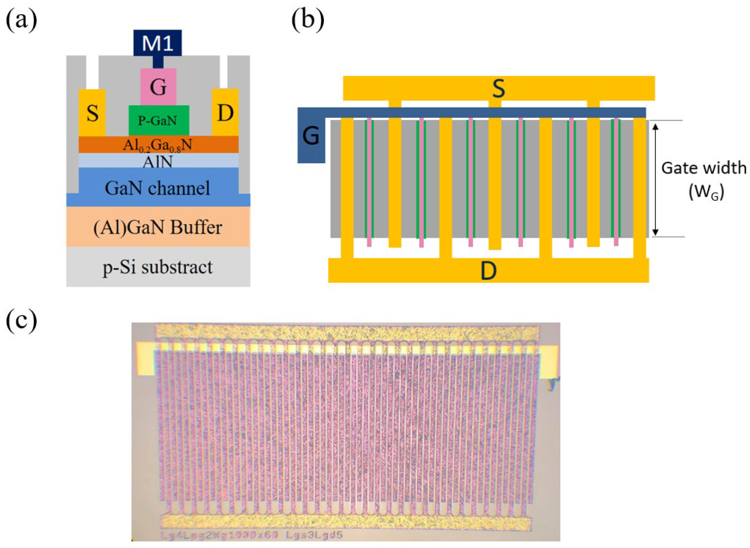
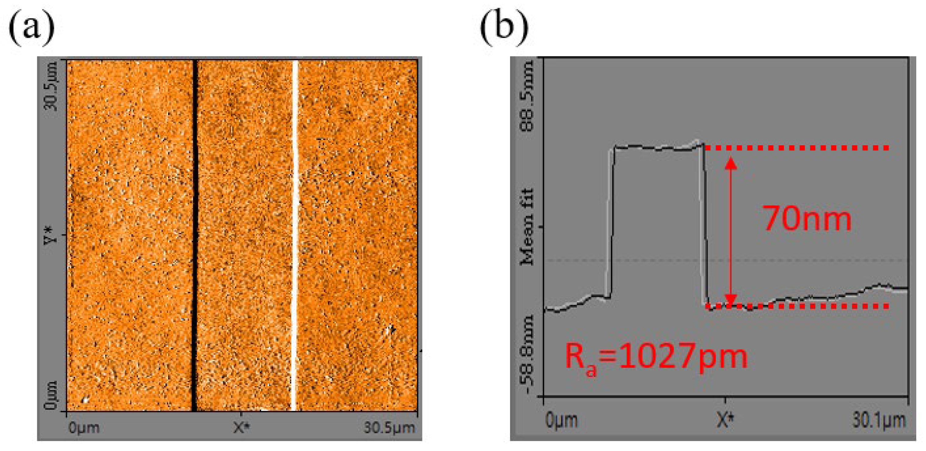
2. Materials and Methods

Figure 1a,b shows the cross-section of the p-GaN gate HEMTs and schematic top view of the p-GaN HEMT with multi-finger structure, respectively. The AlGaN/GaN heterostructures were grown by MOCVD on 800 μm p-Si substrates. The layer stack consisted of a 3.8 μm thick (Al)GaN buffer layer to enable high voltage operation, a 300 nm thick GaN channel layer, an 8 nm AlN spacer layer to effectively suppress alloy disorder scattering [29], and a 15 nm Al0.2Ga0.8N barrier layer. The top layer consisted of a 70 nm thick Mg-doped p-GaN layer with a doping concentration of 4 × 1019 cm−3.
The device fabrication started with active region isolation by mesa etching to a 200-nm depth using Cl2/BCl3 SAMCO ICP RIE-200iPC (inductively coupled plasma reactive ion etching). Then, the 7-μm long p-GaN gate region was protected using photoresist, and a high-selectivity Cl2/BCl3/SF6-mixed gas plasma etch was performed on the non-gated active region by using ICP RIE200i. In principle, when the SF6 plasma reaches the AlGaN barrier surface, the fluorine ion reacts with the Al atoms and forms a thin AlF3 etching stop layer (SF6 plasma + Al→AlF3). During the dry etching process, the employment of endpoint detection provides real-time monitoring of the etching depth where specific wavelengths of light (300–350 nm) are irradiated on the surface of the non-gated active region. After the light source reaches the surface, a portion of light is reflected directly from the surface, but some enters the wafer and is reflected back from the channel layer. Thus, the reflected light received by the detector is a combination of signals from each layer within the sample, and specific interference fringes are then formed and can be displayed on a monitor. If the etching depth does not change, the reflected light intensity would stay constant. A mixture of Cl2/BCl3/SF6 gas plasma was applied to remove the p-GaN cap for 132.8 s, and the reflected light intensity remained constant after that time indicating the end of the etching process. After that, the thin AlF3 layer on the surface was removed by a buffered oxide etchant (BOE) wet treatment for 1 min. The resulting surface and actual etching depth were measured by NanoSurf Flex atomic force microscopy (AFM) as shown in Figure 2. The etching depth was exactly 70 nm, the thickness of the p-GaN layer, and the average roughness (Ra) was 1027 pm (30 × 30 μm2). Afterwards, Ti/Al/Ni/Au (25/125/40/150 nm) were used to form ohmic contacts as source and drain electrodes, followed by annealing in N2 ambient at 875 °C for 45 s using Premtek RTP-T41M (rapid thermal processing). Using a transmission line measurement (TLM), the channel sheet resistance and specific contact resistivity were 310 Ω/sq and 9469 Ω·μm2, respectively. The good ohmic contact and sheet resistance were due to the accurate etching depth (which maintains a high 2DEG density) and smooth surface with negligible ion bombardment damage. Ni/Au (15/280 nm) gate metal was deposited by e-beam evaporation to form a Schottky contact. Next, 300 nm thick SiNx surface passivation was deposited using Samco PD-220N PECVD to reduce the N vacancies on the device’s surface. Finally, after contact window opening on the gate regions, a thick Ti/Au (15/1300 nm) Metal 1 was deposited to serve as the gate electrode bridge. The realized large-area p-GaN HEMT device with multi-finger structure is shown in Figure 1c. The power device has a gate length (LG) of 4 μm, gate–source distance (LGS) of 3 μm, gate–drain distance (LGD) of 3 μm, and total gate width of 60 mm. The device DC characteristics were analyzed using an Agilent B1505A power device analyzer.

3. Results and Discussion

In order to investigate the relationship between the output current density and multi-finger layout, p-GaN gate HEMT devices with different gate width (WG) and different number of fingers were fabricated simultaneously on the same chip. In Section 3.1, devices with single finger but different WG are compared. In Section 3.2, devices with WG = 60 μm but different number of fingers are also compared. In Section 3.3, a summary for these different layouts is discussed. Finally, in Section 3.4, a high drain current p-GaN HEMT with a multi-finger layout is realized and presented.

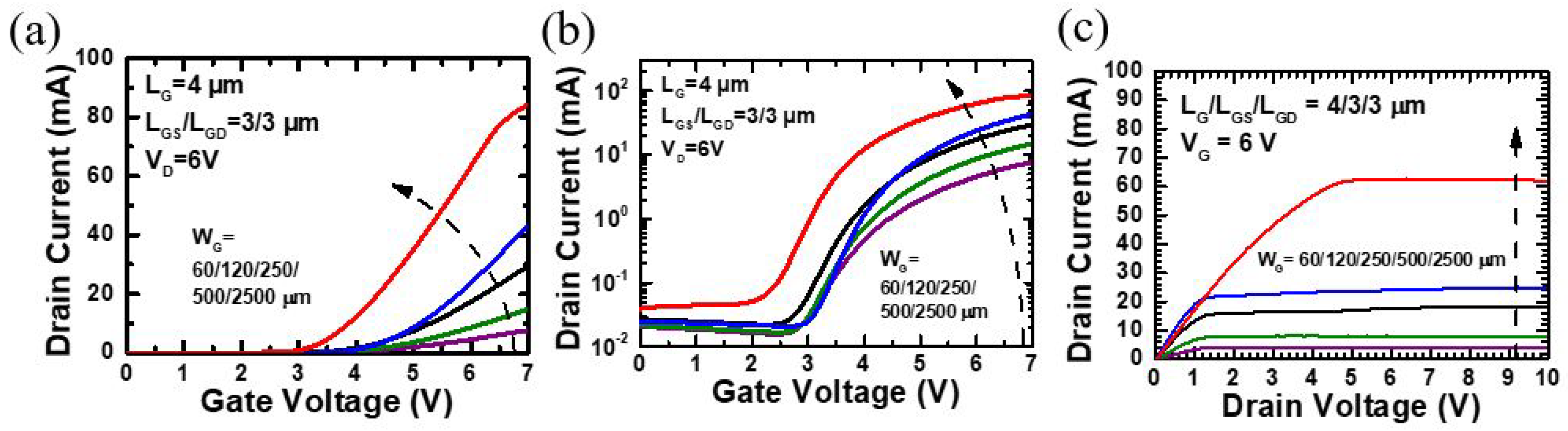
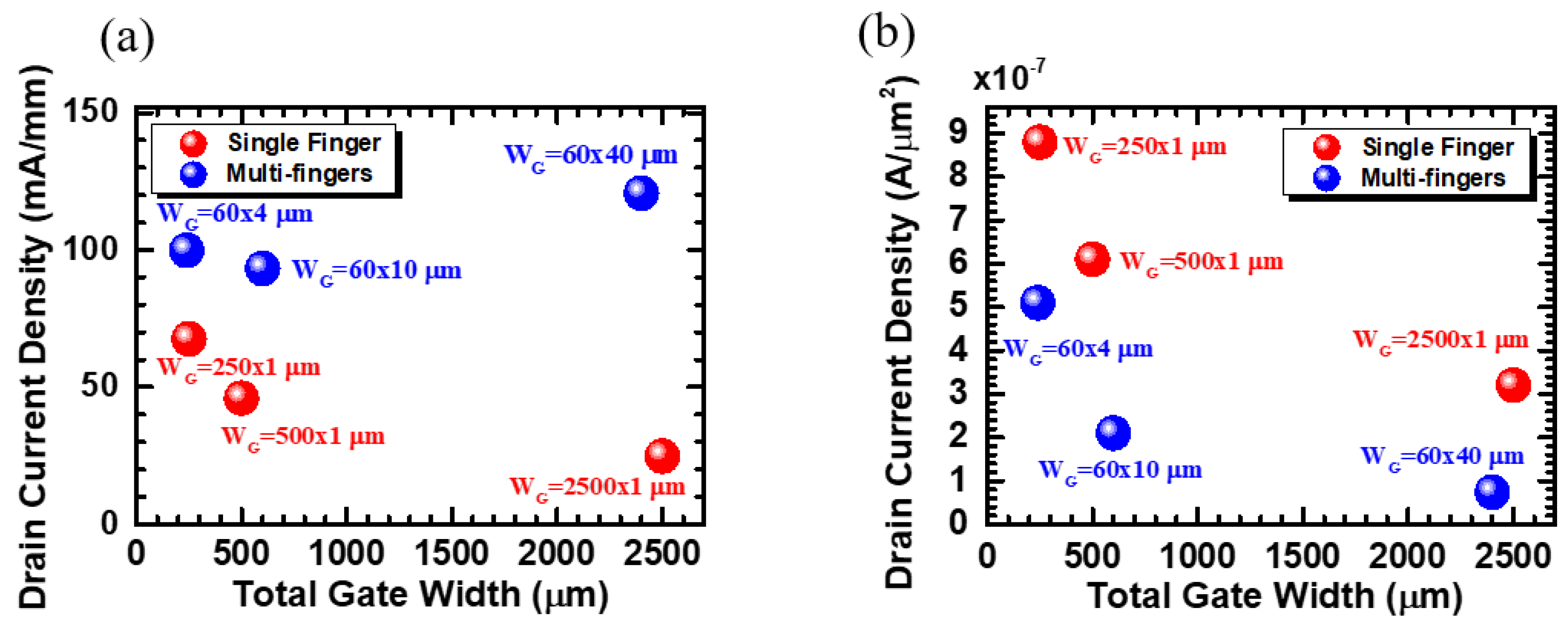
3.1. Single Finger Devices with Different WG

As shown in Table 1, five single-finger devices with different gate width are labeled as A (WG = 60 μm), B (WG = 120 μm), C (WG = 250 μm), D (WG = 500 μm), and E (WG = 2500 μm), while all other parameters (LG/LGS/LGD = 4/3/3 μm) are held constant. Figure 3a,b shows the transfer curves of different WG p-GaN HEMTs at VDS = 6 V and VGS = 0~7 V, and Figure 3c shows output performance at VGS = 6 V and VDS = 0~10 V.
As seen in Figure 3a,b, the drain current reaches 83.5 mA for device E (WG = 2500 μm) and drops to 7.4 mA for device A (WG = 60 μm). This result is consistent with the standard trend of Si-MOSFETs where the total current increases with longer gate width. However, as shown in Table 1, the current density of device A is four times greater than the current density of device E. That is to say, the current density decreases when the gate width increases. Meanwhile, according to Figure 3c, the on-resistance also dramatically drops when the gate width increases to 2500 μm. A possible reason for this tendency is that when the gate voltage is applied on the top finger region (blue gate in Figure 1b), the total voltage source cannot bias to the end of the individual gate fingers (Figure 1b green and pink gates) due to the long gate width. Thus, the gate cannot control the channel under the end of the gate finger, resulting in the 2DEG being unable to form. Table 1 summarizes the design parameters and electrical characteristics for devices with a single finger but different gate widths.

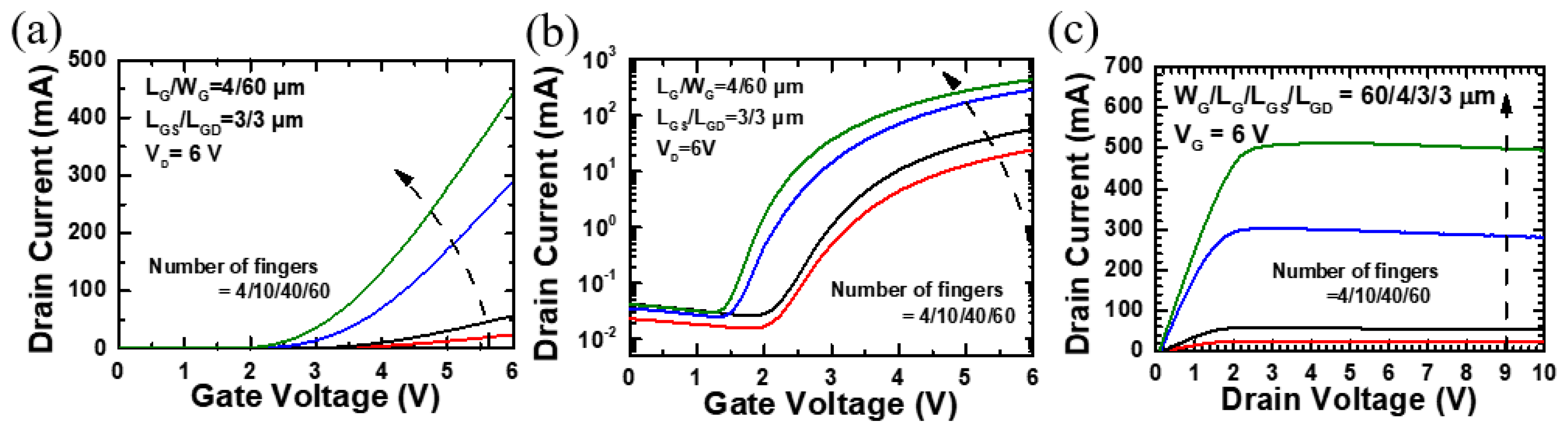
3.2. WG = 60 μm Devices with Different Number of Fingers

As presented in Table 2, four devices with the same 60 μm gate width and different number of fingers are labeled as F (4 fingers), G (10 fingers), H (40 fingers), and I (60 fingers) while all other parameters (LG/LGS/LGD = 4/3/3 μm) are held constant.
Figure 4a,b depicts the IDS-VGS transfer curves of the WG = 60 μm devices with a different number of fingers at VDS = 6 V. The output drain current at a drain bias of 6 V is 442 mA for device I (60 fingers) and 24 mA for device F (4 fingers). As shown in Table 2, the current density also increases with the number of fingers. This elevated current is due to the superposition of current from each finger. Moreover, according to Figure 4c, the rising output current results from the decrease of on-resistance from 45.68 Ω for device F (4 fingers) to 3.65 Ω for device I (60 fingers). Table 2 summarizes the design parameters and electrical characteristics for the devices with WG = 60 μm but different number of fingers.

3.3. Summary of the Multi-Finger Layout Devices

In order to compare whether the modulation of gate width or number of fingers has a greater impact on the current density, the drain current density (mA/mm) is plotted against the total gate width in Figure 5a. Thus, devices with similar total gate width are more readily compared. For example, device C and device F which have total gate widths of 250 mm and 240 mm, respectively, are compared to show that when the devices have similar total gate width, the devices with a multi-finger structure (blue) have significantly higher current density than devices with a single finger layout (red). The current is greatly increased as the total gate width is close to 2500 μm. The results are consistent with the current commercial trend which commonly applies the multi-finger structure on the devices. The drain current per active area (A/μm2) is also plotted against the total gate width, as shown in Figure 5b. The results indicate that, with a similar total gate width, the devices with a multi-finger layout (blue) have higher output current density than the devices with a single finger structure (red). This result is attributed to the thermal crosstalk between individual gate fingers which may increase device temperature and also reduce the power density [20]. Meanwhile, a larger active area brings about more heat dissipation. Thus, increasing the active area of the multi-finger devices will likely improve the drain current per active area.

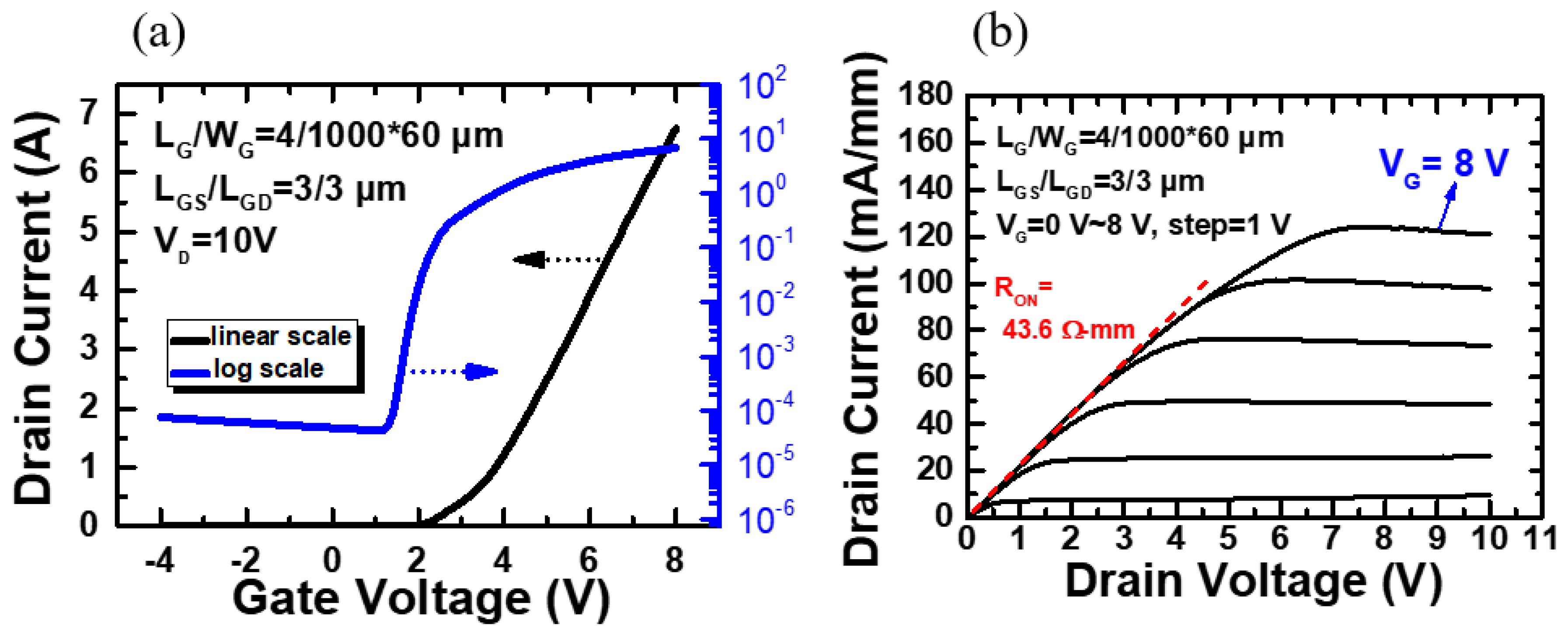
3.4. Large-Area p-GaN HEMT with High Drain Current Power Device Performance

Based on these experimental results, a high current normally-off p-GaN HEMT device was fabricated. The device is designed with a total gate width of 60 mm (WG = 1000 μm, number of fingers = 60), LG of 4 μm, LGD of 3 μm, and LGS of 3 μm. The device DC characteristics are analyzed using an Agilent B1505A power device analyzer. The transfer curves of the devices in linear and log scale are shown in Figure 6a at VDS = 10 V, and the output performance as a function of VGS is presented in Figure 6b.
The threshold voltage (VTH) is 2.2 V (defined by IDS = 1 mA/mm), the subthreshold swing (SS) is 221.1 mV/dec, and the on/off ratio is 1.4 × 10⁵ which exhibits good switching characteristics. The output drain current and current density is 6.7 A and 112.5 mA/mm, respectively, at VGS = 8 V and VDS = 10 V, and the on-resistance (Ron) is 43.6 Ω-mm at VGS = 8 V.

4. Conclusions

In this work, a high current normally-off p-GaN HEMT device with multi-finger layout was successfully fabricated using a self-terminating etching technique with Cl2/BCl3/SF6-mixed gas plasma. Several devices with different gate width and number of fingers were fabricated to investigate the effects on output current density. The drain current reaches 83.5 mA for devices with WG = 60 μm and drops to 7.4 mA for devices with WG = 2500 μm. The decrease in current for long gate widths is due to the fact that the applied gate voltage on the top of the gate finger cannot bias to the end of the finger, resulting in the 2DEG being unable to form. Through modulating the number of fingers, the output drain current is 442 mA for devices with 60 fingers while only 24 mA for devices with four fingers. This elevated current is due to the superposition of current from each finger. Lastly, a high current normally-off WG = 60 mm p-GaN HEMT device was realized with a threshold voltage of 2.2 V and drain current of 6.7 A.

Author Contributions

Conceptualization and methodology, C.-H.W., Y.-L.H. and Y.-C.C.; device process and data analysis, Y.-L.H., Y.-C.C., and T.-Y.H.; manuscript writing, Y.-C.C., and T.-Y.H.; supervision, C.-H.W., and D.-W.H.; project administration, C.-H.W. All authors have read and agreed to the published version of the manuscript.

Funding

This research was funded by the Ministry of Science and Technology of Taiwan (grant number: MOST 109-2622-8002-003, 109-2224-E992-001, 109-2221-E002-183-MY2, 109-2218-E005-012, and 109-2622-E002-020-CC2) and was also supported by the National Chung-Shan Institute of Science & Technology, R.O.C., under the grant NO. NCSIST-301-V207(109) and NO. NCSIST-403-V307(110).

Acknowledgments

The authors are grateful for the research support provided by Wen-Ta Hsu and An-Jye Tzou at Taiwan Semiconductor Research Institute (TSRI). And we are also grateful for the research support provided by the National Chung-Shan Institute of Science & Technology, R.O.C., under the grant NO. NCSIST-301-V207(109) and NO. NCSIST-403-V307(110).

Conflicts of Interest

The authors declare no conflict of interest.

References

  1. Ding, X.; Zhou, Y.; Cheng, J. A review of gallium nitride power device and its applications in motor drive. CES Trans. Electr. Mach. Syst. 2019, 3, 54–64. [Google Scholar] [CrossRef]
  2. Millan, J.; Godignon, P.; Perpina, X.; Perez-Tomas, A.; Rebollo, J. A Survey of Wide Bandgap Power Semiconductor Devices. IEEE Trans. Power Electron. 2014, 29, 2155–2163. [Google Scholar] [CrossRef]
  3. Chen, K.J.; Haberlen, O.; Lidow, A.; Tsai, C.L.; Ueda, T.; Uemoto, Y.; Wu, Y. GaN-on-Si Power Technology: Devices and Applications. IEEE Trans. Electron Devices 2017, 64, 779–795. [Google Scholar] [CrossRef]
  4. Wu, Y.-F.; Gritters, J.; Shen, L.; Smith, R.P.; Swenson, B. kV-Class GaN-on-Si HEMTs Enabling 99% Efficiency Converter at 800 V and 100 kHz. IEEE Trans. Power Electron. 2014, 29, 2634–2637. [Google Scholar] [CrossRef]
  5. Meneghesso, G.; Meneghini, M.; Zanoni, E. Breakdown mechanisms in AlGaN/GaN HEMTs: An overview. Jpn. J. Appl. Phys. 2014, 53, 100211. [Google Scholar] [CrossRef]
  6. Cai, Y.; Zhou, Y.; Chen, K.J.; Lau, K.M. High-performance enhancement-mode AlGaN/GaN HEMTs using fluoride-based plasma treatment. IEEE Electron Device Lett. 2005, 26, 435–437. [Google Scholar] [CrossRef]
  7. Chu, R.; Corrion, A.; Chen, M.; Li, R.; Wong, D.; Zehnder, D.; Hughes, B.; Boutros, K. 1200-V Normally Off GaN-on-Si Field-Effect Transistors With Low Dynamic on -Resistance. IEEE Electron Device Lett. 2011, 32, 632–634. [Google Scholar] [CrossRef]
  8. Lee, C.-H.; Lin, W.-R.; Lee, Y.-H.; Huang, J.-J. Characterizations of Enhancement-Mode Double Heterostructure GaN HEMTs With Gate Field Plates. IEEE Trans. Electron Devices 2018, 65, 488–492. [Google Scholar] [CrossRef]
  9. Cai, Y.; Zhou, Y.; Lau, K.M.; Chen, K.J. Control of Threshold Voltage of AlGaN/GaN HEMTs by Fluoride-Based Plasma Treatment: From Depletion Mode to Enhancement Mode. IEEE Trans. Electron Devices 2006, 53, 2207–2215. [Google Scholar] [CrossRef]
  10. Huang, S.; Liu, X.; Wang, X.; Kang, X.; Zhang, J.; Fan, J.; Shi, J.; Wei, K.; Zheng, Y.; Gao, H.; et al. Ultrathin-Barrier AlGaN/GaN Heterostructure: A Recess-Free Technology for Manufacturing High-Performance GaN-on-Si Power Devices. IEEE Trans. Electron Devices 2018, 65, 207–214. [Google Scholar] [CrossRef]
  11. Saito, W.; Takada, Y.; Kuraguchi, M.; Tsuda, K.; Omura, I. Recessed-gate structure approach toward normally off high-Voltage AlGaN/GaN HEMT for power electronics applications. IEEE Trans. Electron Devices 2006, 53, 356–362. [Google Scholar] [CrossRef]
  12. Uemoto, Y.; Hikita, M.; Ueno, H.; Matsuo, H.; Ishida, H.; Yanagihara, M.; Ueda, T.; Tanaka, T.; Ueda, D. Gate Injection Transistor (GIT)—A Normally-Off AlGaN/GaN Power Transistor Using Conductivity Modulation. IEEE Trans. Electron Devices 2007, 54, 3393–3399. [Google Scholar] [CrossRef]
  13. Wang, H.; Wei, J.; Xie, R.; Liu, C.; Tang, G.; Chen, K.J. Maximizing the Performance of 650-V p-GaN Gate HEMTs: Dynamic RON Characterization and Circuit Design Considerations. IEEE Trans. Power Electronics 2017, 32, 5539–5549. [Google Scholar] [CrossRef]
  14. Tang, X.; Li, B.; Amini, H.; Tanner, P.; Han, J.; Dimitrijev, S. Mechanism of Threshold Voltage Shift in p -GaN Gate AlGaN/GaN Transistors. IEEE Electron Device Lett. 2018, 39. [Google Scholar] [CrossRef]
  15. Suzuki, Y.; Tone, K.; Asubar, J.T.; Tokuda, H.; Kuzuhara, M. High drain current and low on-resistance in AlGaN/GaN HEMTs with Au-plated ohmic electrodes. In Proceedings of the 2015 IEEE International Meeting for Future of Electron Devices, Kansai (IMFEDK), Kyoto, Japan, 4–5 June 2015; pp. 52–53. [Google Scholar]
  16. Zhang, N.; Mehrotra, V.; Chandrasekaran, S.; Moran, B.; Shen, L.; Mishra, U.; Etzkorn, E.; Clarke, D. Large area GaN HEMT power devices for power electronic applications: Switching and temperature characteristics. In Proceedings of the IEEE 34th Annual Conference on Power Electronics Specialist, PESC ’03, Acapulco, Mexico, 15–19 June 2003. [Google Scholar]
  17. Reiner, R.; Waltereit, P.; Benkhelifa, F.; Muller, S.; Wespel, M.; Quay, R.; Schlechtweg, M.; Mikulla, M.; Ambacher, O. Benchmarking of Large-Area GaN-on-Si HFET Power Devices for Highly-Efficient, Fast-Switching Converter Applications. In Proceedings of the 2013 IEEE Compound Semiconductor Integrated Circuit Symposium (CSICS), Monterey, CA, USA, 13–16 October 2013. [Google Scholar]
  18. Posthuma, N.; You, S.; Liang, H.; Ronchi, N.; Kang, X.; Wellekens, D.; Saripalli, Y.; Decoutere, S. Impact of Mg out-diffusion and activation on the p-GaN gate HEMT device performance. In Proceedings of the 2016 28th International Symposium on Power Semiconductor Devices and ICs (ISPSD), Prague, Czech Republic, 12–16 June 2016; pp. 95–98. [Google Scholar]
  19. Xin, X.; Shi, J.; Liu, L.; Edwards, J.; Swaminathan, K.; Pabisz, M.; Murphy, M.; Eastman, L.F.; Pophristic, M. Demonstration of low-leakage-current low-on-resistance 600-V 5.5-A GaN/AlGaN HEMT. IEEE Electron Device Lett. 2009, 30, 1027–1029. [Google Scholar]
  20. Chvála, A.; Marek, J.; Príbytný, P.; Šatka, A.; Stoffels, S.; Posthuma, N.; Decoutere, S.; Donoval, D. Analysis of multifinger power HEMTs supported by effective 3-D device electrothermal simulation. Microelectron. Reliab. 2017, 78, 148–155. [Google Scholar] [CrossRef]
  21. Lukens, G.; Hahn, H.; Kalisch, H.; Vescan, A. Self-Aligned Process for Selectively Etched p-GaN-Gated AlGaN/GaN-on-Si HFETs. IEEE Trans/ Electron Devices 2018, 65, 3732–3738. [Google Scholar] [CrossRef]
  22. Chiu, H.-C.; Chang, Y.-S.; Li, B.-H.; Wang, H.-C.; Kao, H.-L.; Chien, F.-T.; Hu, C.-W.; Xuan, R. High Uniformity Normally-OFF p-GaN Gate HEMT Using Self-Terminated Digital Etching Technique. IEEE Trans. Electron Devices 2018, 65, 4820–4825. [Google Scholar] [CrossRef]
  23. Burnham, S.D.; Boutros, K.; Hashimoto, P.; Butler, C.; Wong, D.W.S.; Hu, M.; Micovic, M. Gate-recessed normally-off GaN-on- Si HEMT using a new O2-BCl3 digital etching technique. Phys. Status Solidi C 2010, 7, 2010–2012. [Google Scholar] [CrossRef]
  24. Lin, Y.; Lin, Y.C.; Lumbantoruan, F.; Dec, C.F.; Majilis, B.Y.; Chang, E.Y. A Novel Digital Etch Technique for p-GaN Gate HEMT. In Proceedings of the 2018 IEEE International Conference on Semiconductor Electronics (ICSE), Kuala Lumpur, Malaysia, 15–17 August 2018. [Google Scholar]
  25. Hahn, H.; Lükens, G.; Ketteniss, N.; Kalisch, H.; Vescan, A. Recessed-Gate Enhancement-Mode AlGaN/GaN Heterostructure Field-Effect Transistors on Si with Record DC Performance. Appl. Phys. Express 2011, 4, 114102. [Google Scholar] [CrossRef]
  26. Green, R.T.; Luxmoore, I.J.; Lee, K.B.; Houston, P.A.; Ranalli, F.; Wang, T.; Parbrook, P.J.; Uren, M.J.; Wallis, D.J.; Martin, T. Characterization of gate recessed GaN/AlGaN/GaN high electron mobility transistors fabricated using a SiCl4/SF6 dry etch recipe. J. Appl. Phys. 2010, 108, 013711. [Google Scholar] [CrossRef]
  27. Wong, J.C.; Micovic, M.; Brown, D.F.; Khalaf, I.; Williams, A.; Corrion, A. Selective anisotropic etching of GaN over AlGaN for very thin films. J. Vac. Sci. Technol A Vac. Surfaces Films 2018, 36, 030603. [Google Scholar] [CrossRef]
  28. Zhou, S.; Cao, B.; Liu, S. Dry etching characteristics of GaN using Cl2/BCl3 inductively coupled plasmas. Appl. Surface Sci. 2010, 257, 905–910. [Google Scholar] [CrossRef]
  29. Tülek, R.; Ilgaz, A.; Gökden, S.; Teke, A.; Öztürk, M.K.; Kasap, M.; Özçelik, S.; Arslan, E.; Özbay, E. Comparison of the transport properties of high quality AlGaN/AlN/GaN and AlInN/AlN/GaN two-dimensional electron gas heterostructures. J. Appl. Phys. 2009, 105, 013707. [Google Scholar] [CrossRef] [Green Version]
Figure 1. (a) Cross section of the p-gallium nitride (GaN) high electron mobility transistors (HEMT) device structure. (b) Schematic top view of the p-GaN HEMT device structure. (c) Optical micrograph of a realized p-GaN gate HEMT (individual gate width WG/# of fingers = 1000 μm/60, LG = 4 μm, LGD = 3 μm, and LGS = 3 μm).
Micromachines 12 00432 g001
Figure 2. (a) Atomic force microscopy (AFM) image of the p-GaN gate region. (b) The depth profile of the p-GaN gate with an etching depth 70 nm and average roughness (Ra) of 1027 pm.
Micromachines 12 00432 g002
Figure 3. Device performance of single finger p-GaN HEMTs with different gate width (60/120/250/500/2500 μm) at VDS = 6 V: (a) IDS-VGS in linear scale, (b) IDS-VGS in log scale, (c) and output characteristics.
Micromachines 12 00432 g003
Figure 4. Device performance of p-GaN HEMTs (WG = 60 μm) with different number of fingers (4/10/40/60) at VDS = 6 V: (a) IDS-VGS in linear scale, (b) IDS-VGS in log scale, (c) and output characteristics.
Micromachines 12 00432 g004
Figure 5. Drain current densities of p-GaN HEMTs with different total gate width. (a) Drain current density (normalized by WG) versus total gate width. (b) Drain current density (normalized by active area) versus total gate width.
Micromachines 12 00432 g005
Figure 6. Device performance of the large-area p-GaN HEMT with total gate width 60 mm (1000 mm × 60 fingers). (a) Total drain current versus gate voltage at VDS = 10 V in linear and log scale. (b) Output performance at VDS = 0–10 V and VGS = 0–8 V.
Micromachines 12 00432 g006
Table 1. Design parameters for single finger devices with different gate widths (WG).
DevicesABCDE
Total gate width (μm)601202505002500
Single WG (μm)601202505002500
# of fingers11111
Active area (μm2)4560912019,00038,000190,000
IDS,on (mA/mm)73.3969.73567.60846.01224.875
IDS,on (mA/μm2)9.7 × 1049.2 × 1048.8 × 1046.1 × 1043.2 × 104
Table 2. Design parameters for WG = 60 μm devices with different number of fingers.
DevicesFGHI
Total gate width (μm)24060024003600
Single WG (μm)60606060
# of fingers4104060
Active area (μm2)11,76036,16098,160146,160
IDS,on (mA/mm)99.8793.29120.7140.56
IDS,on (mA/μm2)5.1 × 1042.1 × 1047.4 × 1055.8 × 105
Publisher’s Note: MDPI stays neutral with regard to jurisdictional claims in published maps and institutional affiliations.

