Simulation Study of Surface Transfer Doping of Hydrogenated Diamond by MoO3 and V2O5 Metal Oxides


Abstract
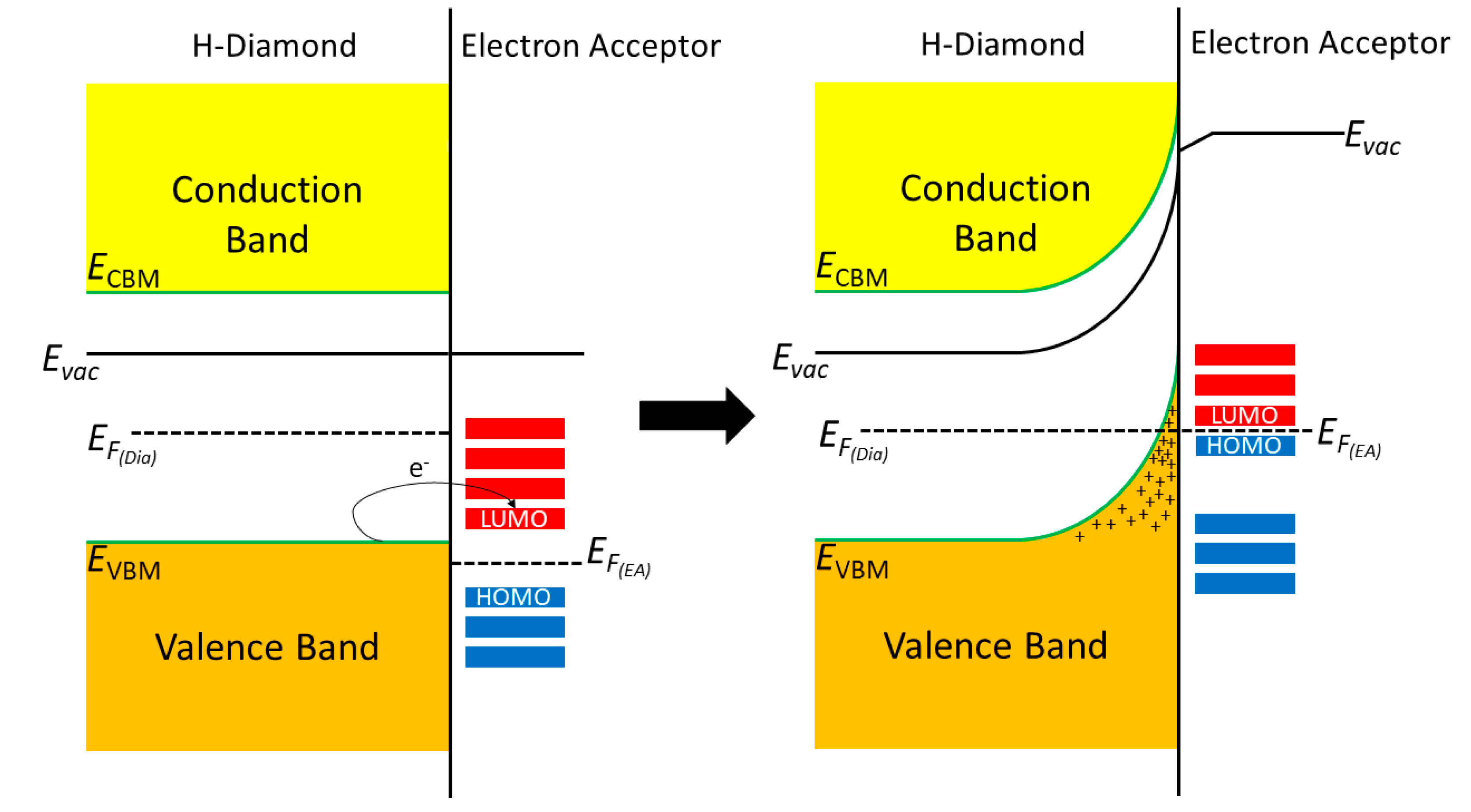
1. Introduction
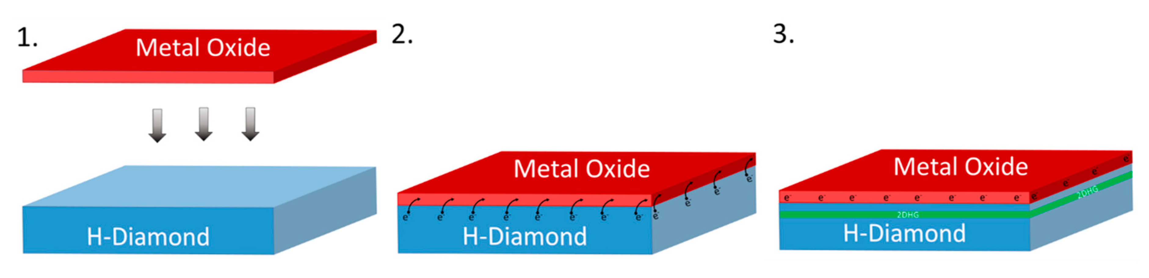
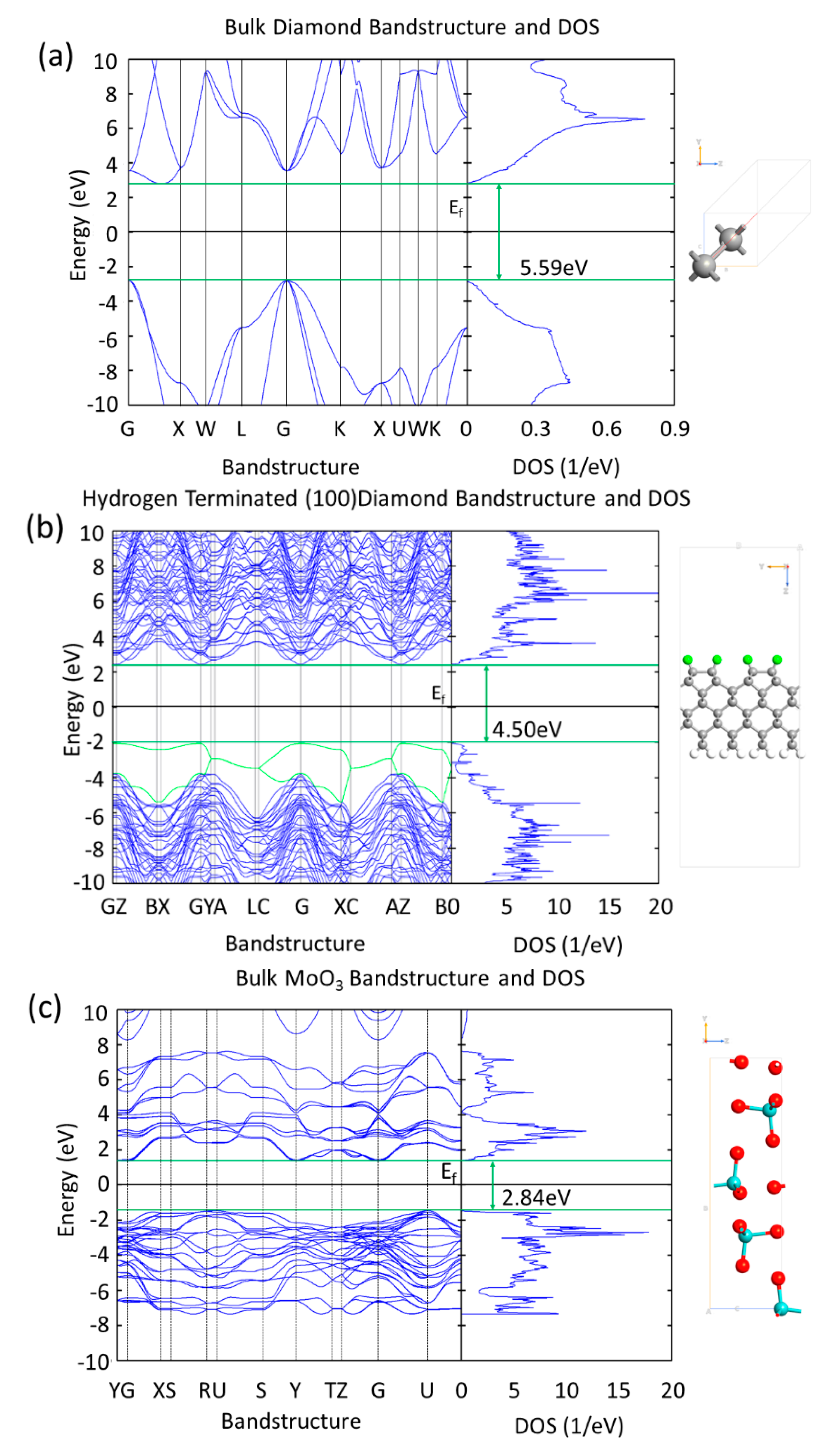
2. Materials and Methods
3. Results
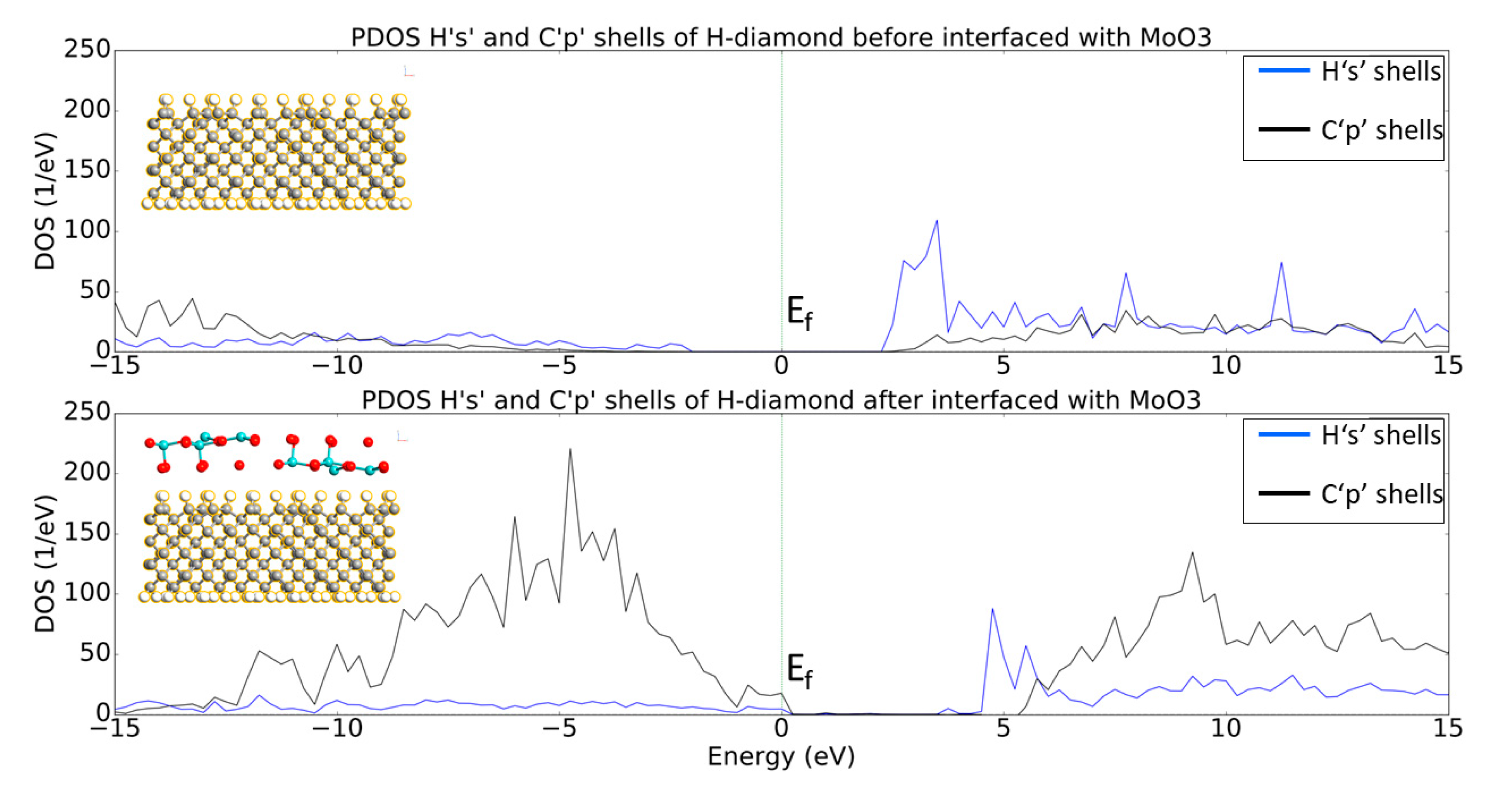
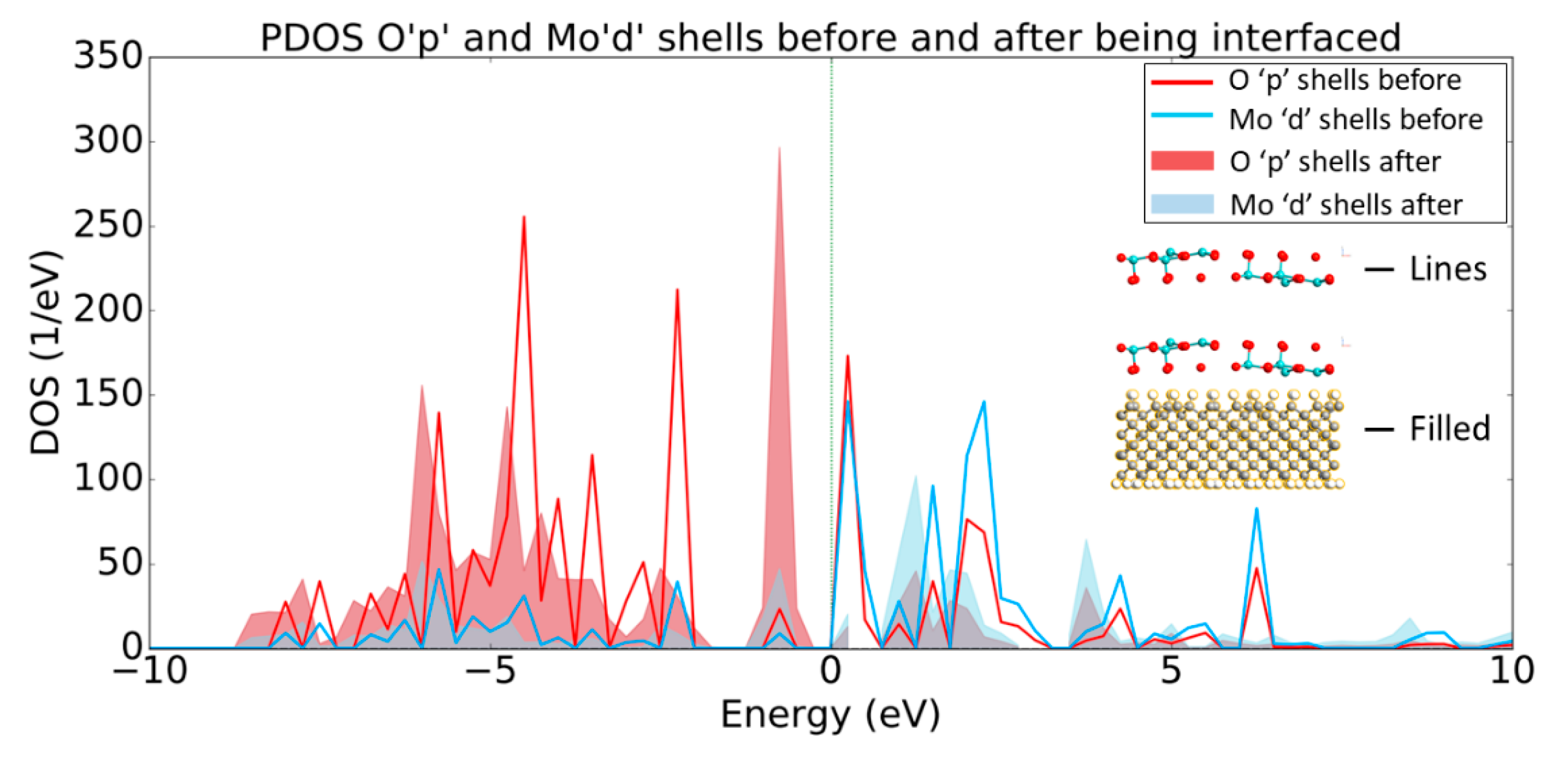
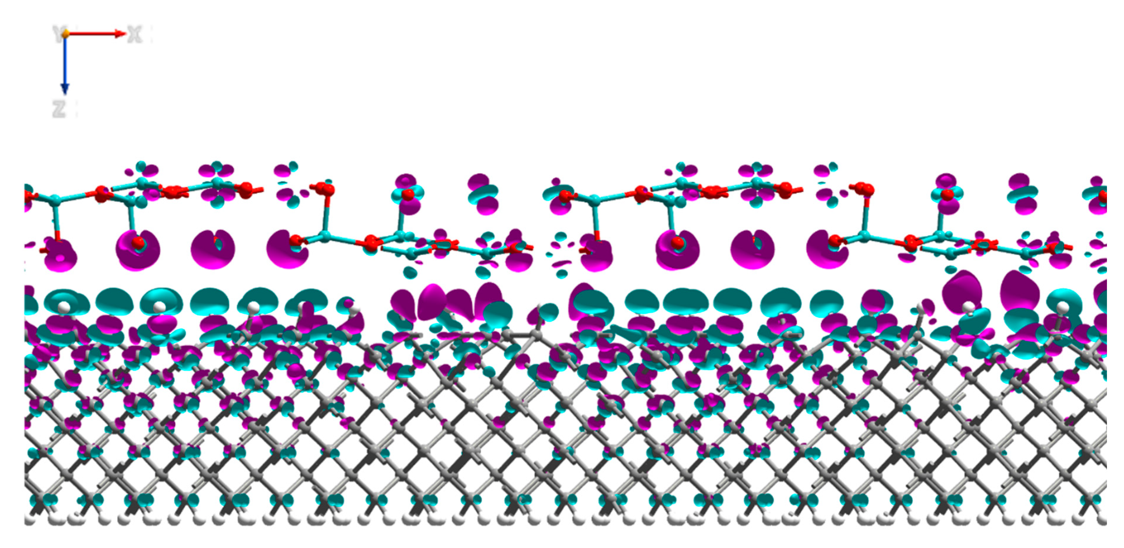
3.1. MoO3: H-Diamond Interface
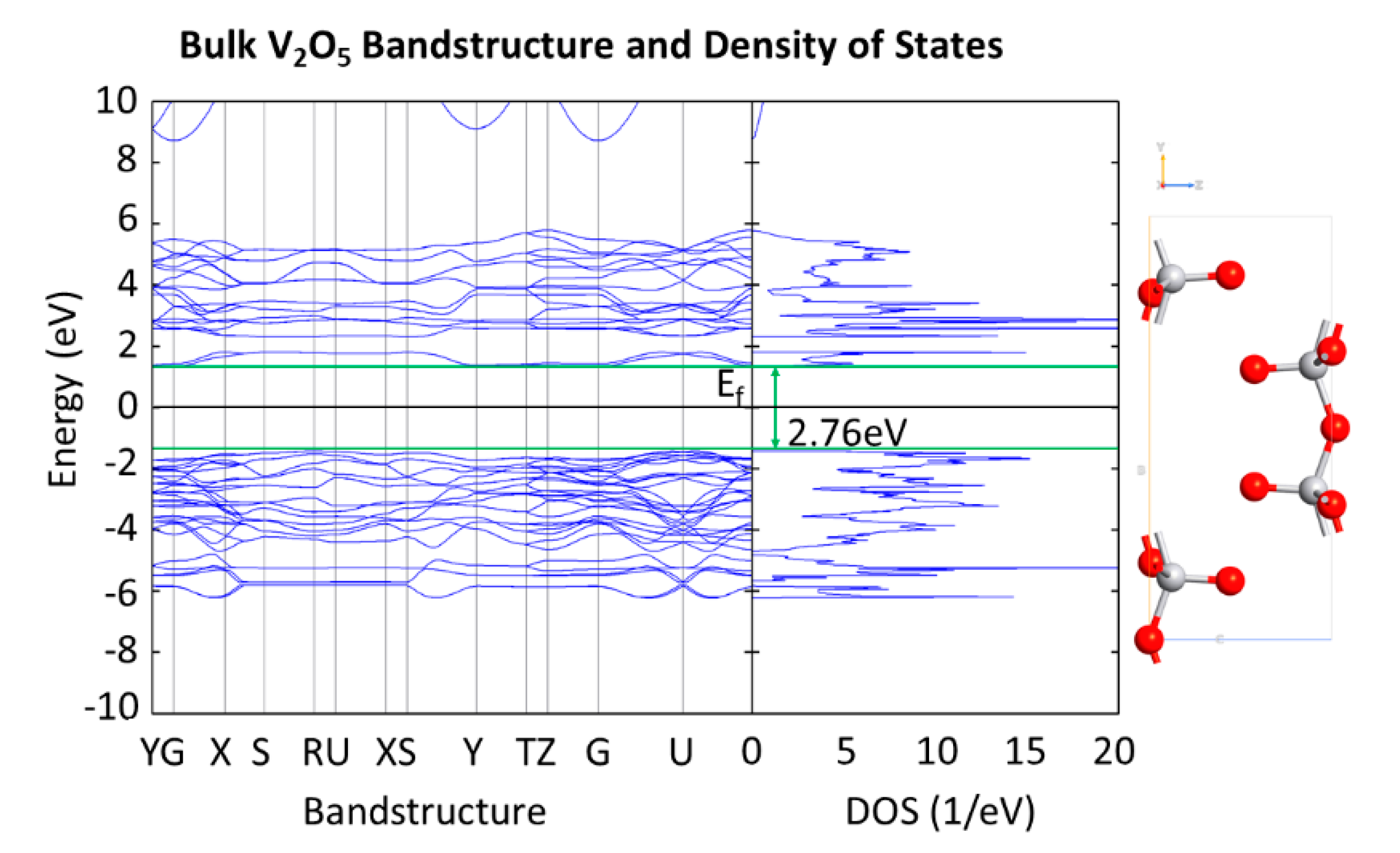
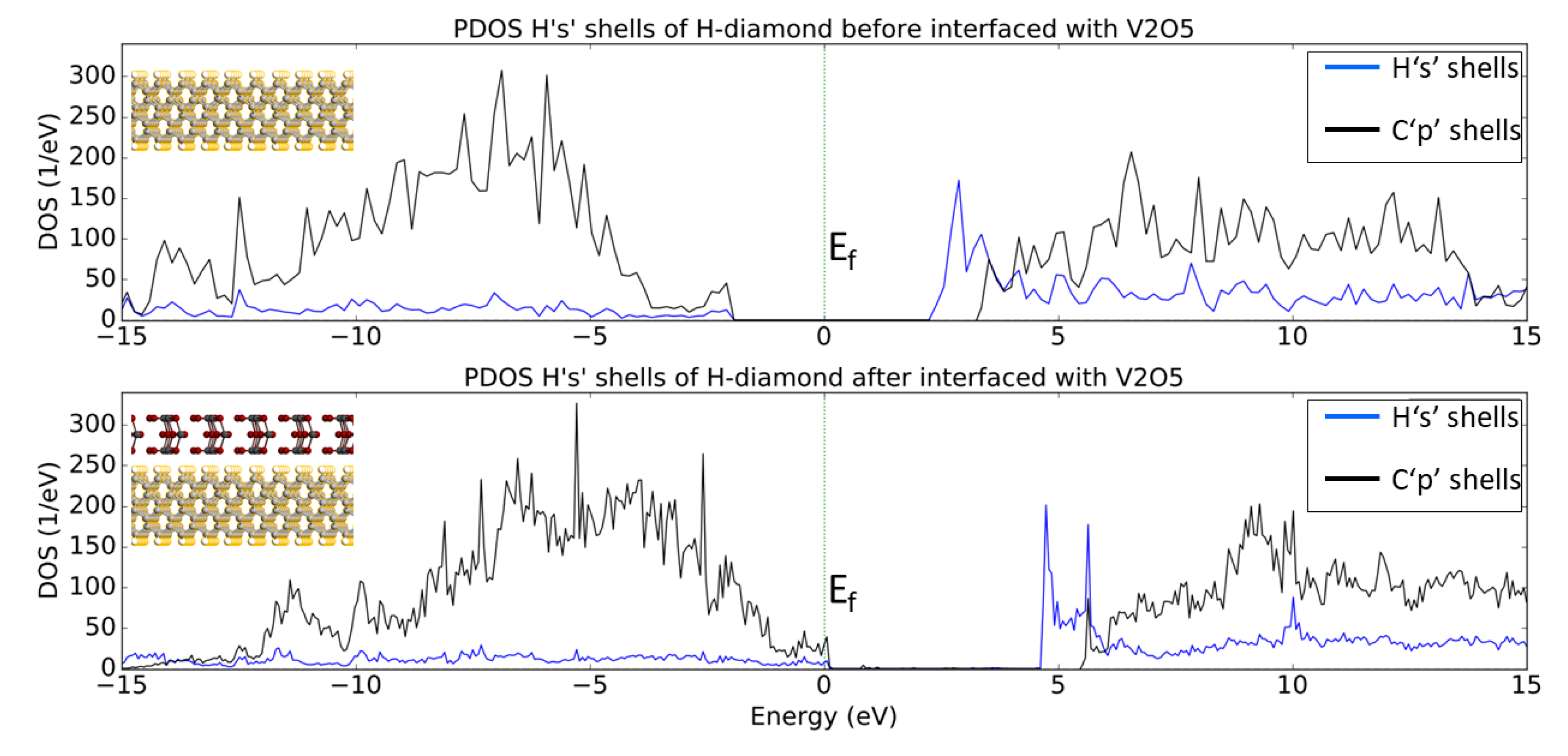
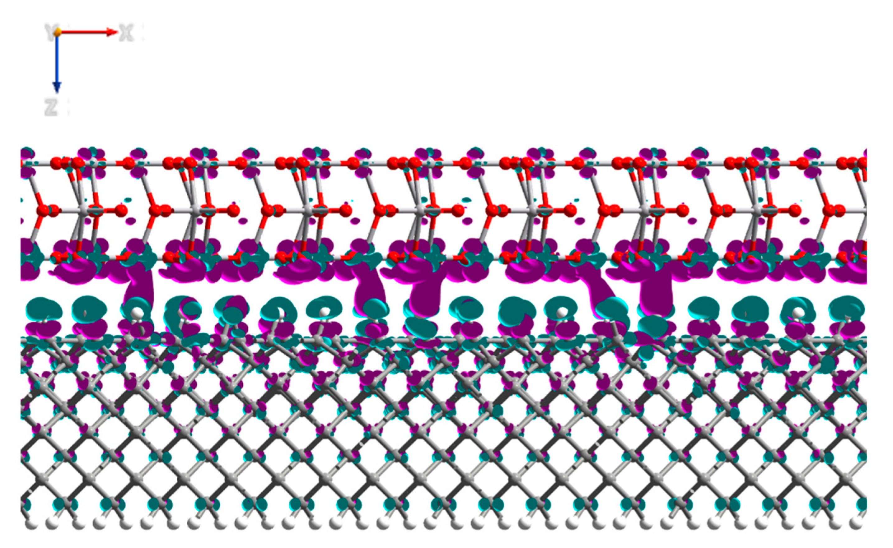
3.2. V2O5: H-Diamond Interface
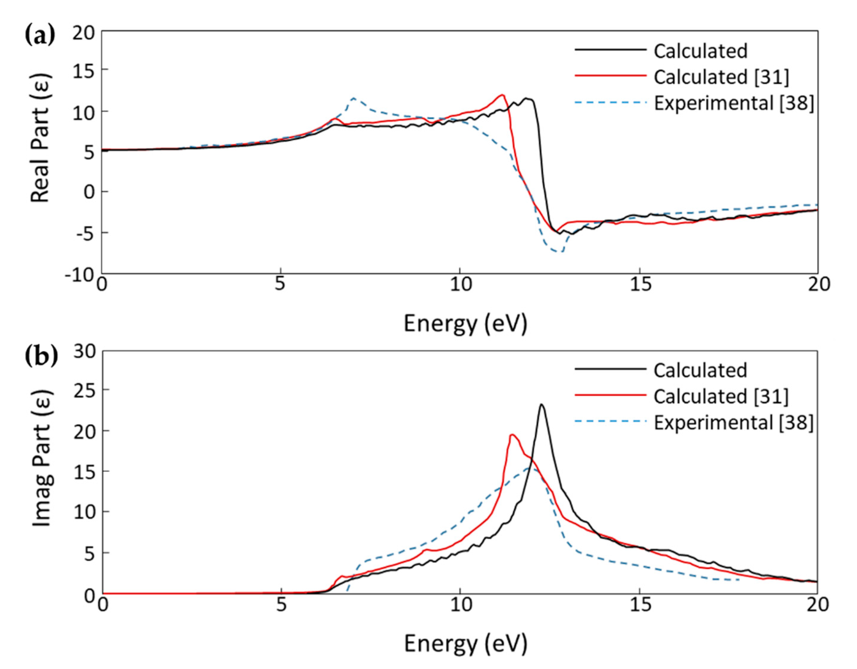
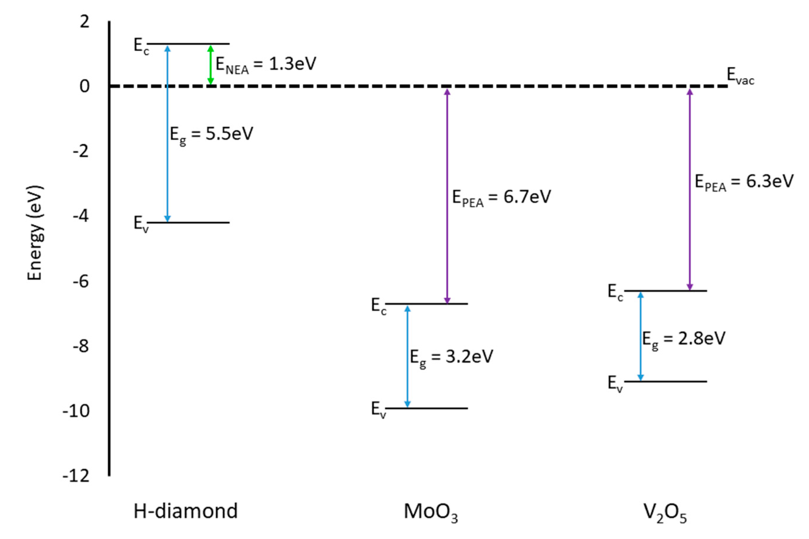
3.3. MoO3 and V2O5 Comparison
4. Discussion
Author Contributions
Funding
Acknowledgments
Conflicts of Interest
References
- Trew, R.J.; Yan, J.; Mock, P.M. The potential of diamond and SiC electronic devices for microwave and millimeter-wave power applications. Proc. IEEE 1991, 79, 598–620. [Google Scholar] [CrossRef]
- Willander, M.; Friesel, M.; Wahab, Q.-U.; Straumal, B. Silicon carbide and diamond for high temperature device applications. J. Mater. Sci. Mater. Electron. 2006, 17, 1. [Google Scholar] [CrossRef]
- Wort, C.; Balmer, R. Diamond as an Electronic material. Mater. Today 2008, 11, 22–28. [Google Scholar] [CrossRef]
- Liu, J.; Ohsato, H.; Wang, X.; Liao, M.; Koide, Y. Design and fabrication of high-performance diamond triple-gate field-effect transistors. Sci. Rep. 2016, 6, 34757. [Google Scholar] [CrossRef] [PubMed]
- Russell, S.; Sharabi, S.; Tallaire, A.; Moran, D.A.J. RF Operation of Hydrogen-Terminated Diamond Field Effect Transistors. IEEE 2015, 62, 751–756. [Google Scholar]
- Kitabayashi, Y.; Kudo, T.; Tsuboi, H.; Yamada, T.; Xu, D.; Shibata, M.; Matsumura, D.; Hayashi, Y.; Syamsul, M.; Inaba, M.; et al. Normally-Off C–H Diamond MOSFETs With Partial C–O Channel Achieving 2-kV Breakdown Voltage. IEEE Electron Device Lett. 2017, 38, 363–366. [Google Scholar] [CrossRef]
- Isberg, J. Diamond Electronic Devices. AIP Conf. Proc. 2010, 1292, 123–128. [Google Scholar] [CrossRef]
- Hirama, K.; Takayanagi, H.; Yamauchi, S.; Jingu, Y.; Umezawa, H.; Kawarada, H. High-performance p-channel diamond MOSFETs with alumina gate insulator. In Proceedings of the 2007 IEEE International Electron Devices Meeting, Washington, DC, USA, 10–12 December 2007; pp. 873–876. [Google Scholar]
- Kawarada, H.; Yamada, T.; Xu, D.; Tsuboi, H.; Kitabayashi, Y.; Matsumura, D.; Shibata, M.; Kudo, T.; Inaba, M.; Hiraiwa, A. Durability-enhanced two-dimensional hole gas of C-H diamond surface for complementary power inverter applications. Sci. Rep. 2017, 7, 42368. [Google Scholar] [CrossRef]
- Zhou, D.; Krauss, A.R.; Qin, L.C.; McCauley, T.G.; Gruen, D.M.; Corrigan, T.D.; Chang, R.P.H.; Gnaser, H. Synthesis and electron field emission of nanocrystalline diamond thin films grown from N2/CH4 microwave plasmas. J. Appl. Phys. 1997, 82, 4546–4550. [Google Scholar] [CrossRef]
- Yokoya, T.; Nakamura, T.; Matsushita, T.; Muro, T.; Takano, Y.; Nagao, M.; Takenouchi, T.; Kawarada, H.; Oguchi, T. Origin of the metallic properties of heavily boron-doped superconducting diamond. Nature 2005, 438, 647. [Google Scholar] [CrossRef]
- Ekimov, E.A.; Sidorov, V.A.; Bauer, E.D.; Mel’nik, N.N.; Curro, N.J.; Thompson, J.D.; Stishov, S.M. Superconductivity in diamond. Nature 2004, 428, 542. [Google Scholar] [CrossRef]
- Crawford, K.G.; Cao, L.; Qi, D.; Tallaire, A.; Limiti, E.; Verona, C.; Wee, A.T.S.; Moran, D.A.J. Enhanced surface transfer doping of diamond by V2O5 with improved thermal stability. Appl. Phys. Lett. 2016, 108, 042103. [Google Scholar] [CrossRef]
- Ren, Z.; Zhang, J.; Zhang, J.; Zhang, C.; Yang, P.; Chen, D.; Li, Y.; Hao, Y. Research on the hydrogen terminated single crystal diamond MOSFET with MoO3 dielectric and gold gate metal. J. Semicond. 2018, 39, 074003. [Google Scholar] [CrossRef]
- Maier, F.; Riedel, M.; Mantel, B.; Ristein, J.; Ley, L. Origin of Surface Conductivity in Diamond. Phys. Rev. Lett. 2000, 85, 16. [Google Scholar] [CrossRef] [PubMed]
- Strobel, P.; Riedel, M.; Ristein, J.; Ley, L. Surface transfer doping of diamond. Nature 2004, 430, 439–441. [Google Scholar] [CrossRef]
- Strobel, P.; Riedel, M.; Ristein, J.; Ley, L.; Boltalina, O. Surface transfer doping of diamond by fullerene. Diam. Relat. Mater. 2005, 14, 451–458. [Google Scholar] [CrossRef]
- Edmonds, M.T.; Wanke, M.; Tadich, A.; Vulling, H.M.; Rietwyk, K.J.; Sharp, P.L.; Stark, C.B.; Smets, Y.; Schenk, A.; Wu, Q.H.; et al. Surface transfer doping of hydrogen-terminated diamond by C60F48: Energy level scheme and doping efficiency. J. Chem. Phys. 2012, 136, 124701. [Google Scholar] [CrossRef] [PubMed]
- Qi, D.; Chen, W.; Gao, X.; Wang, L.; Chen, S.; Loh, K.P.; Wee, A.T.S. Surface Transfer Doping of Diamond (100) by Tetrafluoro-tetracyanoquinodimethane. J. Am. Chem. Soc. 2007, 129, 8084–8085. [Google Scholar] [CrossRef]
- Russell, S.; Cao, L.; Qi, D.; Tallaire, A.; Crawford, K.; Wee, A.; Moran, D.A.J. Surface transfer doping of diamond by MoO3: A combined spectroscopic and Hall measurement study. Appl. Phys. Lett. 2013, 103, 20. [Google Scholar] [CrossRef]
- Vardi, A.; Tordjman, M.; Alamo, J.A.d.; Kalish, R. A Diamond:H/MoO3MOSFET. IEEE Electron Device Lett. 2014, 35, 1320–1322. [Google Scholar] [CrossRef]
- Tordjman, M.; Saguy, C.; Bolker, A.; Kalish, R. Superior Surface Transfer Doping of Diamond with MoO3. Adv. Mater. Interfaces 2014, 1, 1300155. [Google Scholar] [CrossRef]
- Colangeli, S.; Verona, C.; Ciccognani, W.; Marinelli, M.; Rinati, G.V.; Limiti, E.; Benetti, M.; Cannata, D.; Pietrantonio, F.D. H-Terminated Diamond MISFETs with V2O5 as Insulator. In Proceedings of the 2016 IEEE Compound Semiconductor Integrated Circuit Symposium (CSICS), Austin, TX, USA, 23–26 October 2016; pp. 1–4. [Google Scholar]
- Verona, C.; Arciprete, F.; Foffi, M.; Limiti, E.; Marinelli, M.; Placidi, E.; Prestopino, G.; Rinati, G.V. Influence of surface crystal-orientation on transfer doping of V2O5/H-terminated diamond. Appl. Phys. Lett. 2018, 112, 181602. [Google Scholar] [CrossRef]
- Verona, C.; Ciccognani, W.; Colangeli, S.; Limiti, E.; Marinelli, M.; Verona-Rinati, G. Comparative investigation of surface transfer doping of hydrogen terminated diamond by high electron affinity insulators. J. Appl. Phys. 2016, 120, 025104. [Google Scholar] [CrossRef]
- Crawford, K.G.; Qi, D.; McGlynn, J.; Ivanov, T.G.; Shah, P.B.; Weil, J.; Tallaire, A.; Ganin, A.Y.; Moran, D.A.J. Thermally Stable, High Performance Transfer Doping of Diamond using Transition Metal Oxides. Sci. Rep. 2018, 8, 3342. [Google Scholar] [CrossRef] [PubMed]
- Xing, K.; Xiang, Y.; Jiang, M.; Creedon, D.L.; Akhgar, G.; Yianni, S.A.; Xiao, H.; Ley, L.; Stacey, A.; McCallum, J.C.; et al. MoO3 induces p-type surface conductivity by surface transfer doping in diamond. Appl. Surf. Sci. 2020, 509, 144890. [Google Scholar] [CrossRef]
- Young, H.X.; Yu, Y.; Xu, L.F.; Gu, C.Z. Ab initio study of molecular adsorption on hydrogenated diamond (001) surfaces. J. Phys. Conf. Ser. 2006, 29, 145–149. [Google Scholar] [CrossRef]
- Kim, Y.-H.; Zhang, S.B.; Yu, Y.; Xu, L.F.; Gu, C.Z. Dihydrogen bonding, $p$-type conductivity, and origin of change in work function of hydrogenated diamond (001) surfaces. Phys. Rev. B 2006, 74, 075329. [Google Scholar] [CrossRef]
- Rivero, P.; Shelton, W.; Meunier, V. Surface properties of hydrogenated diamond in the presence of adsorbates: A hybrid functional DFT study. Carbon 2016, 110, 469–479. [Google Scholar] [CrossRef]
- Xiang, Y.; Jiang, M.; Xiao, H.; Xing, K.; Peng, X.; Zhang, S.; Qi, D.-C. A DFT study of the surface charge transfer doping of diamond by chromium trioxide. Appl. Surf. Sci. 2019, 496, 143604. [Google Scholar] [CrossRef]
- ToolKit, A. Atomistix ToolKit; Series Atomistix ToolKit 2: Copenhagen, Denmark, 2017. [Google Scholar]
- Ferreira, L.G.; Marques, M.; Teles, L.K. Slater half-occupation technique revisited: The LDA-1/2 and GGA-1/2 approaches for atomic ionization energies and band gaps in semiconductors. AIP Adv. 2011, 1, 032119. [Google Scholar] [CrossRef]
- Smidstrup, S.; Markussen, T.; Vancraeyveld, P.; Wellendorff, J.; Schneider, J.; Gunst, T.; Verstichel, B.; Stradi, D.; Khomyakov, P.; Vej-Hansen, U.; et al. QuantumATK: An Integrated Platform of Electronic and Atomic-Scale Modelling Tools. J. Phys. Condens. Matter 2019, 32, 015901. [Google Scholar] [CrossRef]
- Tsuno, F.T.; Imai, T.; Nishibayashi, Y.; Hamada, K. Naoji Epitaxially Grown Diamond (001) 2×1/1×2 Surface Investigated by Scanning Tunneling Microscopy in Air. Jpn. J. Appl. Phys. 1991, 30, 1063. [Google Scholar] [CrossRef]
- Furthmüller, J.; Hafner, J.; Kresse, G. Structural and Electronic Properties of Clean and Hydrogenated Diamond (100) Surfaces. Europhys. Lett. (EPL) 1994, 28, 659–664. [Google Scholar] [CrossRef]
- Santosh, K.C.; Longo, R.C.; Addou, R.; Wallace, R.M.; Cho, K. Electronic properties of MoS2/MoOx interfaces: Implications in Tunnel Field Effect Transistors and Hole Contacts. Sci. Rep. 2016, 6, 33562. [Google Scholar] [CrossRef]
- Philipp, H.R.; Taft, E.A. Optical Properties of Diamond in the Vacuum Ultraviolet. Phys. Rev. 1962, 127, 159–161. [Google Scholar] [CrossRef]
- Mauger, A.; Julien, C.M. V2O5 Thin Films for Energy Storage and Converstion. AIMS Materials Science 2018, 5, 349–401. [Google Scholar] [CrossRef]
- Melskens, J.; van de Loo, B.; Macco, B.; Black, L.; Smit, S.; Kessels, M.M. Passivating Contacts for Crystalline Silicon Solar Cells: From Concepts and Materials to Prospects. IEEE J. Photovolt. 2018, 8, 373–388. [Google Scholar] [CrossRef]
- Jens, M.; Antoine, L.K. Electronic structure of molybdenum-oxide films and associated charge injection mechanisms in organic devices. J. Photonics Energy 2011, 1, 1–7. [Google Scholar] [CrossRef]
- Xing, K.; Creedon, D.L.; Yianni, S.A.; Akhgar, G.; Zhang, L.; Ley, L.; McCallum, J.C.; Qi, D.-C.; Pakes, C.I. Strong spin-orbit interaction induced by transition metal oxides at the surface of hydrogen-terminated diamond. Carbon 2020. [Google Scholar] [CrossRef]


| Functional | Bulk Diamond Bandgap (eV) |
|---|---|
| BLYP | 5.83 |
| BP86 | 5.68 |
| BPW91 | 5.63 |
| PBES | 5.42 |
| PW91 | 5.62 |
| RPBE | 5.64 |
| XLYP | 5.86 |
| PBE | 5.59 |
| Material | Before Adsorption | After Adsorption | Change in Mulliken Charge |
|---|---|---|---|
| H-Diamond | 1680.0 | 1676.4 | −3.6 |
| MoO3 | 767.9 | 771.5 | 3.6 |
| Mo | 286.7 | 288.2 | 1.5 |
| O | 481.2 | 483.3 | 2.1 |
| Surface H Layer | 48.4 | 38.2 | −10.2 |
| First Carbon Layer | 198.9 | 203.0 | 4.1 |
| Second Carbon Layer | 188.7 | 190.8 | 2.1 |
| Third Carbon Layer | 189.8 | 190.3 | 0.5 |
| Bottom H Layer | 95.5 | 95.0 | −0.5 |
| Material | Before Adsorption | After Adsorption | Change in Mulliken Charge |
|---|---|---|---|
| H-Diamond | 2519.9 | 2514.8 | −5.1 |
| V2O5 | 1343.6 | 1348.7 | 5.1 |
| V | 520.4 | 520.6 | 0.2 |
| O | 823.2 | 828.1 | 4.9 |
| Surface H Layer | 72.4 | 55.2 | −17.2 |
| First Carbon Layer | 298.4 | 305.4 | 7.0 |
| Second Carbon Layer | 283.0 | 287.1 | 4.1 |
| Third Carbon Layer | 284.7 | 285.8 | 1.1 |
| Bottom H Layer | 143.3 | 142.7 | −0.6 |
| Adsorbate | Adsorption Energy (eV) |
|---|---|
| MoO3 | −2.94 |
| V2O5 | −6.41 |
© 2020 by the authors. Licensee MDPI, Basel, Switzerland. This article is an open access article distributed under the terms and conditions of the Creative Commons Attribution (CC BY) license (http://creativecommons.org/licenses/by/4.0/).
Share and Cite
McGhee, J.; Georgiev, V.P. Simulation Study of Surface Transfer Doping of Hydrogenated Diamond by MoO3 and V2O5 Metal Oxides. Micromachines 2020, 11, 433. https://doi.org/10.3390/mi11040433
McGhee J, Georgiev VP. Simulation Study of Surface Transfer Doping of Hydrogenated Diamond by MoO3 and V2O5 Metal Oxides. Micromachines. 2020; 11(4):433. https://doi.org/10.3390/mi11040433
Chicago/Turabian StyleMcGhee, Joseph, and Vihar P. Georgiev. 2020. "Simulation Study of Surface Transfer Doping of Hydrogenated Diamond by MoO3 and V2O5 Metal Oxides" Micromachines 11, no. 4: 433. https://doi.org/10.3390/mi11040433
APA StyleMcGhee, J., & Georgiev, V. P. (2020). Simulation Study of Surface Transfer Doping of Hydrogenated Diamond by MoO3 and V2O5 Metal Oxides. Micromachines, 11(4), 433. https://doi.org/10.3390/mi11040433