3D Microlithography Using an Integrated System of 5-mm UV-LEDs with a Tilt-Rotational Sample Holder


Abstract
1. Introduction
2. System Analysis
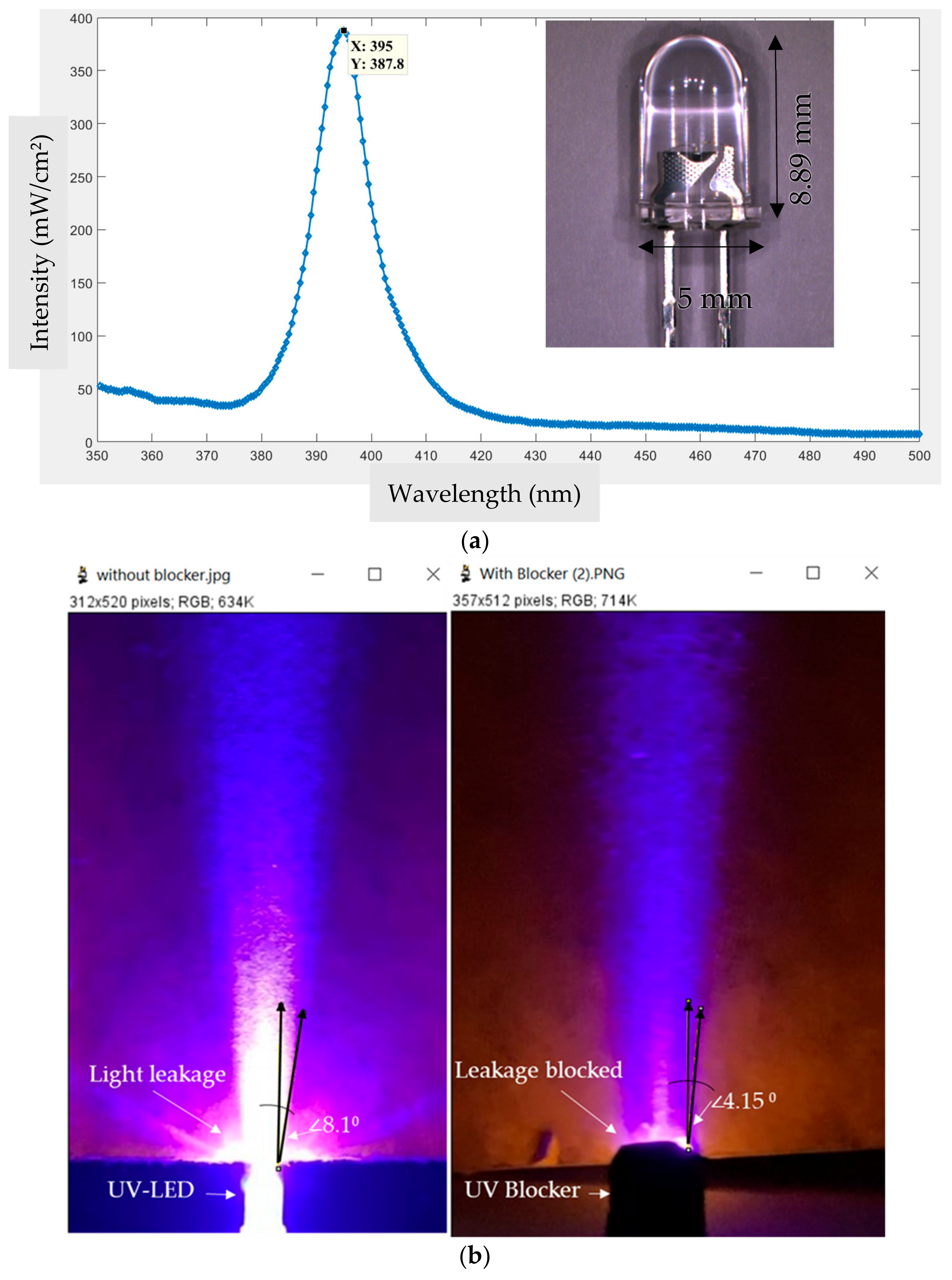
2.1. Light Source
2.2. Software
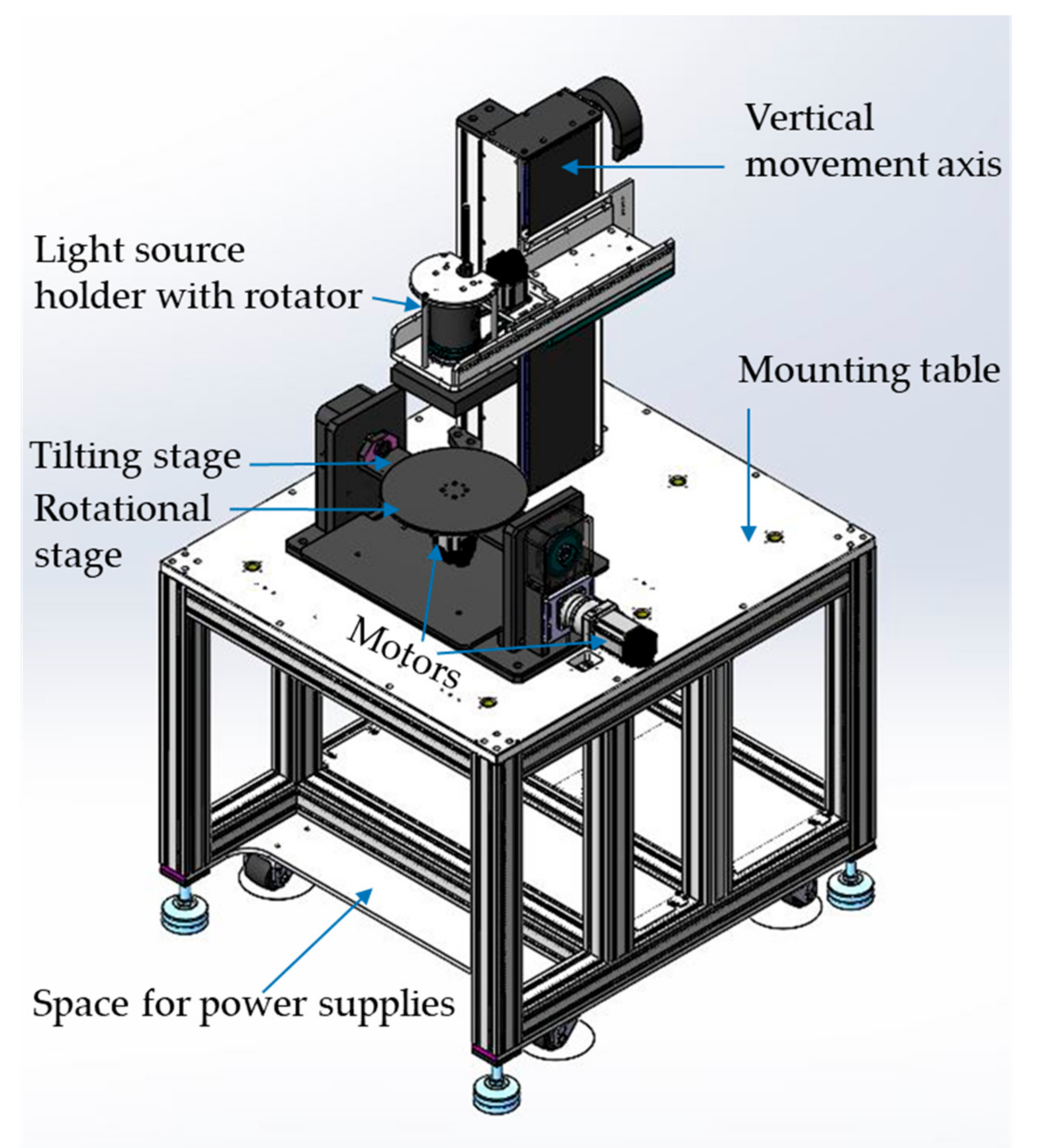
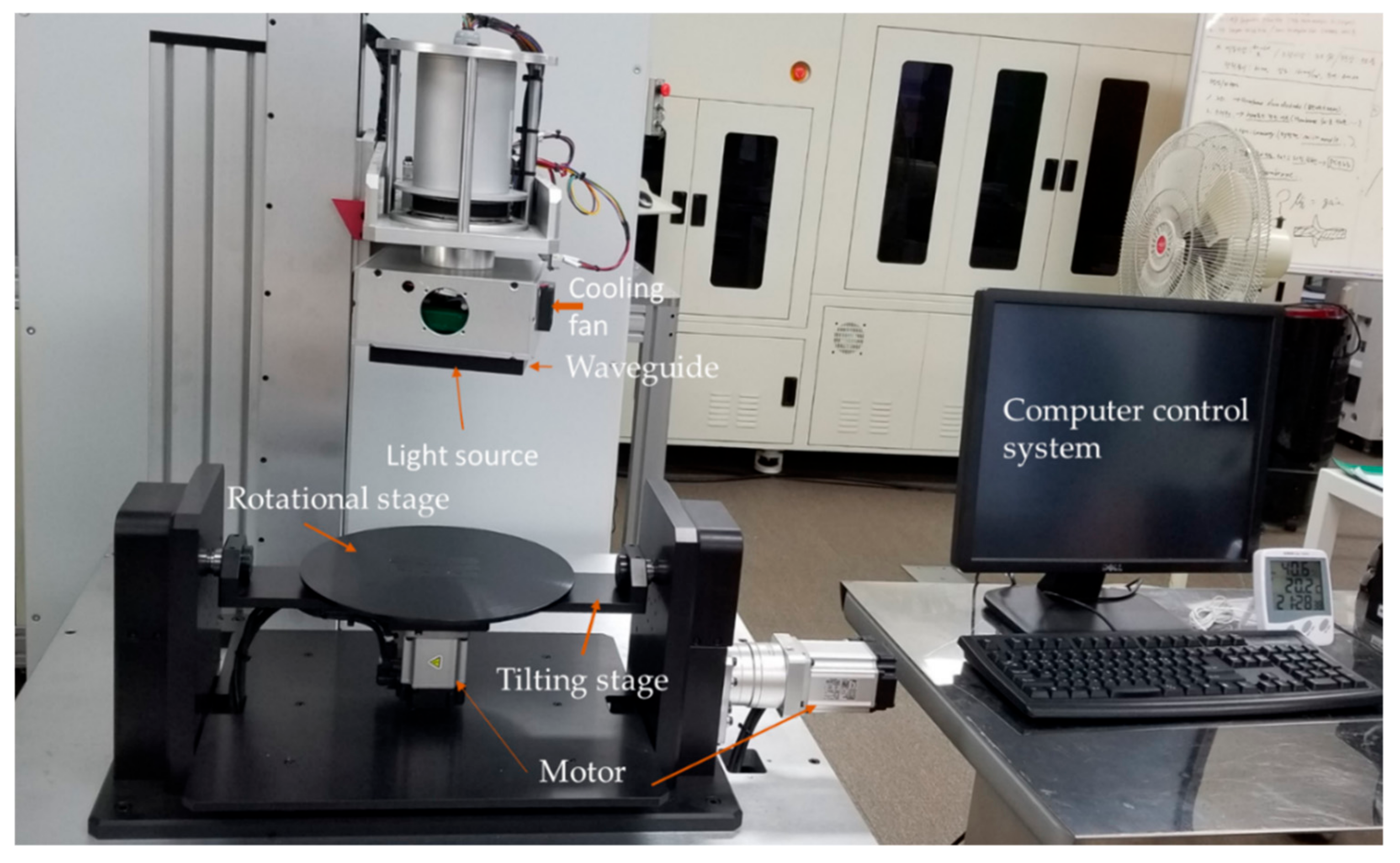
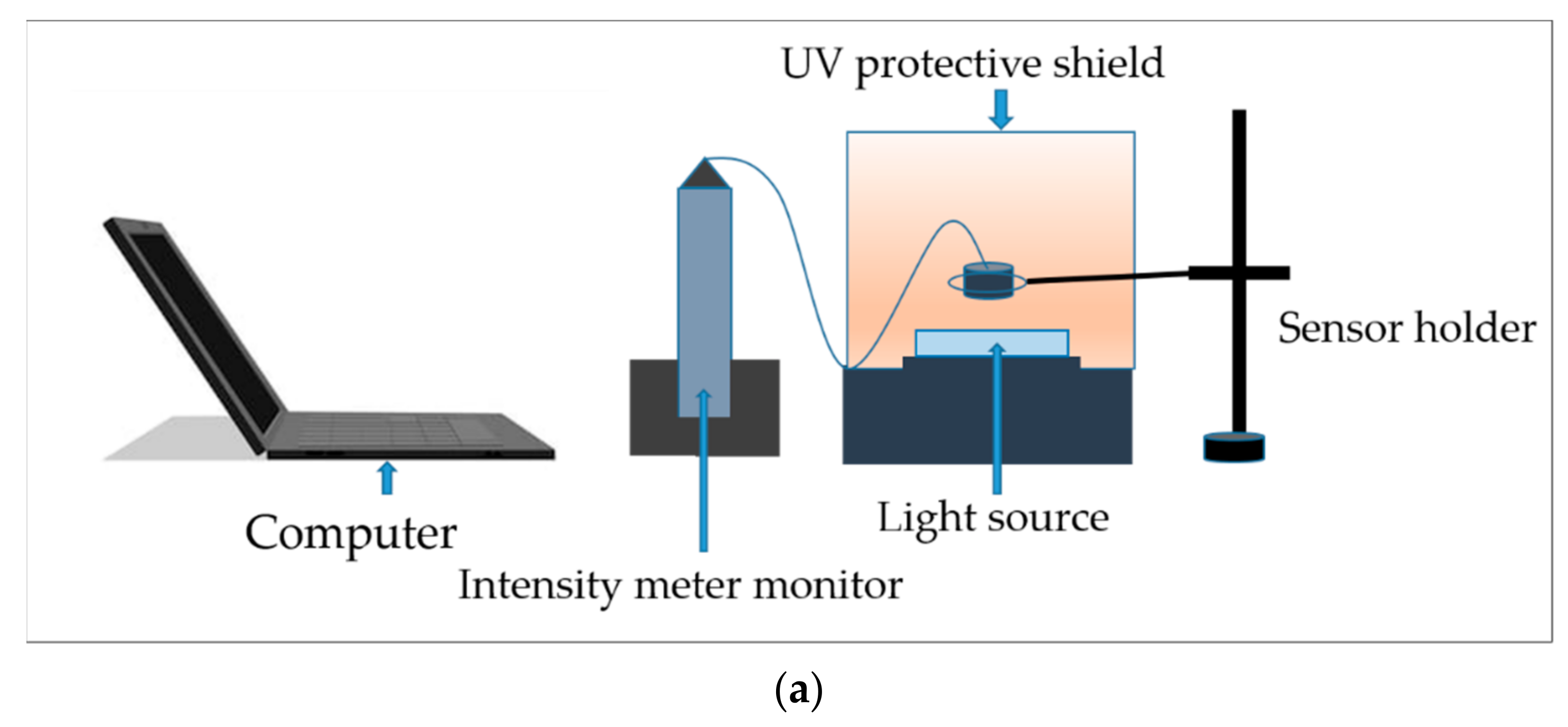
2.3. System Setup
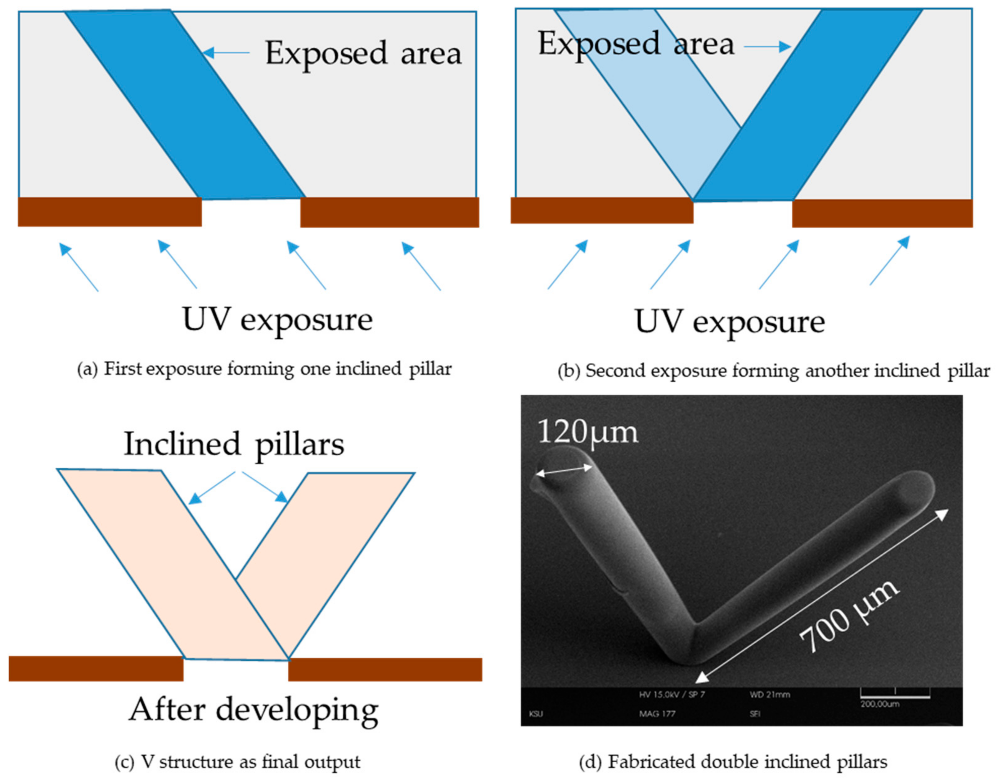
3. Fabrication Method
4. Characterization
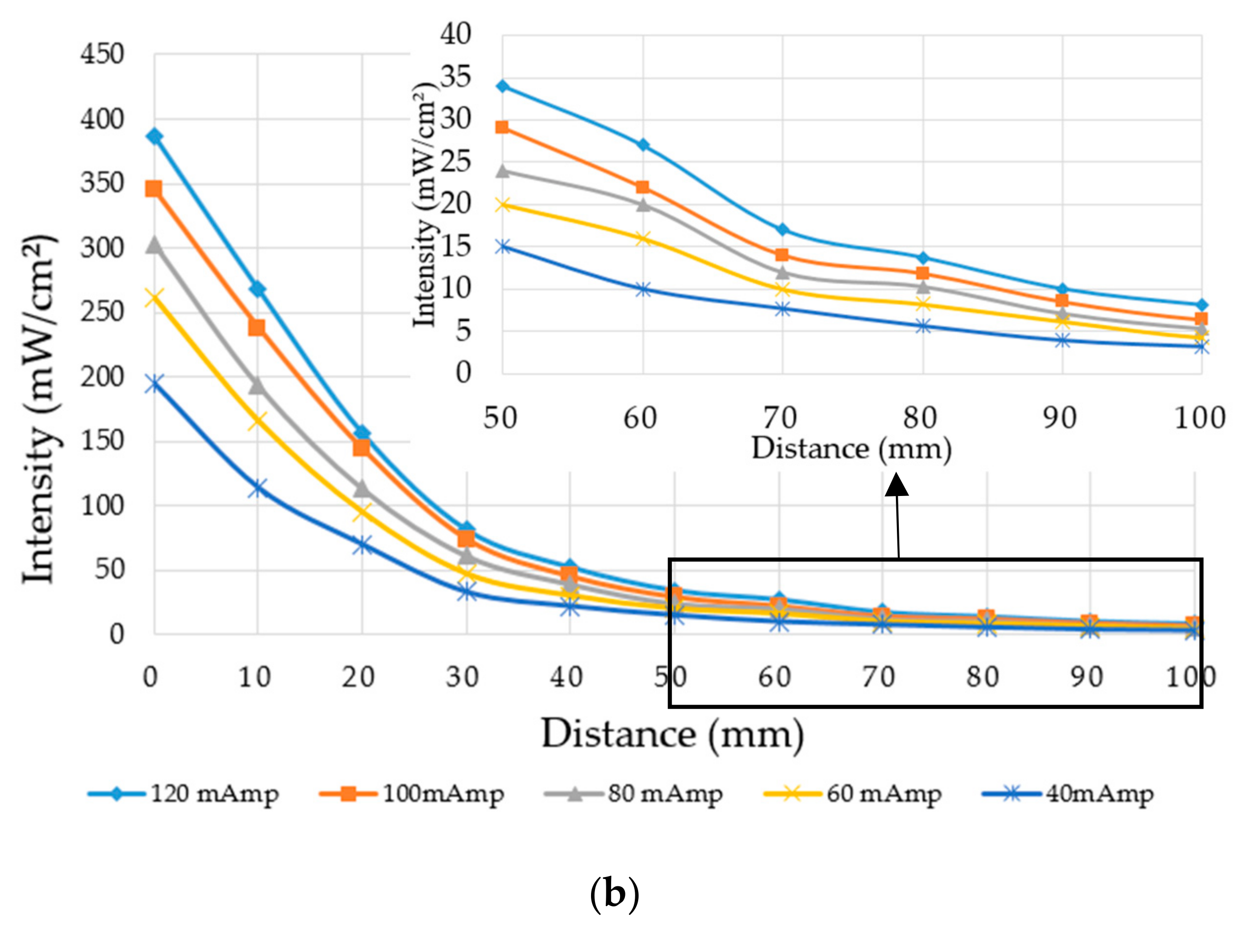
4.1. Versatility
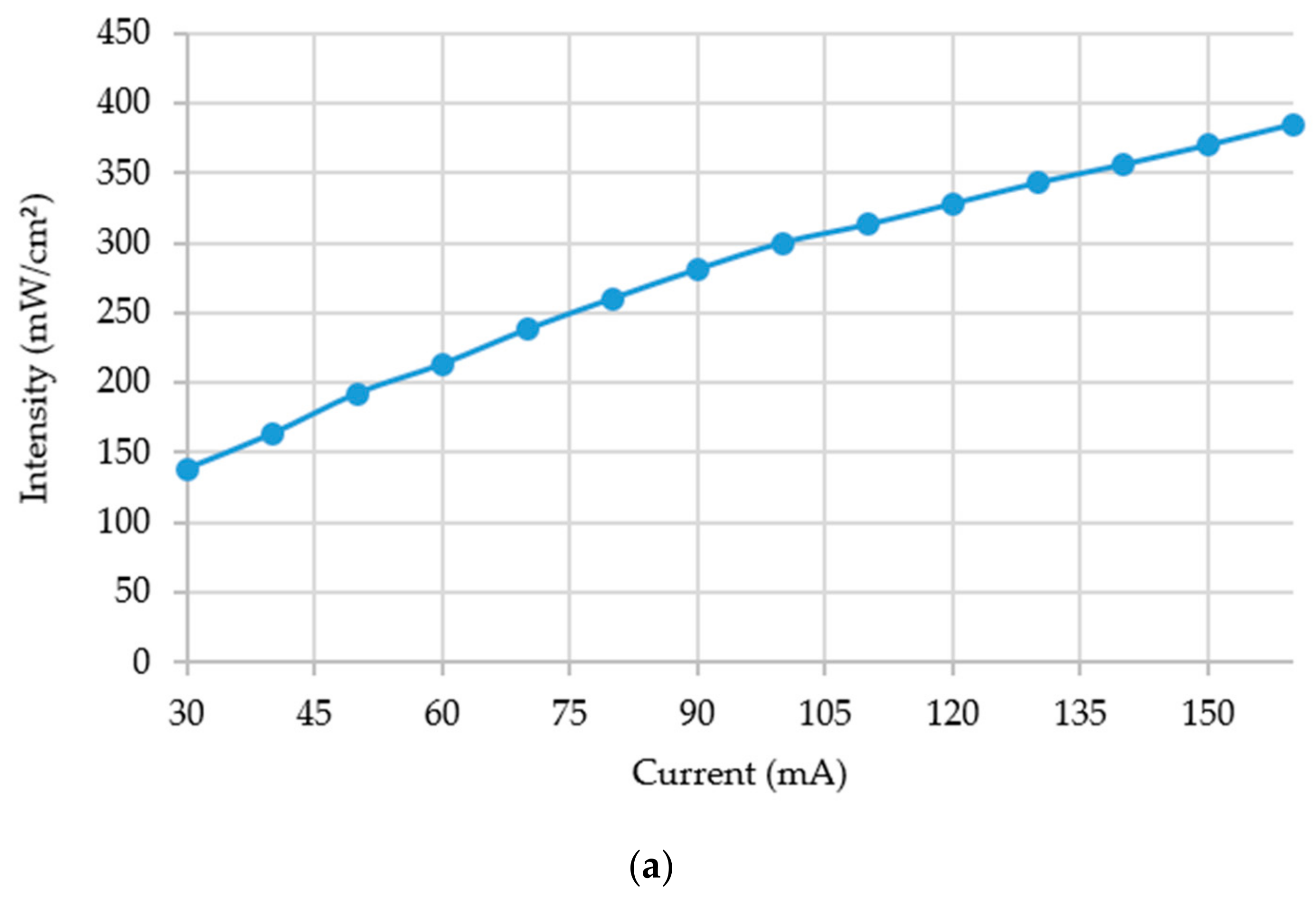
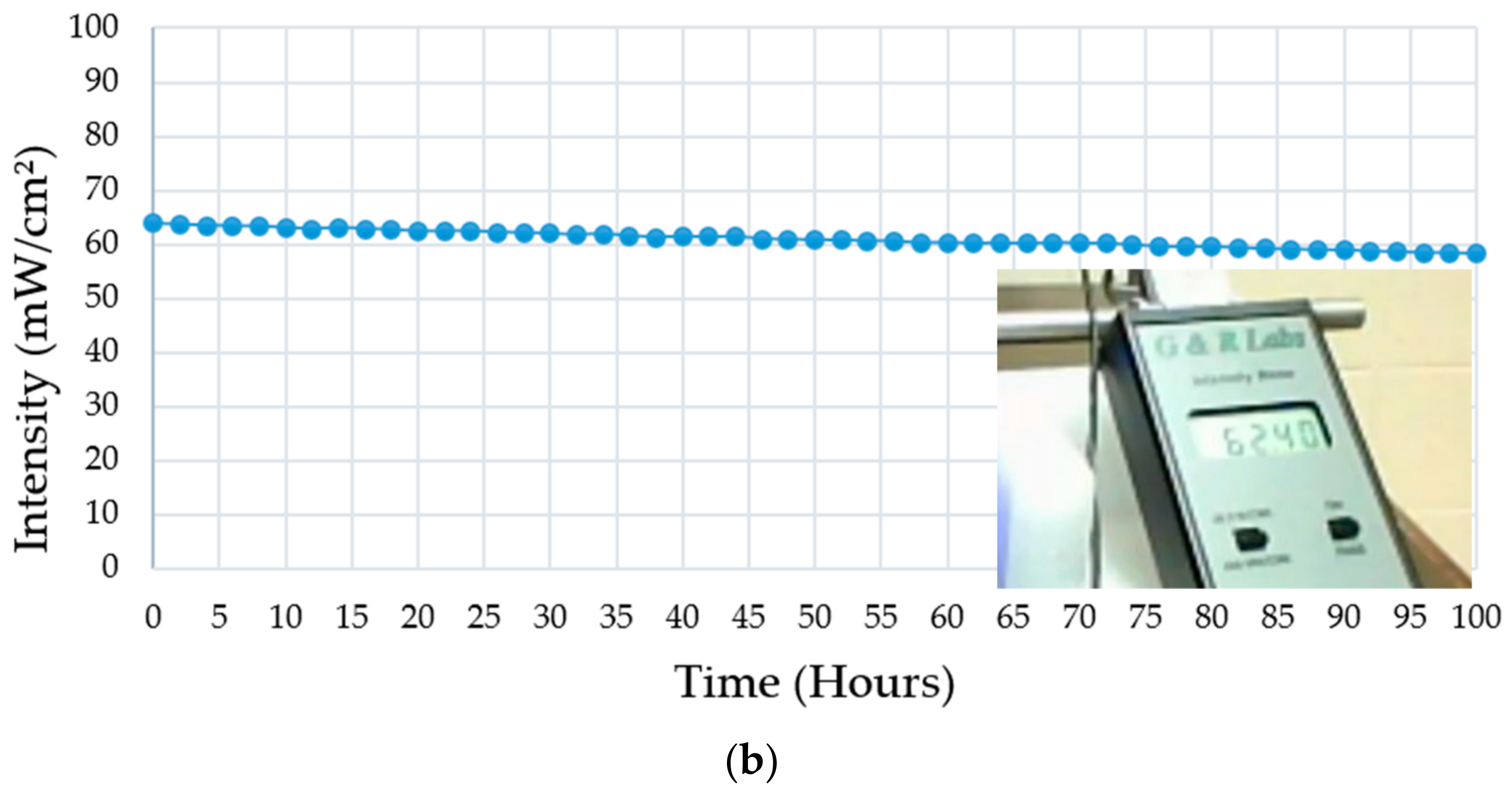
4.2. Reliability
5. Results
6. Conclusions
Author Contributions
Funding
Conflicts of Interest
References
- Alvankarian, J.; Majlis, B.Y. Exploiting the oxygen inhibitory effect on UV curing in microfabrication: A modified lithography technique. PLoS ONE 2015, 10, e0119658. [Google Scholar] [CrossRef] [PubMed]
- Ultra High Resolution Lithography. Available online: http://xraylithography.com/ (accessed on 11 December 2019).
- Song, S.H.; Lee, C.K.; Kim, T.J.; Shin, I.C.; Jun, S.C.; Jung, H.I. A rapid and simple fabrication method for 3-dimensional circular microfluidic channel using metal wire removal process. Microfluid. Nanofluid. 2010, 9, 533–540. [Google Scholar] [CrossRef]
- Proximity Mode Inclined UV Lithography. Available online: https://www.researchgate.net/publication/237539570_PROXIMITY_MODE_INCLINED_UV_LITHOGRAPHY (accessed on 11 December 2019).
- Scholten, K.; Meng, E. Electron-beam lithography for polymer bioMEMS with submicron features. Microsys. Nanoeng. 2016, 2, 16053. [Google Scholar] [CrossRef] [PubMed]
- Moon, J.H.; Yang, S. Creating three-dimensional polymeric microstructures by multi-beam interference lithography. J. Macromol. Sci. Part C: Polym. Rev. 2005, 45, 351–373. [Google Scholar] [CrossRef]
- Xie, F.; Ding, G.; Zhao, X.; Cheng, P. Design, fabrication and measurement of a novel 140 GHz folded waveguide based on SU-8 UV-LIGA technology. J. Micromech. Microeng. 2015, 25, 085010. [Google Scholar] [CrossRef]
- Zaouk, R.; Park, B.Y.; Madou, M.J. Introduction to microfabrication techniques. Methods Mol. Biol. 2006, 321, 5–15. [Google Scholar] [PubMed]
- Kim, J.J.K.; Thuwaini, H.A.; Almuslem, M. Photolithography of SU-8 microtowers for a 100-turn, 3-D toroidal microinductor. Micro Nano Sys. Lett. 2018, 6, 14. [Google Scholar] [CrossRef]
- Erickstad, M.; Gutierrez, E.; Groisman, A. A low-cost low-maintenance ultraviolet lithography light source based on light-emitting diodes. Lab Chip 2015, 15, 57–61. [Google Scholar] [CrossRef] [PubMed]
- Yapici, M.K.; Farhat, I. UV-LED exposure system for low-cost photolithography. In Proceedings of the Optical Microlithography XXVII, San Jose, CA, USA, 31 March 2014. [Google Scholar]
- Hölz, K.; Lietard, J.; Somoza, M.M. High-power 365 nm UV LED mercury arc lamp replacement for photochemistry and chemical photolithography. ACS Sustain. Chem. Eng. 2017, 5, 828–834. [Google Scholar] [CrossRef] [PubMed]
- Guijt, R.M.; Breadmore, M.C. Maskless photolithography using UV LEDs. Lab Chip 2008, 8, 1402–1404. [Google Scholar] [CrossRef] [PubMed]
- Liu, G.; Tian, Y.; Kan, Y. Fabrication of high-aspect-ratio microstructures using SU8 photoresist. Microsys. Technol. 2005, 11, 343–346. [Google Scholar] [CrossRef]
- del Campo, A.; Greiner, C. SU-8: A photoresist for high-aspect-ratio and 3D submicron lithography. J. Micromech. Microeng. 2007, 17, R81. [Google Scholar] [CrossRef]
- Sato, H.; Houshi, Y.; Shoji, S. Three-dimensional micro-structures consisting of high aspect ratio inclined micro-pillars fabricated by simple photolithography. Microsys. Technol. 2004, 10, 440–443. [Google Scholar] [CrossRef]
- Yoon, Y.K.; Park, J.H.; Allen, M.G. Multidirectional UV lithography for complex 3-D MEMS structures. J. Microelectromechanical Syst. 2006, 15, 1121–1130. [Google Scholar] [CrossRef]
- Kim, J.; Allen, M.G.; Yoon, Y.K. Automated dynamic mode multidirectional UV lithography for complex 3-D microstructures. In Proceedings of the IEEE 21st International Conference on Micro Electro Mechanical Systems (MEMS), Wuhan, China, 13–17 January 2008. [Google Scholar]
- Kim, J.; Cheng, X.; Senior, D.E.; Allen, M.G.; Yoon, Y.K. Three dimensional nanoscale fabrication and modeling of dynamic mode multidirectional UV lithography. In Proceedings of the 16th International Solid-State Sensors, Actuators and Microsystems Conference, Beijing, China, 5–9 June 2011. [Google Scholar]
- Kim, J.; Yoon, Y.K.; Allen, M.G. Computer numerical control (CNC) lithography: Light-motion synchronized UV-LED lithography for 3D microfabrication. J. Micromech. Microeng. 2016, 26, 035003. [Google Scholar] [CrossRef]


© 2020 by the authors. Licensee MDPI, Basel, Switzerland. This article is an open access article distributed under the terms and conditions of the Creative Commons Attribution (CC BY) license (http://creativecommons.org/licenses/by/4.0/).
Share and Cite
Shiba, S.F.; Jeon, H.; Kim, J.-S.; Kim, J.-E.; Kim, J. 3D Microlithography Using an Integrated System of 5-mm UV-LEDs with a Tilt-Rotational Sample Holder. Micromachines 2020, 11, 157. https://doi.org/10.3390/mi11020157
Shiba SF, Jeon H, Kim J-S, Kim J-E, Kim J. 3D Microlithography Using an Integrated System of 5-mm UV-LEDs with a Tilt-Rotational Sample Holder. Micromachines. 2020; 11(2):157. https://doi.org/10.3390/mi11020157
Chicago/Turabian StyleShiba, Sabera Fahmida, Hyeongmin Jeon, Jong-Soo Kim, Jong-Eun Kim, and Jungkwun Kim. 2020. "3D Microlithography Using an Integrated System of 5-mm UV-LEDs with a Tilt-Rotational Sample Holder" Micromachines 11, no. 2: 157. https://doi.org/10.3390/mi11020157
APA StyleShiba, S. F., Jeon, H., Kim, J.-S., Kim, J.-E., & Kim, J. (2020). 3D Microlithography Using an Integrated System of 5-mm UV-LEDs with a Tilt-Rotational Sample Holder. Micromachines, 11(2), 157. https://doi.org/10.3390/mi11020157