Pore Structures for High-Throughput Nanopore Devices


Abstract

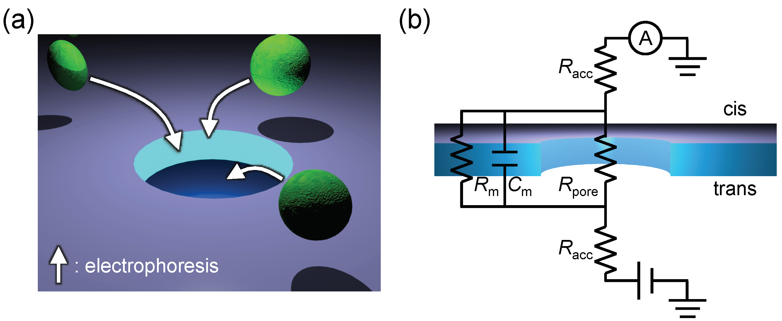
1. Introduction
2. Methods
3. Results and Discussion
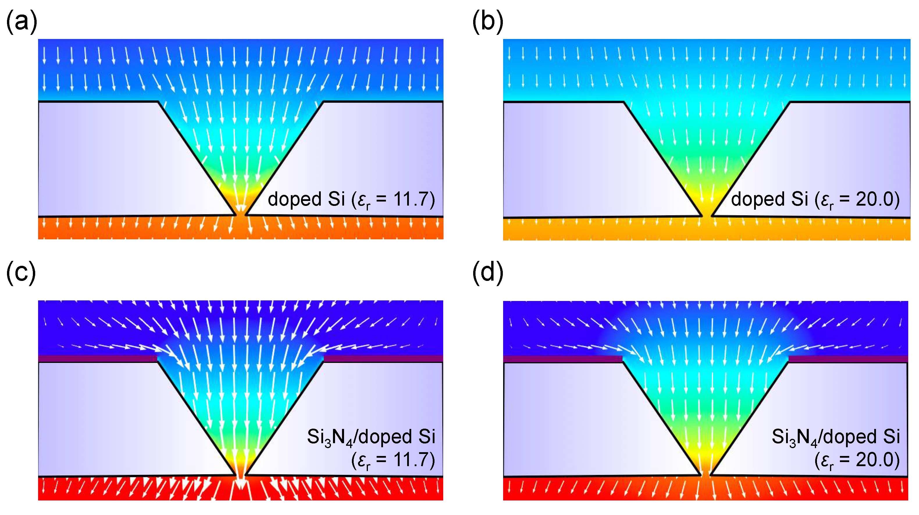
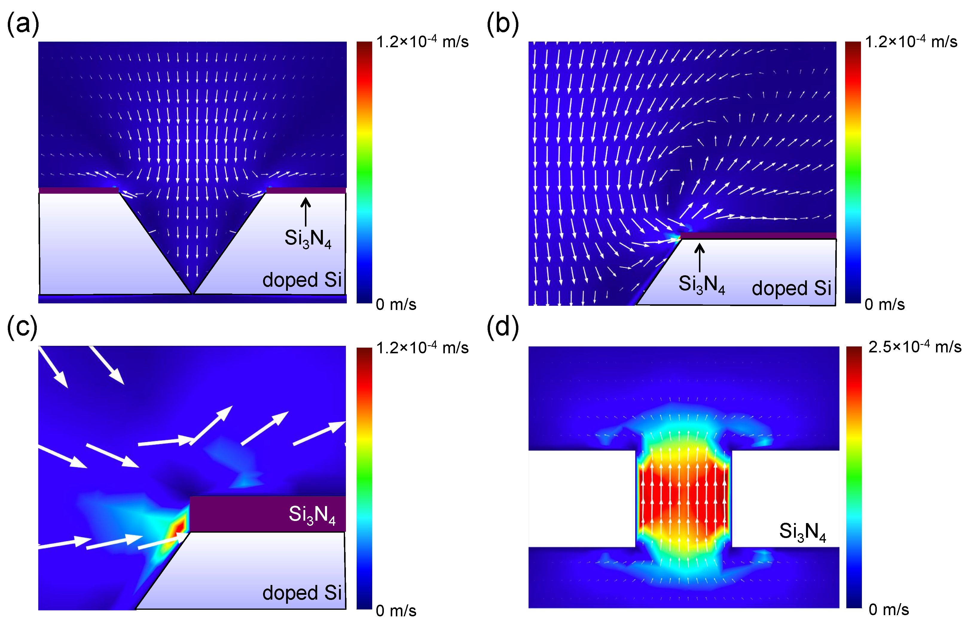
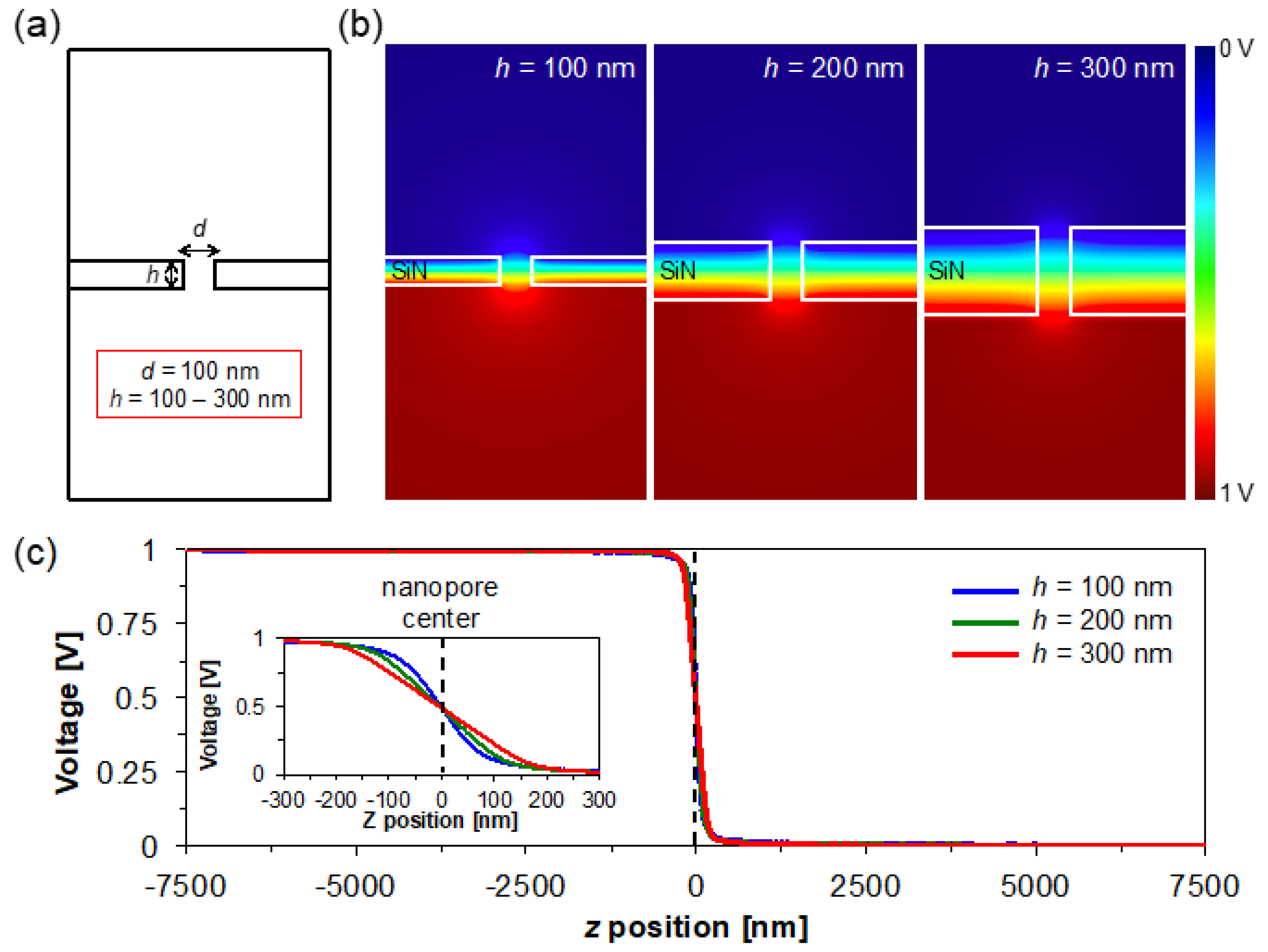
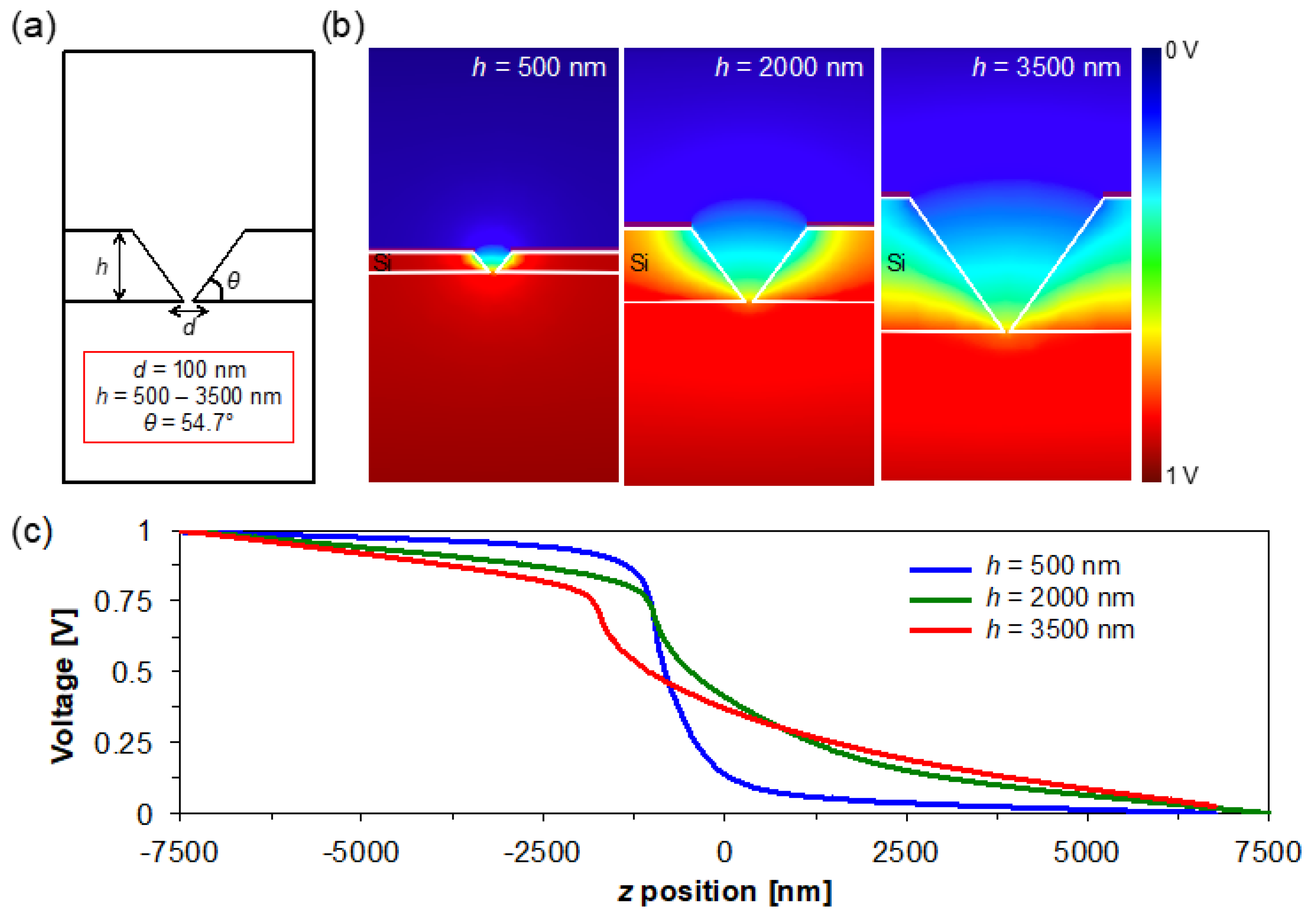
3.1. Electric Field Gradients in Nanopore Devices
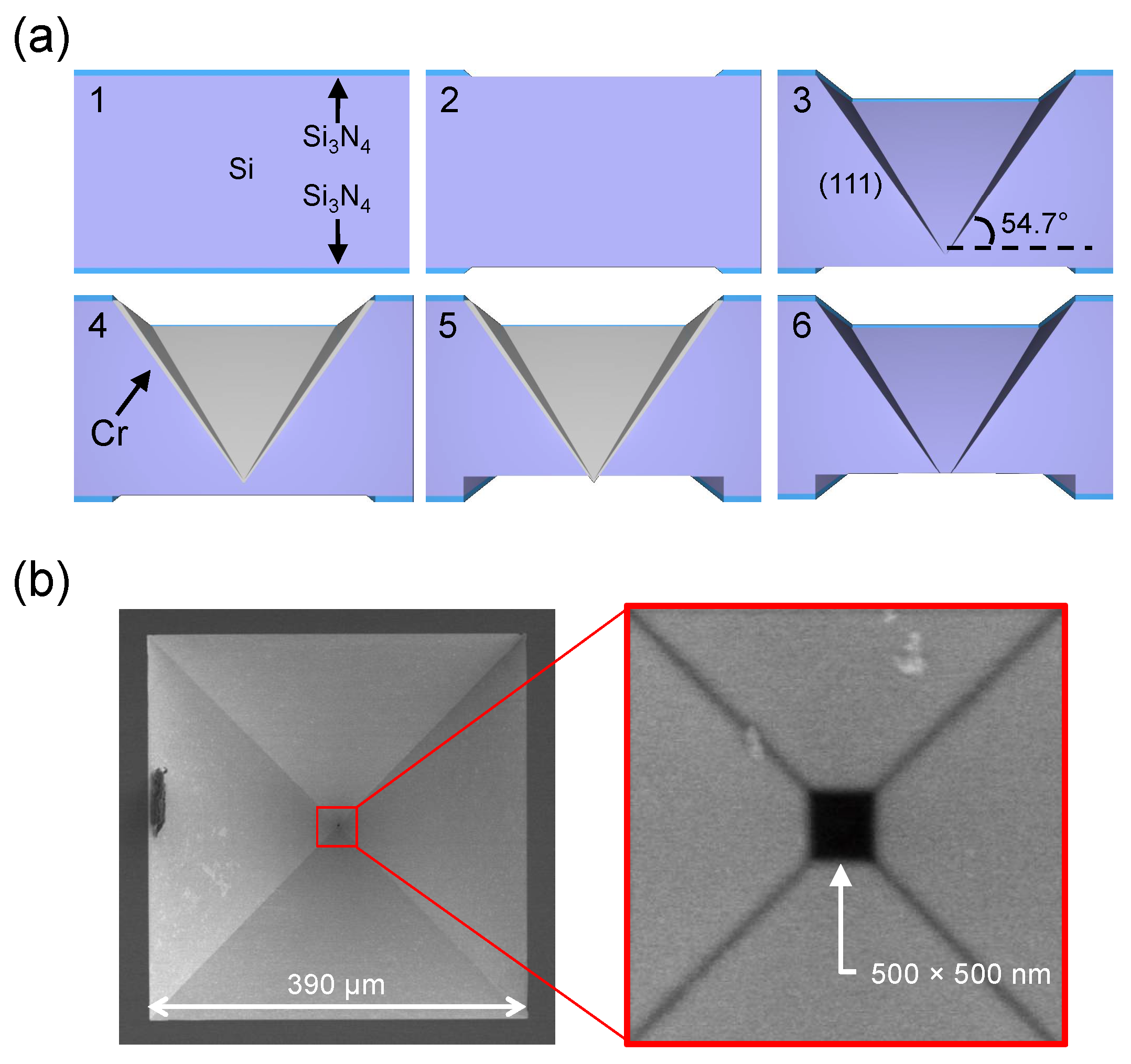
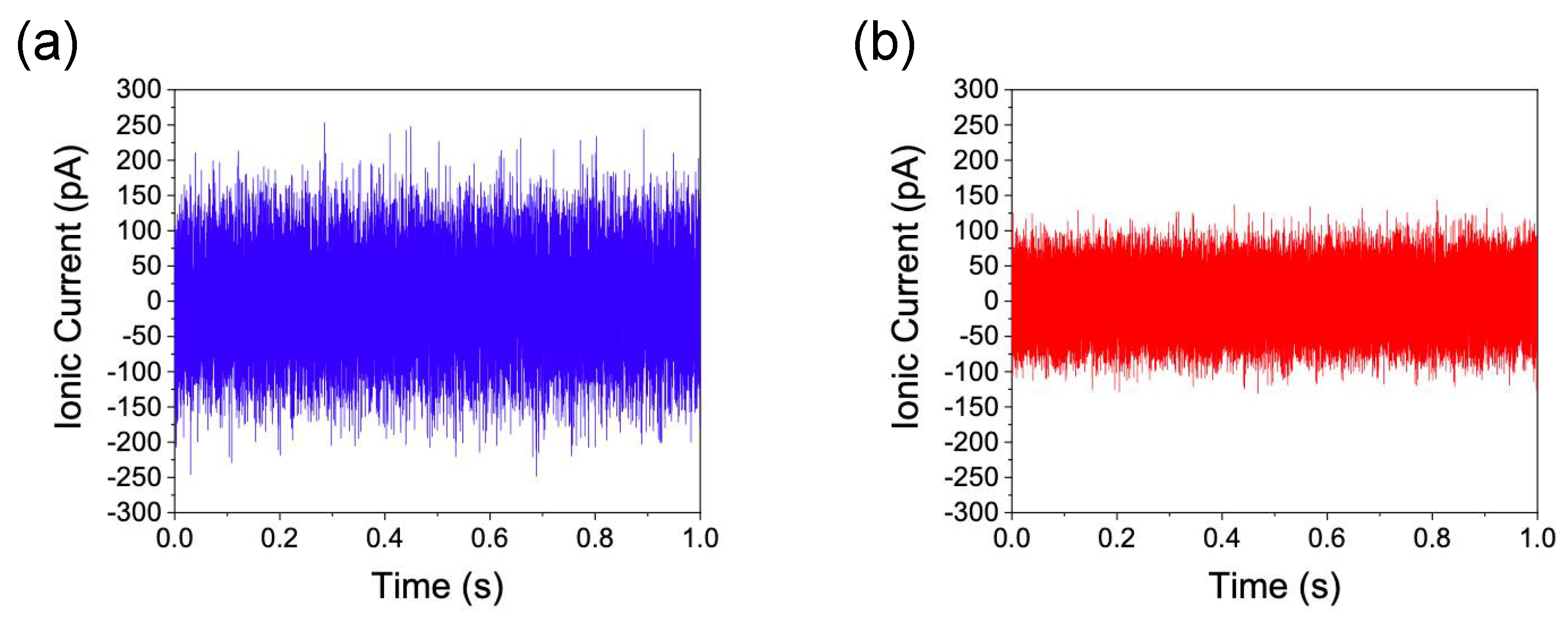
3.2. Fabrications and Ionic Current Noise Level of the IP-Shaped Nanopore Devices
4. Conclusions
Supplementary Materials
Author Contributions
Funding
Acknowledgments
Conflicts of Interest
Appendix A

Appendix B

References
- Cheng, M.H.; Bahar, I. Monoamine Transporters: Structure, Intrinsic Dynamics and Allosteric Regulation. Nat. Struct. Mol. Biol. 2019, 26, 545–556. [Google Scholar] [CrossRef]
- Venkatesan, B.M.; Bashir, R. Nanopore Sensors for Nucleic Acid Analysis. Nat. Nanotechnol. 2011, 6, 615–624. [Google Scholar] [CrossRef]
- Dekker, C. Solid-State Nanopores. Nat. Nanotechnol. 2007, 2, 209–215. [Google Scholar] [CrossRef]
- Tu, B.; Bai, S.; Lu, B.; Fang, Q. Conic shapes have higher sensitivity than cylindrical ones in nanopore DNA sequencing. Sci. Rep. 2018, 8, 9097. [Google Scholar] [CrossRef]
- Di Ventra, M.; Taniguchi, M. Decoding DNA, RNA and Peptides with Quantum Tunnelling. Nat. Nanotechnol. 2016, 11, 117–126. [Google Scholar] [CrossRef]
- Arima, A.; Tsutsui, M.; Harlisa, I.H.; Yoshida, T.; Tanaka, M.; Yokota, K.; Tonomura, W.; Taniguchi, M.; Okochi, M.; Washio, T.; et al. Selective Detections of Single-Viruses Using Solid-State Nanopores. Sci. Rep. 2018, 8, 16305. [Google Scholar] [CrossRef]
- Ryuzaki, S.; Tsutsui, M.; He, Y.; Yokota, K.; Arima, A.; Morikawa, T.; Taniguchi, M.; Kawai, T. Rapid Structural Analysis of Nanomaterials in Aqueous Solutions. Nanotechnology 2017, 28, 155501. [Google Scholar] [CrossRef]
- Tsutsui, M.; Hongo, S.; He, Y.; Taniguchi, M.; Gemma, N.; Kawai, T. Single-Nanoparticle Detection Using a Low-Aspect-Ratio Pore. ACS Nano 2012, 6, 3499–3505. [Google Scholar] [CrossRef]
- Bell, N.A.W.; Muthukumar, M.; Keyser, U.F. Translocation Frequency of Double-Stranded DNA through a Solid-State Nanopore. Phys. Rev. E 2016, 93, 1–10. [Google Scholar] [CrossRef]
- He, Y.; Gillespie, D.; Boda, D.; Vlassiouk, I.; Eisenberg, R.S.; Siwy, Z.S. Tuning Transport Properties of Nanofluidic Devices with Local Charge Inversion. J. Am. Chem. Soc. 2009, 131, 5194–5202. [Google Scholar] [CrossRef]
- Huang, S.; Romero-Ruiz, M.; Castell, O.K.; Bayley, H.; Wallace, M.I. High-Throughput Optical Sensing of Nucleic Acids in a Nanopore Array. Nat. Nanotechnol. 2015, 10, 986–991. [Google Scholar] [CrossRef] [PubMed]
- McNally, B.; Singer, A.; Yu, Z.; Sun, Y.; Weng, Z.; Meller, A. Optical Recognition of Converted DNA Nucleotides for Single-Molecule DNA Sequencing Using Nanopore Arrays. Nano Lett. 2010, 10, 2237–2244. [Google Scholar] [CrossRef] [PubMed]
- Bell, N.A.W.; Thacker, V.V.; Hernández-Ainsa, S.; Fuentes-Perez, M.E.; Moreno-Herrero, F.; Liedl, T.; Keyser, U.F. Multiplexed Ionic Current Sensing with Glass Nanopores. Lab Chip 2013, 13, 1859–1862. [Google Scholar] [CrossRef] [PubMed]
- Vogel, R.; Willmott, G.; Kozak, D.; Roberts, G.S.; Anderson, W.; Groenewegen, L.; Glossop, B.; Barnett, A.; Turner, A.; Trau, M. Quantitative Sizing of Nano/Microparticles with a Tunable Elastomeric Pore Sensor. Anal. Chem. 2011, 83, 3499–3506. [Google Scholar] [CrossRef] [PubMed]
- Liang, S.; Xiang, F.; Tang, Z.; Nouri, R.; He, X.; Dong, M.; Guan, W. Noise in Nanopore Sensors: Sources, Models, Reduction, and Benchmarking. Nanotechnol. Precis. Eng. 2020, 3, 9–17. [Google Scholar] [CrossRef]
- He, Y.; Tsutsui, M.; Fan, C.; Taniguchi, M.; Kawai, T. Controlling DNA Translocation through Gate Modulation of Nanopore Wall Surface Charges. ACS Nano 2011, 5, 5509–5518. [Google Scholar] [CrossRef]
- He, Y.; Tsutsui, M.; Fan, C.; Taniguchi, M.; Kawai, T. Gate Manipulation of DNA Capture into Nanopores. ACS Nano 2011, 5, 8391–8397. [Google Scholar] [CrossRef]
- Golla, E. Use of Silicon as a Semiconductor. In Crystal Growth and Evaluation of Silicon for VLSI and ULSI; CRC Press: Boca Raton, FL, USA, 2014; p. 7. [Google Scholar]
- Ristic, S.; Prijic, A.; Prijic, Z. Dependence of Static Dielectric Constant of Silicon on Resistivity at Room Temperature. Serb. J. Electr. Eng. 2004, 1, 237–247. [Google Scholar] [CrossRef]
- Dow, H.S.; Kim, W.S.; Lee, J.W. Thermal and Electrical Properties of Silicon Nitride Substrates. AIP Adv. 2017, 7, 095022. [Google Scholar] [CrossRef]
- Chou, C.Y.; Lin, C.H.; Chen, W.H.; Li, B.J.; Liu, C.Y. High-Dielectric-Constant Silicon Nitride Thin Films Fabricated by Radio Frequency Sputtering in Ar and Ar/N2 Gas Mixture. Thin Solid Films 2020, 709, 138198. [Google Scholar] [CrossRef]
- Masetti, G.; Severi, M.; Solmi, S. Modeling of Carrier Mobility Against Carrier Concentration in Arsenic-, Phosphorus-, and Boron-Doped Silicon. IEEE Trans. Electron. Dev. 1983, 30, 764–765. [Google Scholar] [CrossRef]
- Zeng, S.; Wen, C.; Solomon, P.; Zhang, S.L.; Zhang, Z. Rectification of Protein Translocation in Truncated Pyramidal Nanopores. Nat. Nanotechnol. 2019, 14, 1056–1062. [Google Scholar] [CrossRef] [PubMed]
- Tsutsui, M.; Maeda, Y.; He, Y.; Hongo, S.; Ryuzaki, S.; Kawano, S.; Kawai, T.; Taniguchi, M. Trapping and Identifying Single-Nanoparticles Using a Low-Aspect-Ratio Nanopore. Appl. Phys. Lett. 2013, 103, 013108. [Google Scholar] [CrossRef]
- Laohakunakorn, N.; Thacker, V.; Muthukumar, M.; Keyser, U. Electroosmotic Flow Reversal outside Glass Nanopores. Nano Lett. 2015, 15, 695–702. [Google Scholar] [CrossRef]
- Arjmandi, N.; Van Roy, W.; Lagae, L.; Borghs, G. Measuring the Electric Charge and Zeta Potential of Nanometer-Sized Objects Using Pyramidal-Shaped Nanopores. Anal. Chem. 2012, 84, 8490–8496. [Google Scholar] [CrossRef]
- Langecker, M.; Pedone, D.; Simmel, F.C.; Rant, U. Electrophoretic Time-of-Flight Measurements of Single DNA Molecules with Two Stacked Nanopores. Nano Lett. 2011, 11, 5002–5007. [Google Scholar] [CrossRef]
- Matsuda, R.; Ryuzaki, S.; Okamoto, K.; Arima, Y.; Tsutsui, M.; Taniguchi, M.; Tamada, K. Finite-Difference Time-Domain Simulations of Inverted Cone-Shaped Plasmonic Nanopore Structures. J. Appl. Phys. 2020, 127, 243109. [Google Scholar] [CrossRef]
- Davenport, M.; Healy, K.; Pevarnik, M.; Teslich, N.; Cabrini, S.; Morrison, A.P.; Siwy, Z.S.; Létant, S.E. The Role of Pore Geometry in Single Nanoparticle Detection. ACS Nano 2012, 6, 8366–8380. [Google Scholar] [CrossRef]


© 2020 by the authors. Licensee MDPI, Basel, Switzerland. This article is an open access article distributed under the terms and conditions of the Creative Commons Attribution (CC BY) license (http://creativecommons.org/licenses/by/4.0/).
Share and Cite
Ryuzaki, S.; Matsuda, R.; Taniguchi, M. Pore Structures for High-Throughput Nanopore Devices. Micromachines 2020, 11, 893. https://doi.org/10.3390/mi11100893
Ryuzaki S, Matsuda R, Taniguchi M. Pore Structures for High-Throughput Nanopore Devices. Micromachines. 2020; 11(10):893. https://doi.org/10.3390/mi11100893
Chicago/Turabian StyleRyuzaki, Sou, Rintaro Matsuda, and Masateru Taniguchi. 2020. "Pore Structures for High-Throughput Nanopore Devices" Micromachines 11, no. 10: 893. https://doi.org/10.3390/mi11100893
APA StyleRyuzaki, S., Matsuda, R., & Taniguchi, M. (2020). Pore Structures for High-Throughput Nanopore Devices. Micromachines, 11(10), 893. https://doi.org/10.3390/mi11100893