Design and Performance of a J Band MEMS Switch


Abstract
:1. Introduction
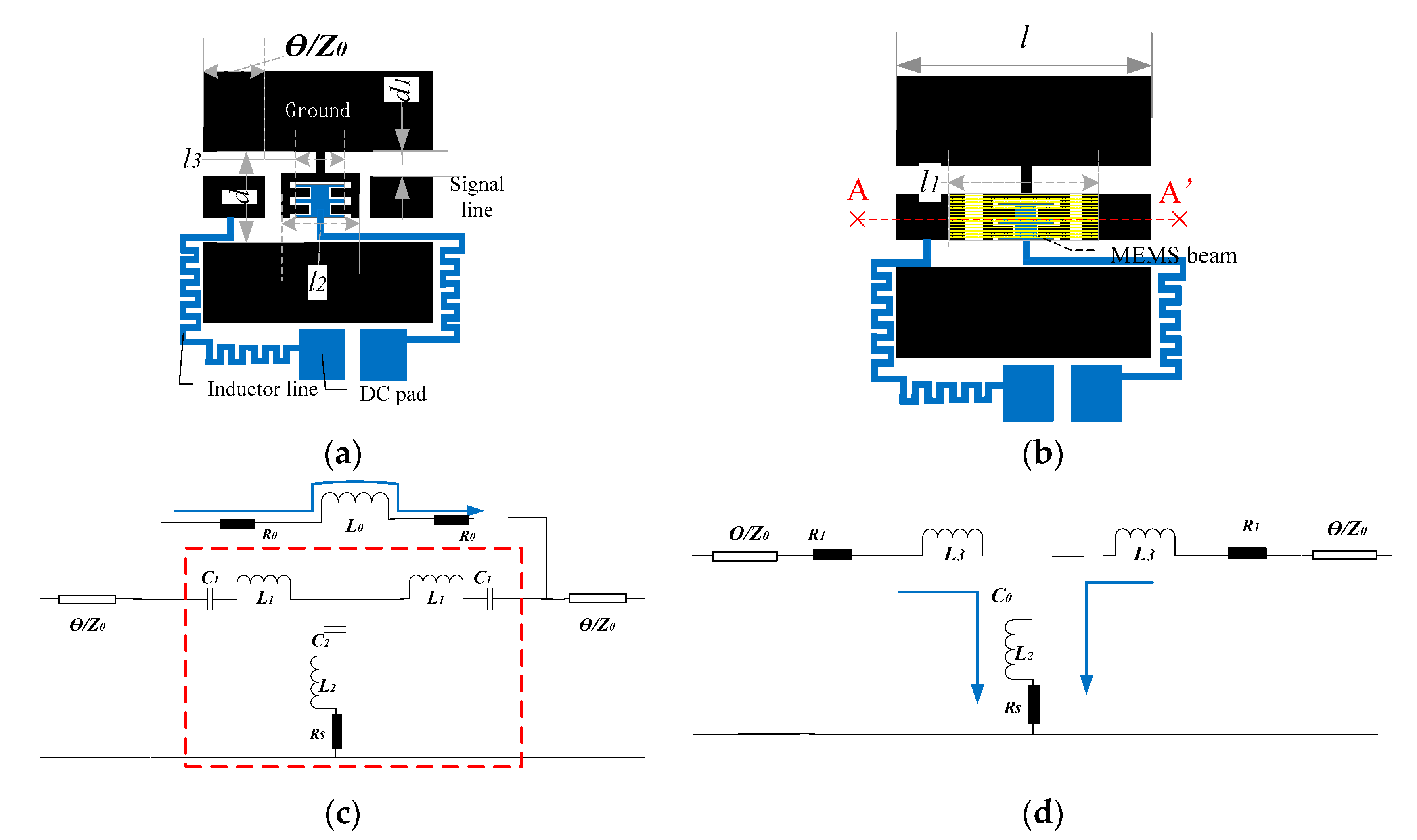
2. Design
2.1. Radio Frequency Analysis
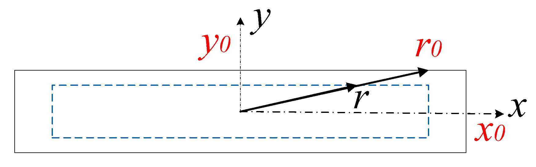
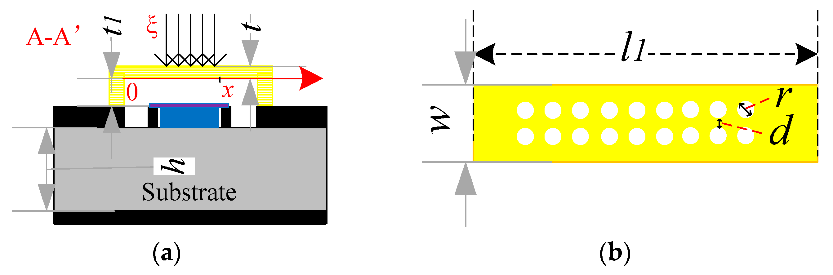
2.2. Analysis of Mechanical Properties
- (a)
- The elastic coefficient k1 is due to the stiffness of the bridge, which accounts for the material characteristics such as Young’s modulus [10], E (Pa), and the moment of inertia, I (m4) = l1t2/12, t is the thickness of switch beam.The deflection (y1) found by evaluating the integral is,Elastic coefficient (k1) caused by Stiffness of Beams is,
- (b)
- The elastic coefficient k2 is due to the biaxial residual stress, S’(Pa) = σ(1 − ν)l1t, where ν is the Poisson’s ratio [8].The deflection (y2) found by evaluating the integral is,Elastic coefficients induced by biaxial residual stresses is,
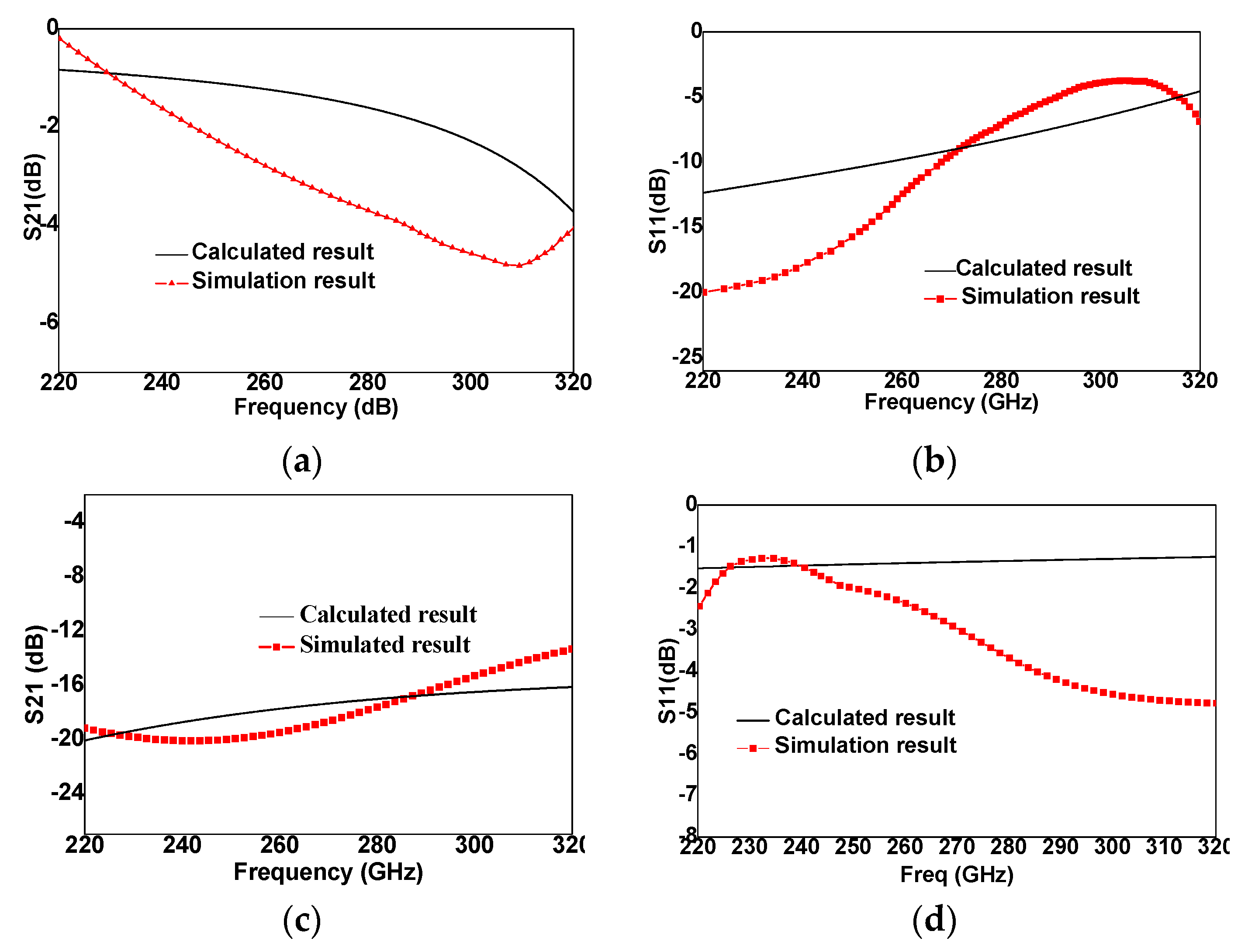
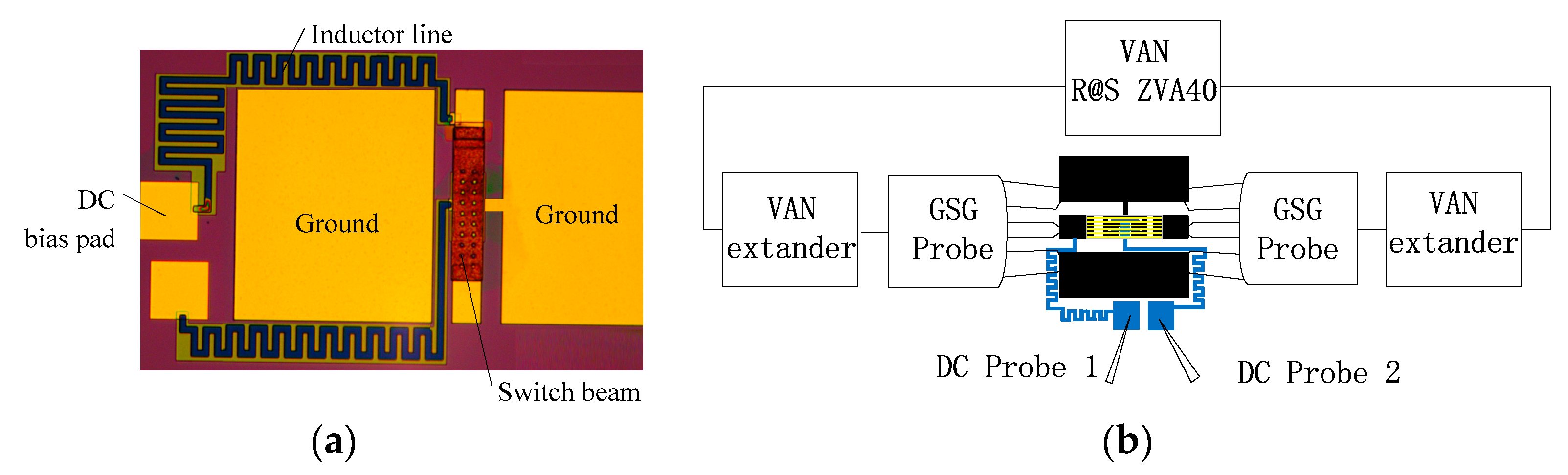
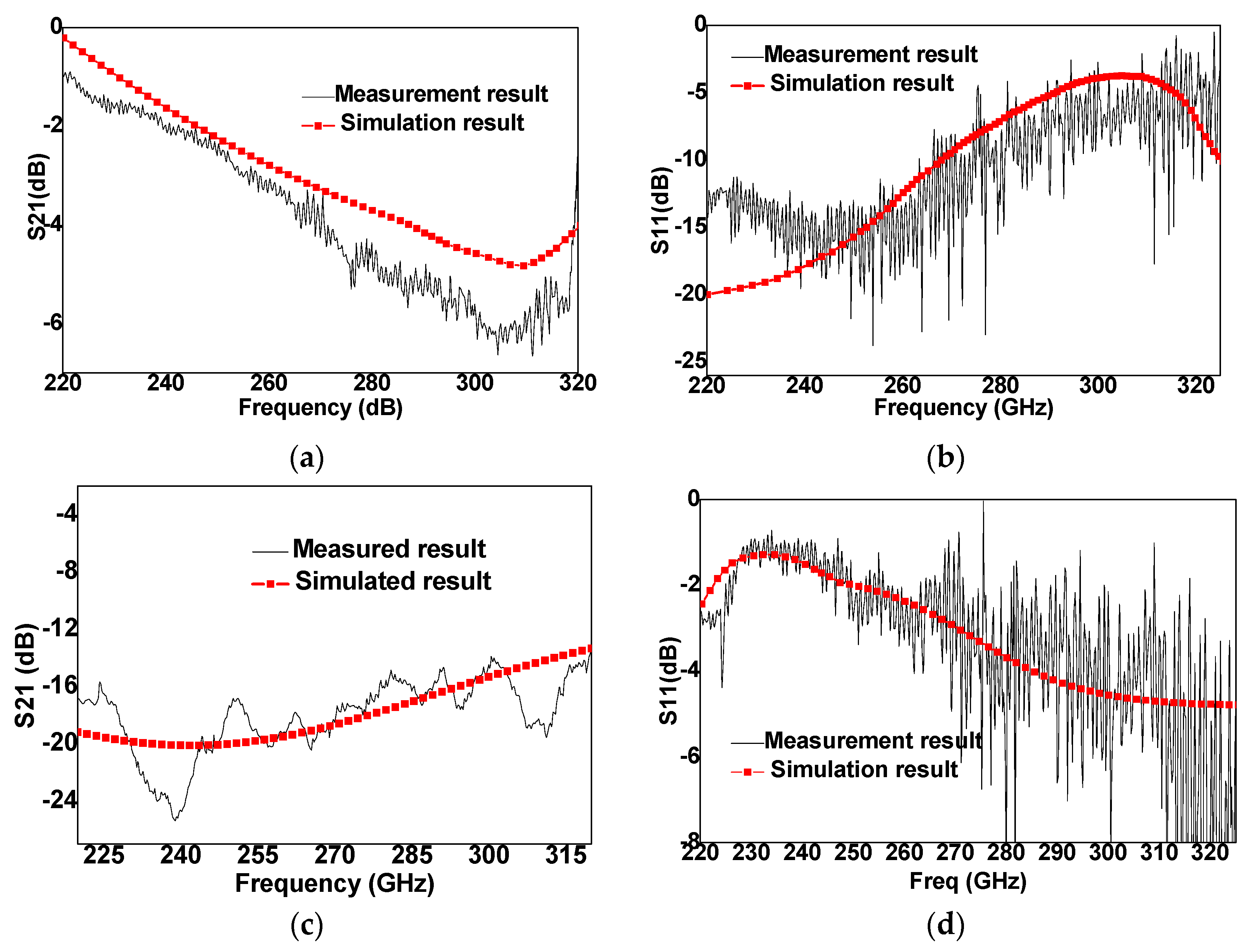
3. Results
4. Discussion
5. Conclusions
Author Contributions
Funding
Conflicts of Interest
References
- Du, Y.J.; Su, W.; Tolunay, S.; Zhang, L.; Kaynak, M.; Scholz, R.; Xiong, Y.Z. 220GHz wide-band MEMS switch in standard BiCMOS technology. In Proceedings of the 2015 IEEE Asian Solid-State Circuits Conference (A-SSCC), Xiamen, China, 9–11 November 2015; pp. 1–4. [Google Scholar]
- Wipf, S.T.; Göritz, A.; Wietstruck, M.; Wipf, C.; Tillack, B.; Kaynak, M. D-Band RF-MEMS SPDT Switch in a 0.13 μm SiGe BiCMOS Technology. IEEE Microw. Wirel. Compon. Lett. 2016, 26, 1002–1004. [Google Scholar] [CrossRef]
- Feng, Y.; Barker, N.S. High performance 500–750 GHz RF MEMS switch. In Proceedings of the 2017 IEEE MTT-S International Microwave Symposium (IMS), Honololu, HI, USA, 4–9 June 2017; pp. 1095–1097. [Google Scholar]
- Sudhanshu, S.; Vinoy, K.J.; Ananthasuresh, G.K. Surface-Micromachined Capacitive RF Switches with Low Actuation Voltage and Steady Contact. J. Microelectromech. Syst. 2017, 26, 643–652. [Google Scholar]
- Persano, A.; Quaranta, F.; Capoccia, G.; Proietti, E.; Lucibello, A.; Marcelli, R.; Bagolini, A.; Iannacci, J.; Taurino, A.; Siciliano, P. Influence of design and fabrication on RF performance of capacitive RF MEMS switches. Microsyst. Technol. 2016, 22, 1741–1746. [Google Scholar] [CrossRef]
- Laemmle, D.; Schlaak, H.F.; Weickhmann, C.; Jakoby, R. Proof of concept for a WR-2.2 MEMS waveguide switch. In Proceedings of the 2016 41st International Conference on Infrared, Millimeter, and Terahertz waves (IRMMW-THz), Copenhagen, Denmark, 25–30 September 2016; pp. 1–2. [Google Scholar]
- Shah, U.; Reck, T.; Frid, H.; Jung-Kubiak, C.; Chattopadhyay, G.; Mehdi, I.; Oberhammer, J. A 500–750 GHz RF MEMS Waveguide Switch. IEEE Trans. Terahertz Sci. Technol. 2017, 7, 326–334. [Google Scholar] [CrossRef]
- Rebeiz, G.M. RF MEMS: Theory, Design, and Technology; John Wiley & Sons: Hoboken, NJ, USA, 2004. [Google Scholar]
- Zhang, N.; Wang, C.; Lang, L.; Huang, J. A Fixed Miniaturization 90° Phase Shifter for VHF-Band High-Power Applications. IEEE Access 2019, 7, 34395–34402. [Google Scholar] [CrossRef]
- Roark, R.J.; Young, W.C. Formulas for Stress and Strain, 6th ed.; McGraw-Hill: New York, NY, USA, 1989. [Google Scholar]
- Zhang, N.; Deng, Z. CPW Tunable Band-stop Filter Using Hybrid Resonator and Employing RF MEMS Capacitors. IEEE Trans. Electron. Dev. 2013, 60, 2648–2655. [Google Scholar] [CrossRef]
- Rabinovich, V.L.; Gupta, R.K.; Senturia, S.D. The effect of release-etch holes on the electromechanical behaviour of MEMS structures. In Proceedings of the International Solid State Sensors and Actuators Conference (Transducers ‘97), Chicago, IL, USA, 19 June 1997; Volume 2, pp. 1125–1128. [Google Scholar]
- WebElements. Available online: http://www.webelements.com/ (accessed on 5 October 2018).
- Persano, A.; Iannacci, J.; Siciliano, P.; Quaranta, F. Out-of-plane deformation and pull-in voltage of cantilevers with residual stress gradient: Experiment and modelling. Microsyst. Technol. 2018. [Google Scholar] [CrossRef]
- Ballestra, A.; Brusa, E.; De Pasquale, G.; Munteanu, M.G.; Soma, A. FEM modelling and experimental characterization of microbeams in presence of residual stress. Analog Integr. Circuits Signal Process. 2010, 63, 477–488. [Google Scholar] [CrossRef]
- Persano, A.; Siciliano, P.; Quaranta, F.; Taurino, A.; Lucibello, A.; Marcelli, R.; Capoccia, G.; Proietti, E.; Bagolini, A.; Iannacci, J. Wafer-level micropackaging in thin film technology for RF MEMS applications. Microsyst. Technol. 2018, 24, 575–585. [Google Scholar] [CrossRef]
- Leedy, K.D.; Strawser, R.E.; Cortez, R.; Ebel, J.L. Thin-Film Encapsulated RF MEMS Switches. J. Microelectromech. Syst. 2017, 16, 304–309. [Google Scholar] [CrossRef]

© 2019 by the authors. Licensee MDPI, Basel, Switzerland. This article is an open access article distributed under the terms and conditions of the Creative Commons Attribution (CC BY) license (http://creativecommons.org/licenses/by/4.0/).
Share and Cite
Zhang, N.; Yan, Z.; Song, R.; Wang, C.; Guo, Q.; Yang, J. Design and Performance of a J Band MEMS Switch. Micromachines 2019, 10, 467. https://doi.org/10.3390/mi10070467
Zhang N, Yan Z, Song R, Wang C, Guo Q, Yang J. Design and Performance of a J Band MEMS Switch. Micromachines. 2019; 10(7):467. https://doi.org/10.3390/mi10070467
Chicago/Turabian StyleZhang, Naibo, Ze Yan, Ruiliang Song, Chunting Wang, Qiuquan Guo, and Jun Yang. 2019. "Design and Performance of a J Band MEMS Switch" Micromachines 10, no. 7: 467. https://doi.org/10.3390/mi10070467
APA StyleZhang, N., Yan, Z., Song, R., Wang, C., Guo, Q., & Yang, J. (2019). Design and Performance of a J Band MEMS Switch. Micromachines, 10(7), 467. https://doi.org/10.3390/mi10070467