Fabrication and Characterization of the Li-Doped ZnO Thin Films Piezoelectric Energy Harvester with Multi-Resonant Frequencies

Abstract
1. Introduction
2. Basic Structure and Working Principle
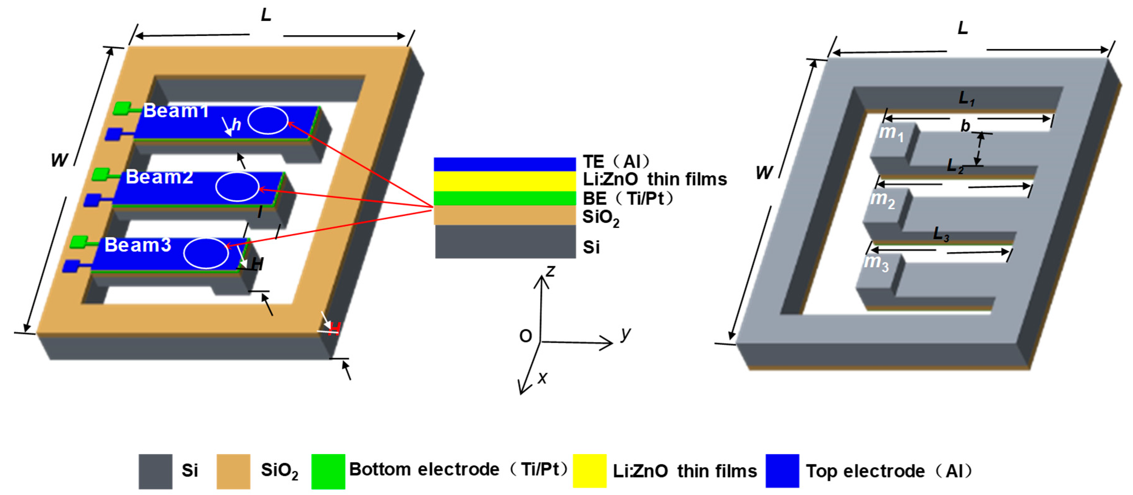
2.1. Basic Structure
2.2. Working Principle
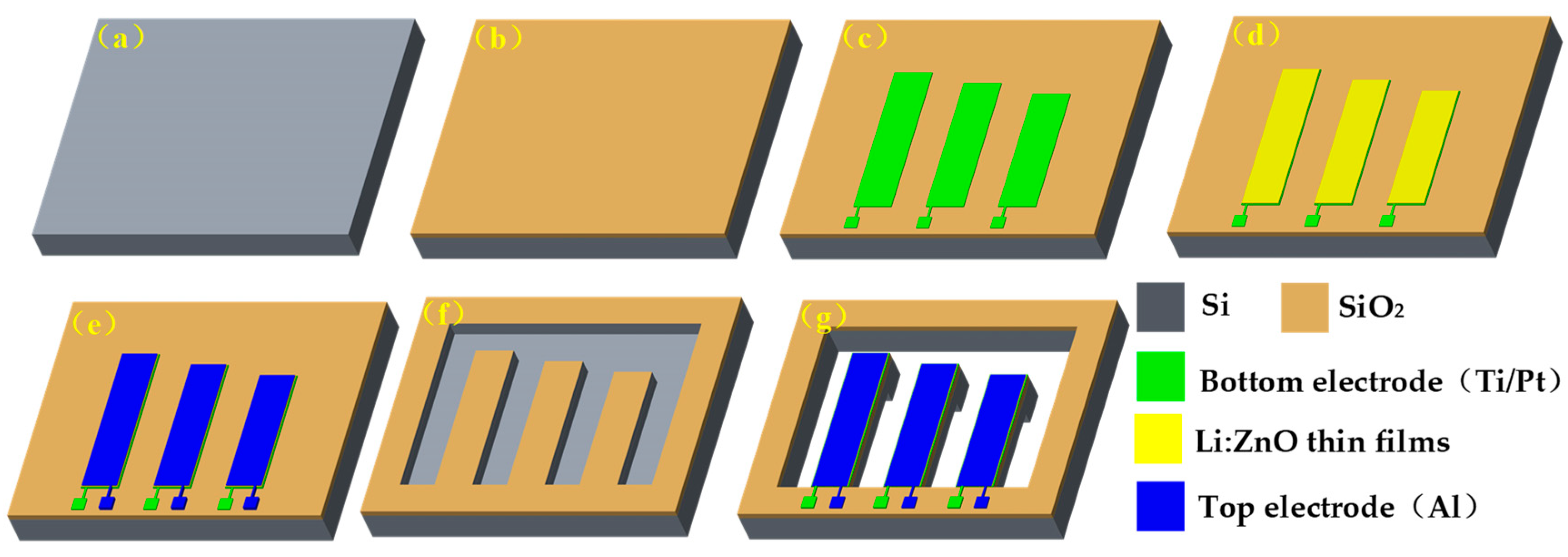
3. Fabrication Technology
4. Results and Discussion
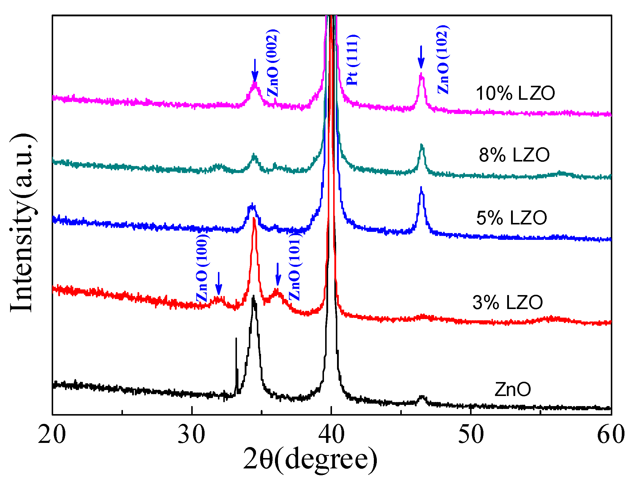
4.1. XRD Analysis
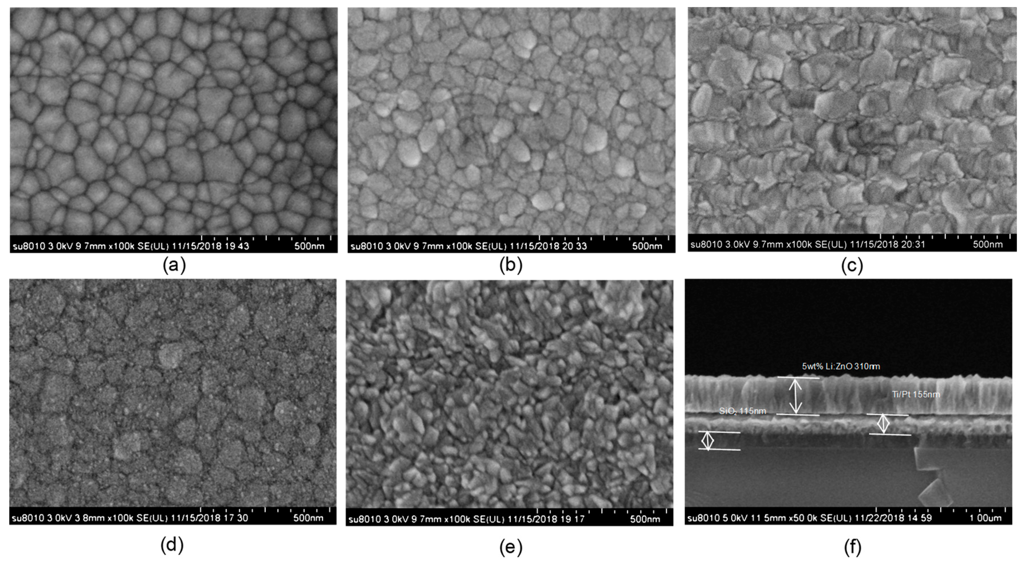
4.2. SEM Analysis
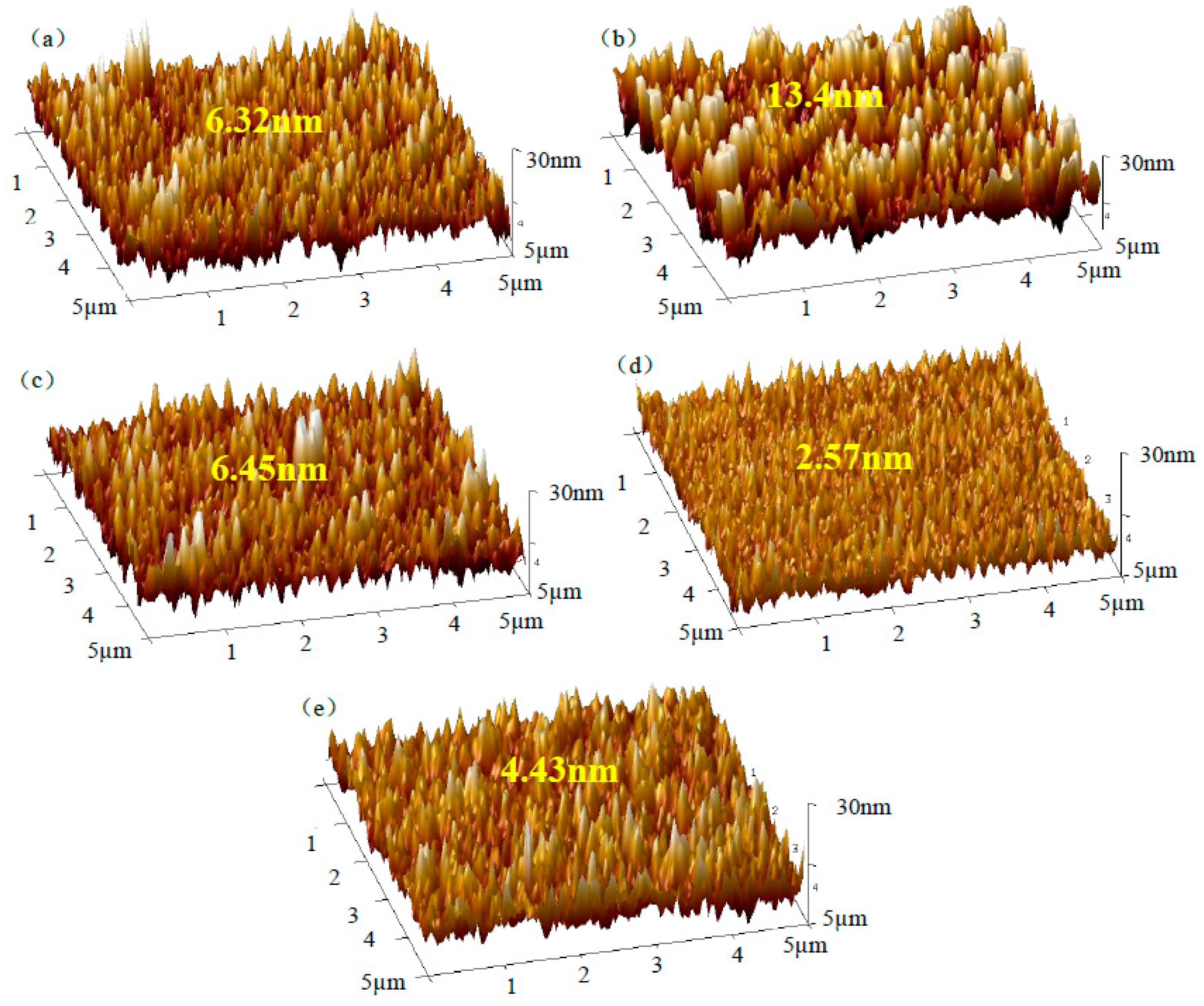
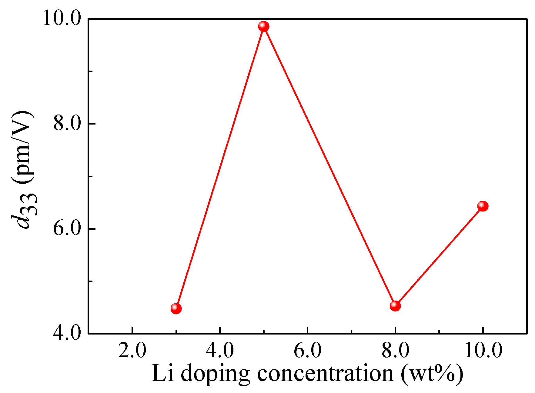
4.3. PFM Analysis
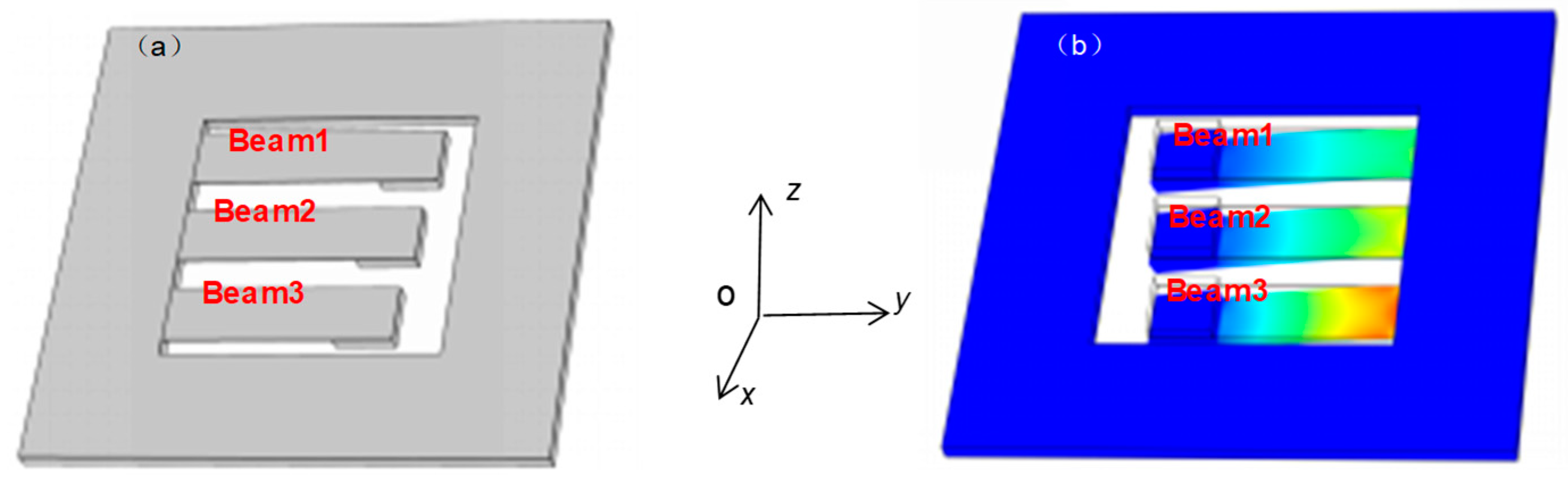
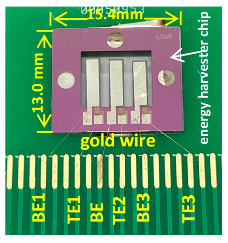
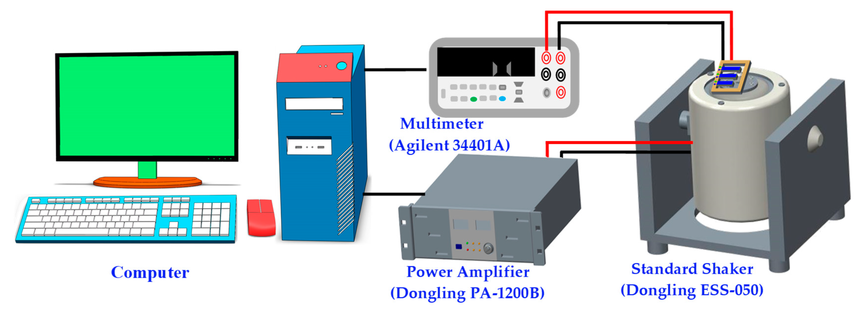
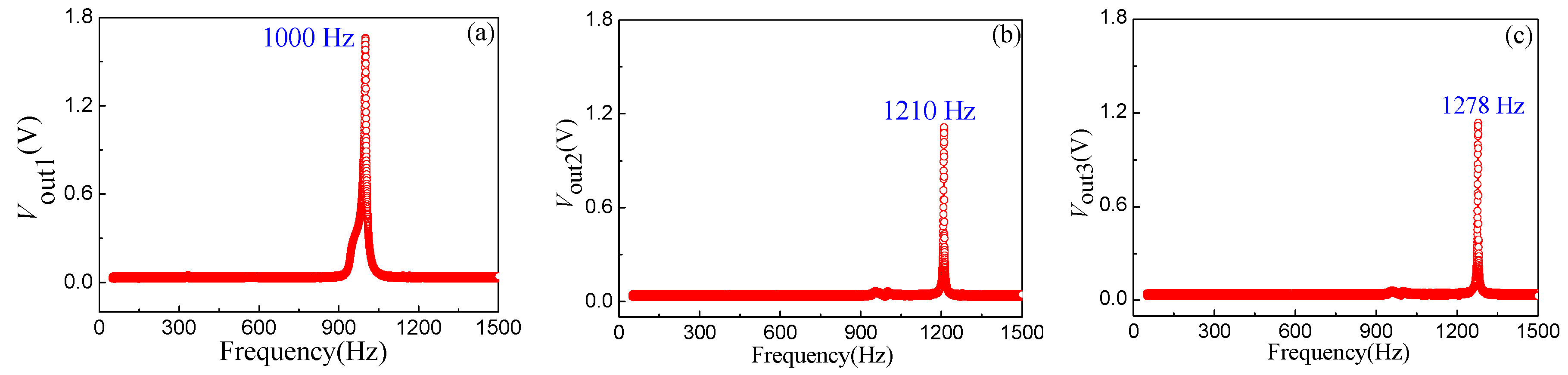
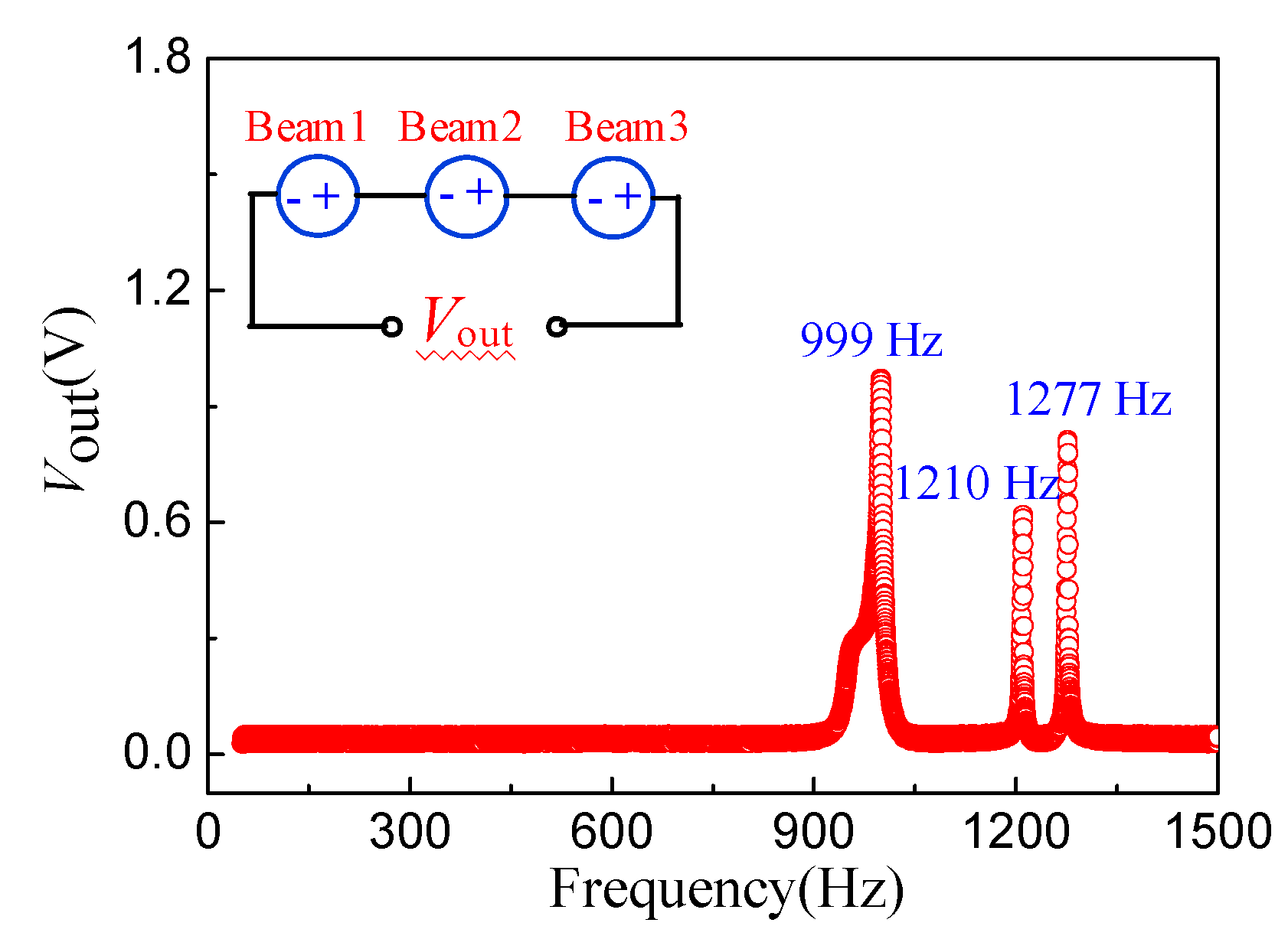
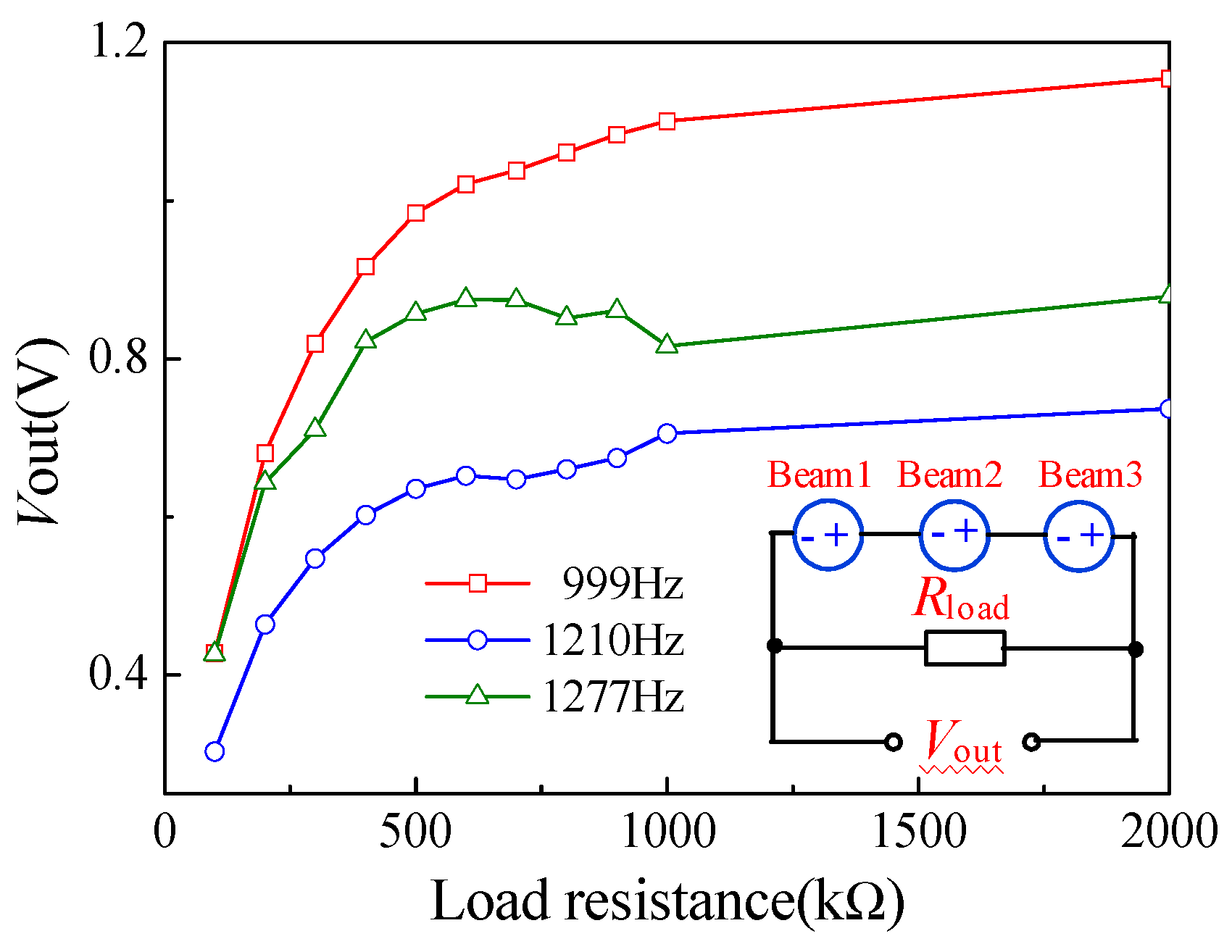
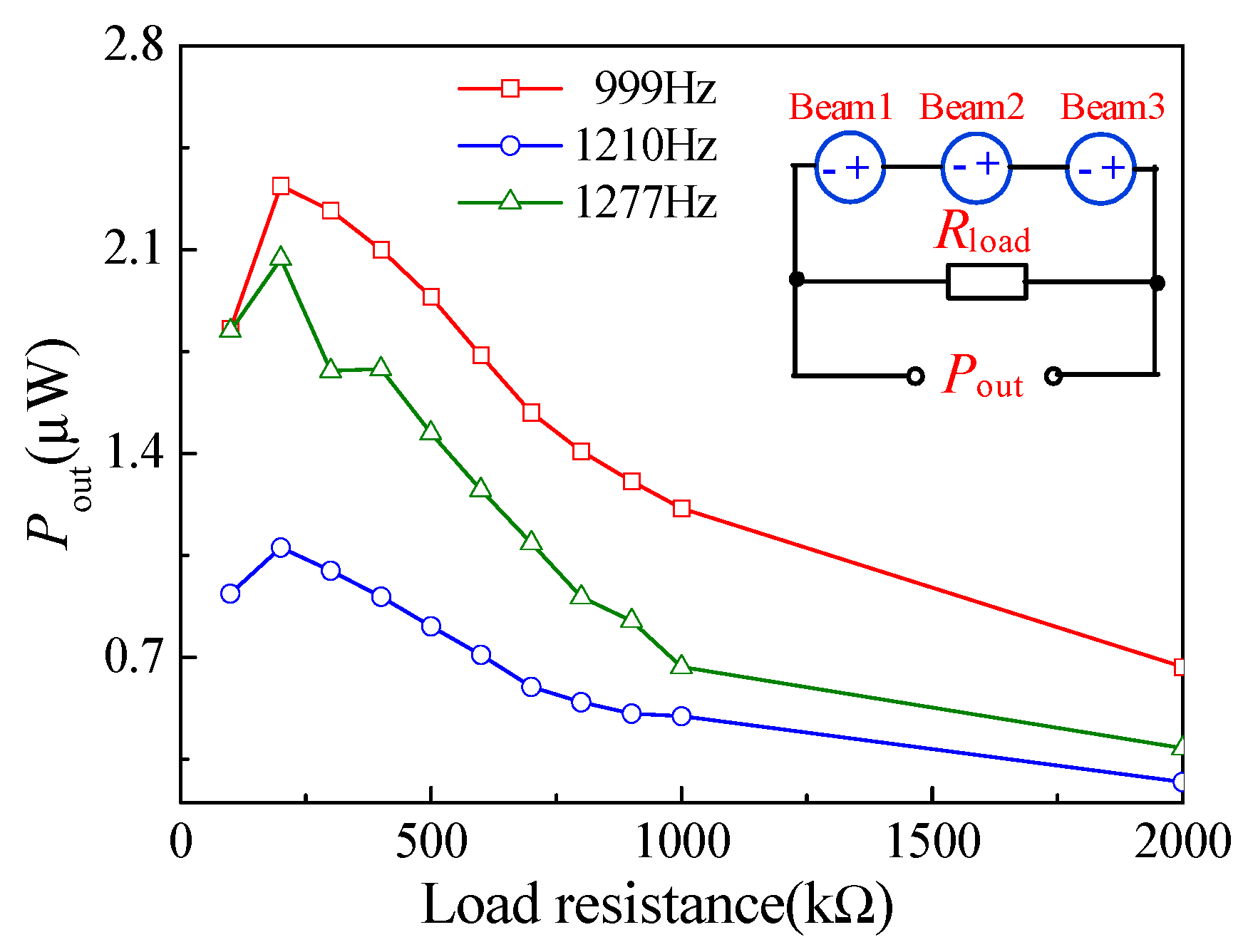
4.4. Characteristics of the Energy Harvester
5. Conclusions
Author Contributions
Funding
Conflicts of Interest
References
- Xue, H.; Hu, H.; Hu, Y.; Chen, X. An improved piezoelectric harvester available in scavenging-energy from the operating environment with either weaker or stronger vibration levels. Sci. China Ser. G Phys. Mech. Astron. 2009, 52, 218–225. [Google Scholar] [CrossRef]
- Yang, B.; Lee, C.; Xiang, W.; Xie, J.; He, J.H.; Kotlanka, R.K.; Low, S.P.; Feng, H. Electromagnetic energy harvesting from vibrations of multiple frequencies. J. Micromech. Microeng. 2009, 19, 1–8. [Google Scholar] [CrossRef]
- Edamoto, M.; Suzuki, Y.; Kasagi, N.; Kashiwagi, K.; Morizawa, Y.; Yokoyama, T.; Seki, T.; Oba, M. Low-resonant-frequency micro electret generator for energy harvestering application. In Proceedings of the 2009 IEEE 22nd International Conference on Micro Electro Mechanical Systems, Sorrento, Italy, 25–29 January 2009; Volume 978, pp. 1059–1062. [Google Scholar]
- Saadon, S.; Sidek, O. Ambient vibration-based MEMS piezoelectric energy harvester for green energy source. In Proceedings of the 2011 Fourth International Conference on Modeling, Simulation and Applied Optimization, Kuala Lumpur, Malaysia, 19–21 April 2011; Volume 978, pp. 1–6. [Google Scholar]
- Hu, Y.C.; Lee, T.H.; Chang, P.Z.; Su, P.C. High power Co3O4/ZnO p-n type piezoelectric transducer. Thin Solid Films 2015, 584, 112–115. [Google Scholar] [CrossRef]
- Janphuang, P.; Lockhart, R.; Uffer, N.; Briand, D.; de Rooij, N.F. Vibrational piezoelectric energy harvesters based on thinned bulk PZT sheets fabricated at wafer level. Sens. Actuators A 2014, 210, 1–9. [Google Scholar] [CrossRef]
- Shahruz, S.M. Design of mechanical band-pass filters with large frequency bands for energy scavenging. J. Mechatron. 2006, 16, 523–531. [Google Scholar] [CrossRef]
- Jia, Y.; Yan, J.; Soga, K.; Seshia, A.A. Multi-frequency operation of a MEMS vibration energy harvester by accessing five orders of parametric resonance. J. Phys. Conf. Ser. 2013, 476, 012126. [Google Scholar] [CrossRef]
- Nelatury, S.R.; Gray, R. MEMS electromagnetic energy harvesters with multiple resonances. Proc. SPIE 2014, 9115. [Google Scholar] [CrossRef]
- Wu, M.; Ou, Y.; Mao, H.; Li, Z.; Liu, R.; Ming, A.; Ou, W. Multi-resonant wideband energy harvester based on a folded asymmetric M-shaped cantilever. AIP Adv. 2015, 5, 077149. [Google Scholar] [CrossRef]
- Wang, P.H.; Du, H.J. ZnO thin film piezoelectric MEMS vibration energy harvesters with two piezoelectric elements for higher output performance. Rev. Sci. Instrum. 2015, 86, 075002. [Google Scholar] [CrossRef] [PubMed]
- Tao, K.; Yi, H.; Tang, L.; Wu, J.; Wang, P.; Wang, N.; Hu, L.; Fu, Y.; Miao, J.; Chang, H. Piezoelectric ZnO thin films for 2DOF MEMS vibration energy harvester. Surf. Coat. Technol. 2019, 359, 289–295. [Google Scholar] [CrossRef]
- Yuan, Y.; Shyong Chow, K.; Du, H.; Wang, P.; Zhang, M.; Yu, S.; Liu, B. A ZnO thin-film driven microcantilever for nanoscale actuation and sensing. Int. J. Smart Nano Mater. 2013, 2, 128–141. [Google Scholar] [CrossRef]
- Ai, C.P.; Zhao, X.F.; Bai, Y.N.; Li, Y.; Wen, D. Fabrication and characteristic of force sensor based on piezoelectric effect of Li-doped ZnO thin films. Mod. Phys. Lett. B 2018, 32, 1850208. [Google Scholar] [CrossRef]
- Jeong, S.H.; Park, B.N.; Lee, S.B.; Boo, J.H. Study on the doping effect of Li-doped ZnO film. Thin Solid Films 2008, 516, 5586–5589. [Google Scholar] [CrossRef]
- Johny, T.A.; Kumar, V.; Imai, H.; Kanno, I. Influence of lithium doping on the structural and electrical characteristics of ZnO thin films. Thin Solid Films 2012, 520, 5797–5800. [Google Scholar] [CrossRef]
- Ralib, A.A.M.; Nordin, A.N.; Salleh, H.; Othman, R. Fabracation of aluminium doped zinc oxide piezoelectric thin film on a silicon substrate for piezoelectric MEMS energy harvesters. Microsyst. Technol. 2012, 18, 1761–1769. [Google Scholar] [CrossRef]
- Ma, Z.Q.; Zhao, W.G.; Wang, Y. Electrical properties of Na/Mg co-doped ZnO thin films. Thin Solid Fims 2007, 515, 8611–8614. [Google Scholar] [CrossRef]
- Laurenti, M.; Perrone, D.; Verna, A.; Pirri, C.; Chiolerio, A. Development of a flexible lead-free piezoelectric transducer for health monitoring in the space environment. Micromachines 2015, 6, 1729–1744. [Google Scholar] [CrossRef]
- Fortunato, M.; Chandraiahgari, C.R.; De Bellis, G.; Ballirano, P.; Soltani, P.; Kaciulis, S.; Caneve, L.; Sarto, F.; Sarto, M.S. Poezoelectric thin films of ZnO-nanorods/nanowalls grown by chemical bath deposition. IEEE Trans. Nanotechnol. 2018, 17, 311–319. [Google Scholar] [CrossRef]
- Hamid, H.M.A.; Çelik-Butler, Z. Characterization and performance analysis of Li-doped ZnO nanowire as a nano-sensor and nano-energy harvesting element. Nano Energy 2018, 50, 159–168. [Google Scholar] [CrossRef]
- Hao, J.Y.; Bai, W. Mechanics analysis of cantilever beam with uniform load. Adv. Mater. Res. 2013, 675, 98–102. [Google Scholar] [CrossRef]
- Curie, J.; Curie, P. Développement par compression de l’électricité polaire dans les cristaux hémièdres à faces inclinées. Bull. Minéral. 1880, 3–4, 90–93. [Google Scholar] [CrossRef]
- Yao, J.; Zhu, Z.Y. Piezoelectric equations and two piezoelectric sensor models. J. Vib. Eng. 2008, 21, 74–77. [Google Scholar] [CrossRef]
- Van Kampen, R.P.; Wolffenbuttel, R.F. Modeling the mechanical behavior of bulk-micromachined silicon accelerometers. Sens. Actuators A 1998, 64, 137–150. [Google Scholar] [CrossRef]
- Duff, D.G.; Edwards, P.P.; Johnson, B.F.G. Formation of a polymer-protected platinum sol: A new understanding of the parameters controlling morphology. J. Phys. Chem. 1995, 99, 15934–15944. [Google Scholar] [CrossRef]
- Chand, P.; Gaur, A.; Kumar, A.; Gaur, U.K. Structural, morphological and optical study of Li-doped ZnO thin films on Si (100) substrate deposited by pulsed laser deposition. Ceram. Int. 2014, 40, 11915–11923. [Google Scholar] [CrossRef]
- Li, S.; Zhao, X.; Bai, Y.; Li, Y.; Ai, C.; Wen, D. Fabrication technology and characteristics research of the acceleration sensor based on Li-doped ZnO piezoelectric thin films. Micromachines 2018, 9, 178. [Google Scholar] [CrossRef]
- Yasemin, C.; Mujdat, C.; Saliha, I. XRD, SEM, XPS studies of Sb doped ZnO films and electrical properties of its based Schottky diodes. Optik 2018, 164, 424–432. [Google Scholar]
- Xu, S.Y.; Poirier, G.; Yao, N. PMN-PT nanowires with a very high piezoelectric constant. Nano Lett. 2012, 12, 2238–2242. [Google Scholar] [CrossRef]
- Fang, H.B.; Liu, J.Q.; Xu, Z.Y.; Dong, L.; Wang, L.; Chen, D.; Cai, B.-C.; Liu, Y. Fabrication and performance of MEMS-based piezoelectric power generator for vibration energy harvesting. Microelectron. J. 2006, 37, 1280–1284. [Google Scholar] [CrossRef]
- Liu, H.; Tay, C.J.; Quan, C.; Kobayashi, T.; Lee, C. Piezoelectric MEMS energy harvester for low-frequency vibrations with wideband operation range and steadily increased output power. J. Microelectromechan. Syst. 2011, 5, 1131–1142. [Google Scholar] [CrossRef]
- Toyabur, R.M.; Salauddin, M.; Park, J.Y. Design and experiment of piezoelectric multimodal energy harvester for low frequency vibration. Ceram. Int. 2017, 43, S675–S681. [Google Scholar] [CrossRef]


| Structure | Piezoelectric Material | Performance | Reference | ||
|---|---|---|---|---|---|
| Resonant Frequency | Maximum Output Voltage | Maximum Output Power | |||
| Cantilever beam | AZO thin films | 7.77 MHz | 1.61 V | - | [17] |
| Cantilever beam | Co3O4/ZnO thin films | 37 Hz | - | 10.4 μW | [5] |
| Cantilever beam | ZnO thin films | 1300.1 Hz | 2.06 V | 1.25 μW | [11] |
| Beam | ZnO thin films | 403.8 Hz | 10 mV | - | [12] |
| 489.9 Hz | 15 mV | ||||
| Cantilever beam | PZT thin films | 608 Hz | 898 mV | 2.16 mW | [31] |
| Cantilever beam | PZT thin films | 36 Hz | - | 0.53 μW | [32] |
| Cantilever beam | PZT thin films | 16 Hz | - | 740 μW | [33] |
| Multi-cantilever beam | LZO thin films | 999 Hz | 1.02 V | 2.3 µW | In this work |
| 1210 Hz | - | - | |||
| 1277 Hz | - | - | |||
© 2019 by the authors. Licensee MDPI, Basel, Switzerland. This article is an open access article distributed under the terms and conditions of the Creative Commons Attribution (CC BY) license (http://creativecommons.org/licenses/by/4.0/).
Share and Cite
Zhao, X.; Li, S.; Ai, C.; Liu, H.; Wen, D. Fabrication and Characterization of the Li-Doped ZnO Thin Films Piezoelectric Energy Harvester with Multi-Resonant Frequencies. Micromachines 2019, 10, 212. https://doi.org/10.3390/mi10030212
Zhao X, Li S, Ai C, Liu H, Wen D. Fabrication and Characterization of the Li-Doped ZnO Thin Films Piezoelectric Energy Harvester with Multi-Resonant Frequencies. Micromachines. 2019; 10(3):212. https://doi.org/10.3390/mi10030212
Chicago/Turabian StyleZhao, Xiaofeng, Sen Li, Chunpeng Ai, Hongmei Liu, and Dianzhong Wen. 2019. "Fabrication and Characterization of the Li-Doped ZnO Thin Films Piezoelectric Energy Harvester with Multi-Resonant Frequencies" Micromachines 10, no. 3: 212. https://doi.org/10.3390/mi10030212
APA StyleZhao, X., Li, S., Ai, C., Liu, H., & Wen, D. (2019). Fabrication and Characterization of the Li-Doped ZnO Thin Films Piezoelectric Energy Harvester with Multi-Resonant Frequencies. Micromachines, 10(3), 212. https://doi.org/10.3390/mi10030212