Three-Dimensional Printed Piezoelectric Array for Improving Acoustic Field and Spatial Resolution in Medical Ultrasonic Imaging

 ,
, 
 ,
, 


Abstract
:1. Introduction
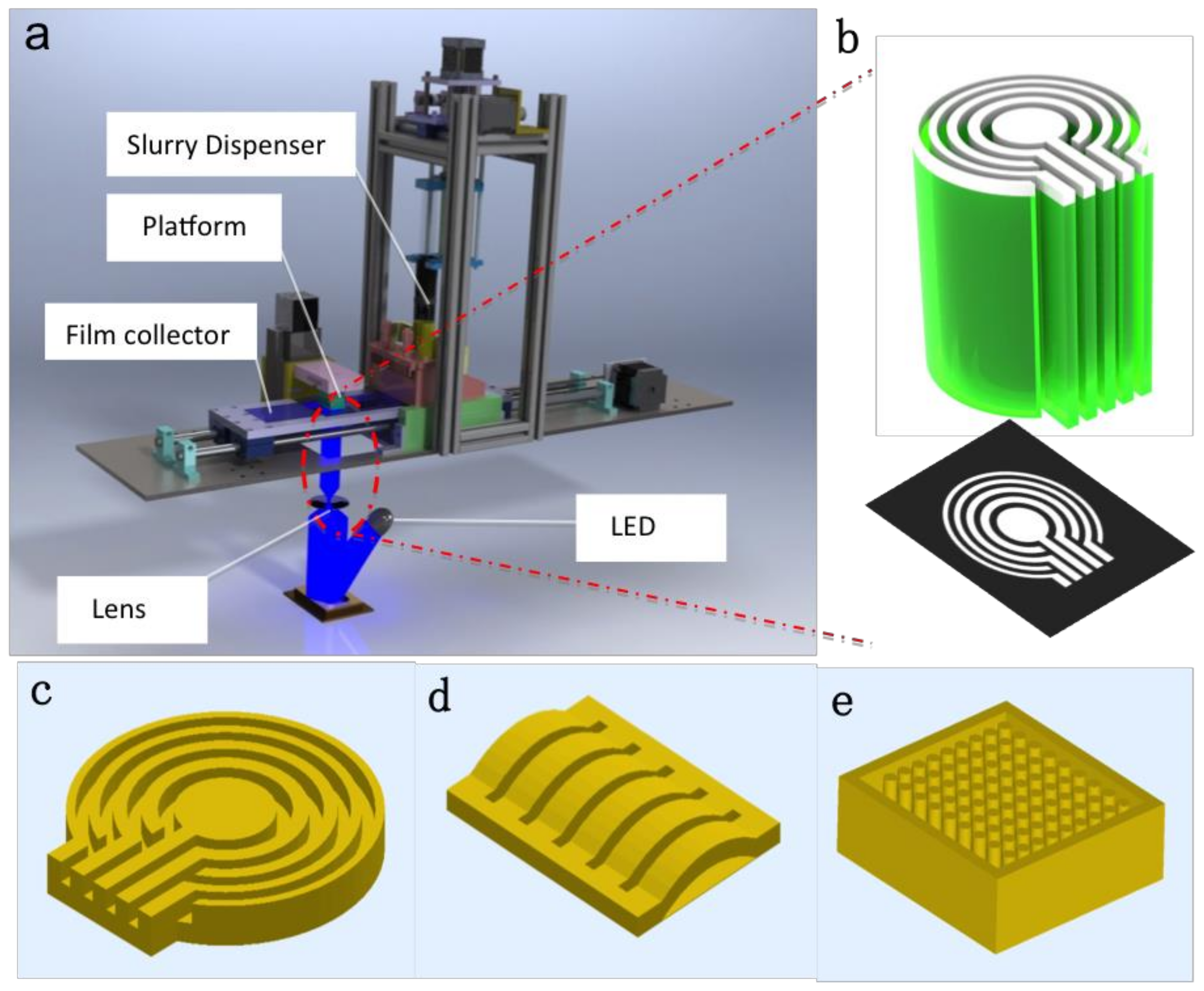
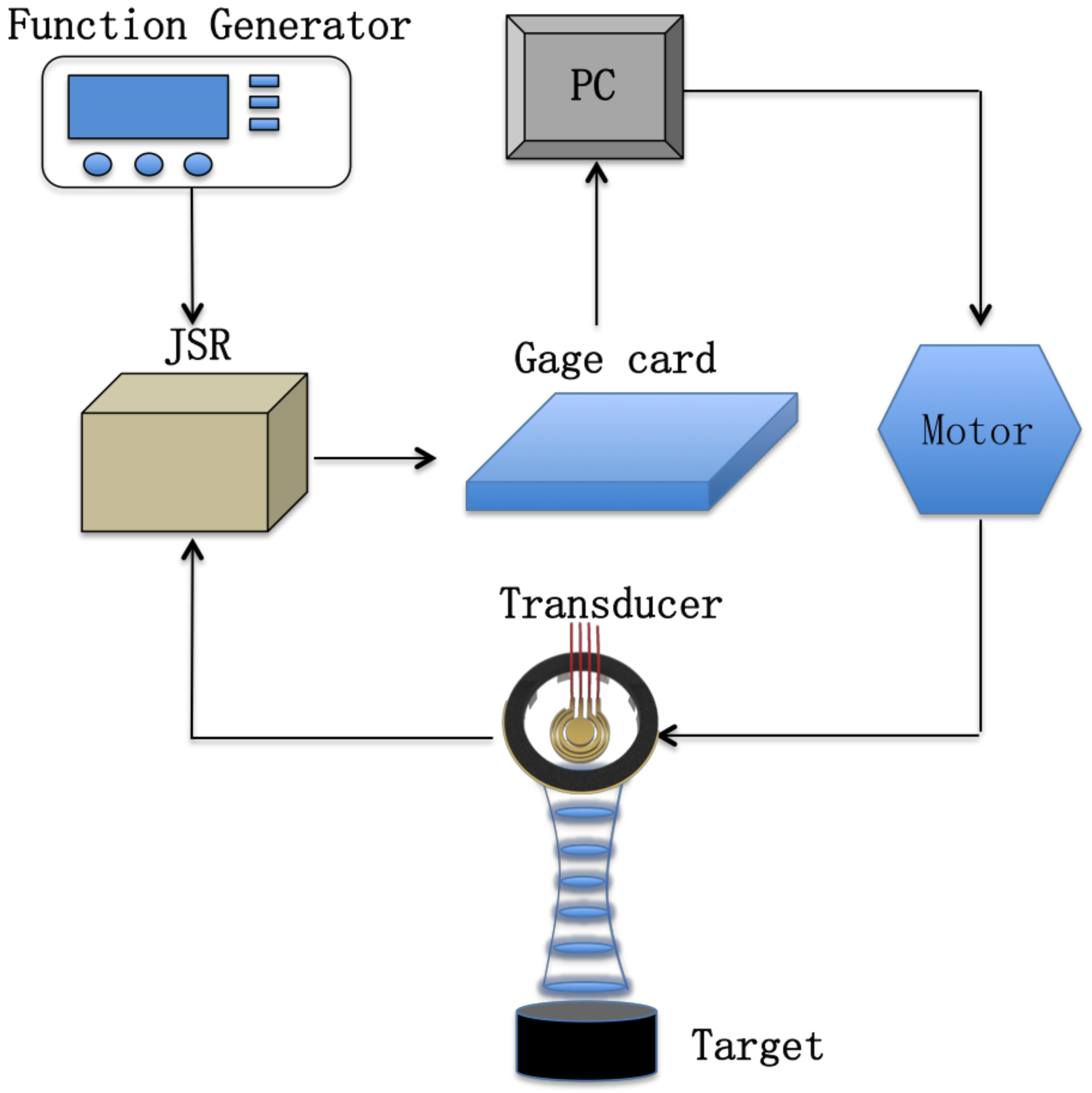
2. Materials and Methods
3. Results and Discussion
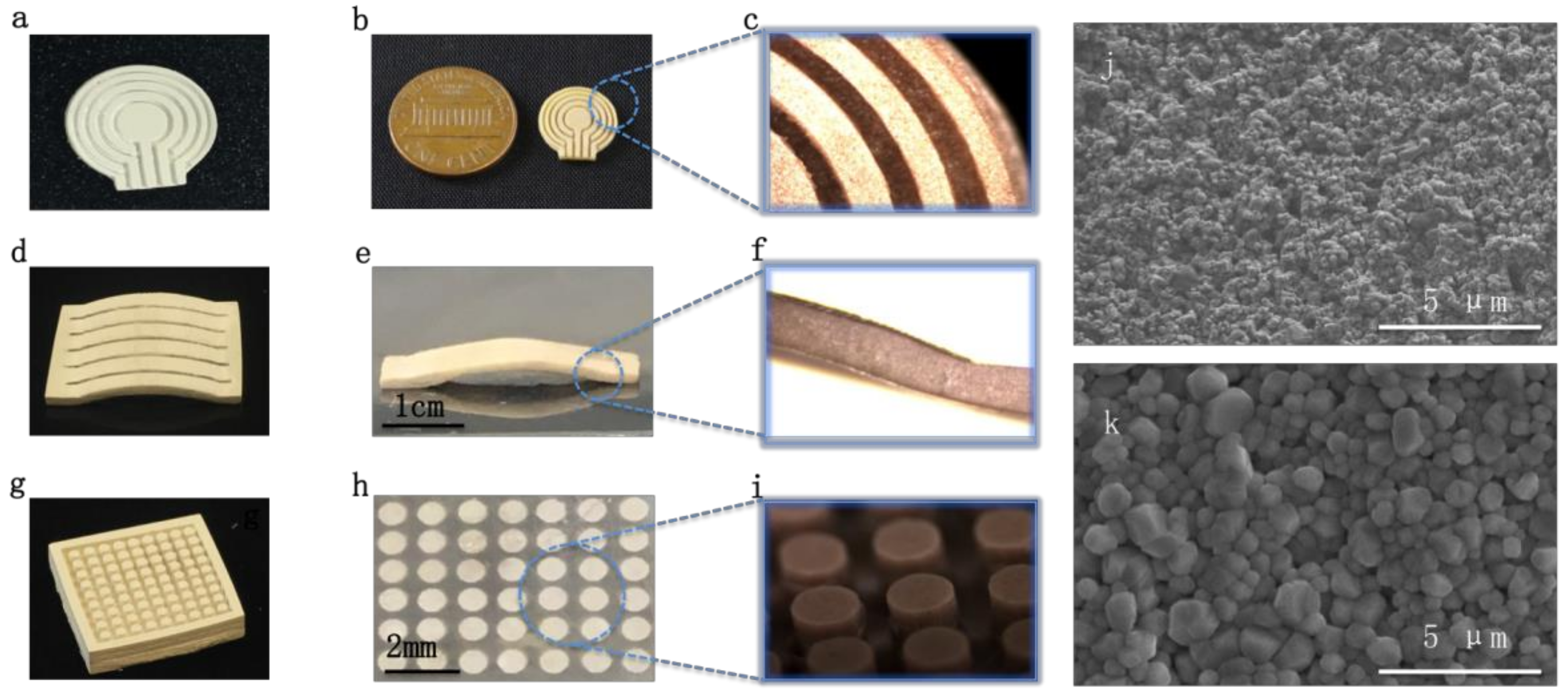
3.1. Characterization of Sintered-Parts
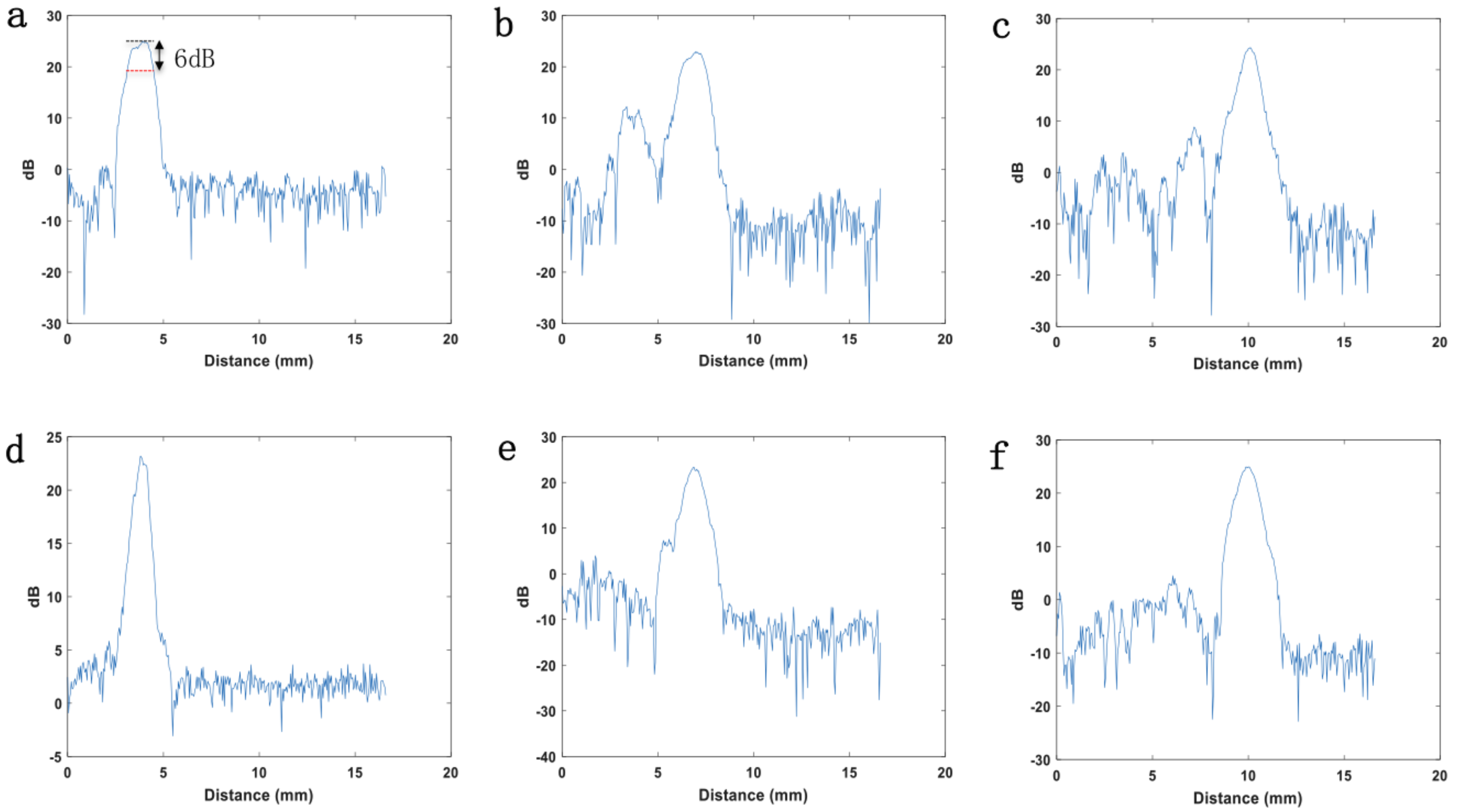
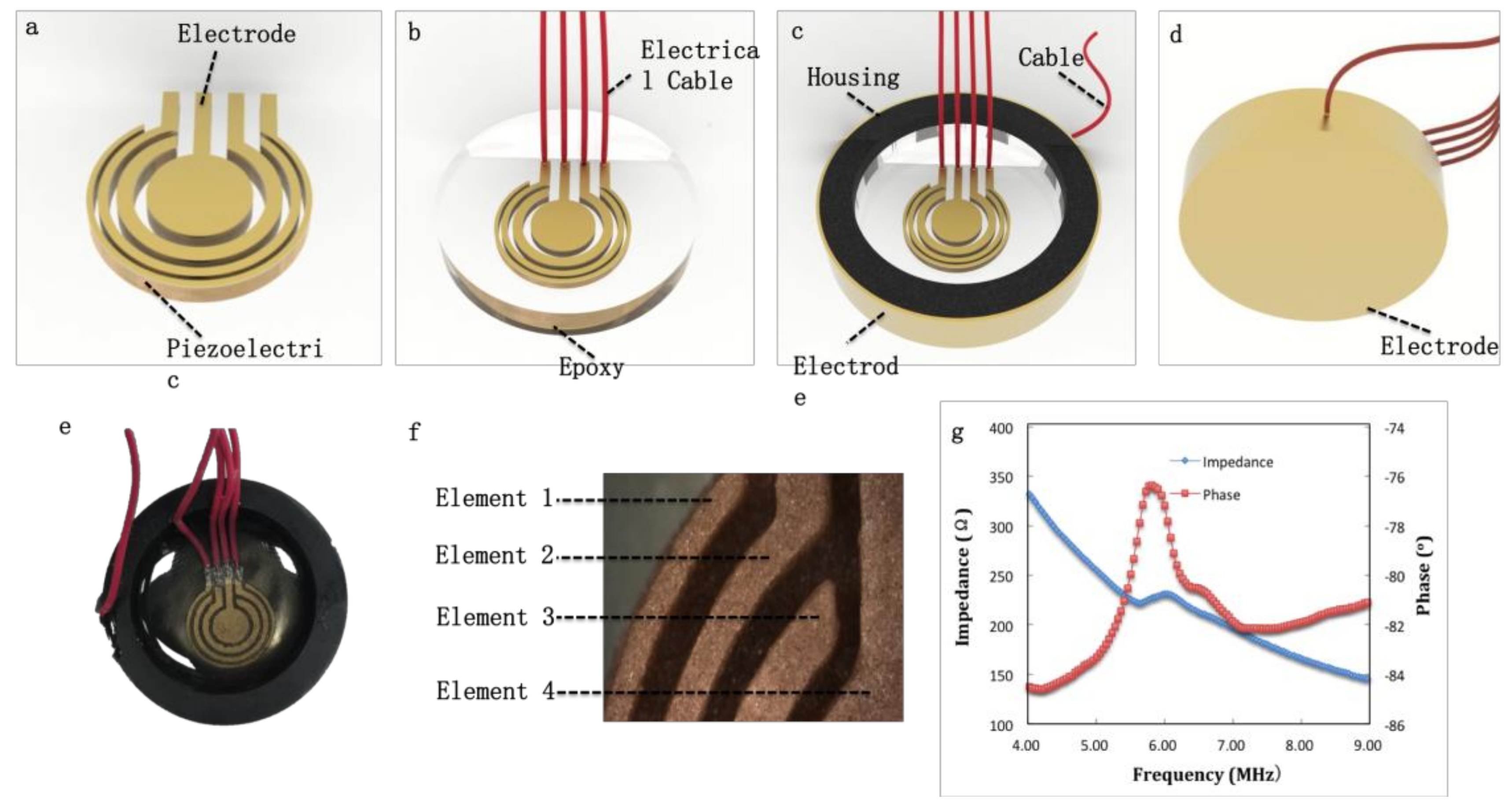
3.2. Annular Array Transducer
4. Conclusions
Author Contributions
Funding
Conflicts of Interest
References
- Dagdeviren, C.; Su, Y.; Joe, P.; Yona, R.; Liu, Y.; Kim, Y.S.; Huang, Y.; Damadoran, A.R.; Xia, J.; Martin, L.W.; et al. Conformable amplified lead zirconate titanate sensors with enhanced piezoelectric response for cutaneous pressure monitoring. Nat. Commun. 2014, 5, 4496. [Google Scholar] [CrossRef] [PubMed]
- Fan, F.R.; Tang, W.; Wang, Z.L. Flexible Nanogenerators for Energy Harvesting and Self-Powered Electronics. Adv. Mater. 2016, 28, 4283–4305. [Google Scholar] [CrossRef] [PubMed]
- Hwang, G.T.; Park, H.; Lee, J.H.; Oh, S.; Park, K.I.; Byun, M.; Park, H.; Ahn, G.; Jeong, C.K.; No, K.; et al. Self-powered cardiac pacemaker enabled by flexible single crystalline PMN-PT piezoelectric energy harvester. Adv. Mater. 2014, 26, 4880–4887. [Google Scholar] [CrossRef] [PubMed]
- Atul, S.T.; Babu, M.L. Characterization of valveless micropump for drug delivery by using piezoelectric effect. In Proceedings of the Advances in Computing, Communications and Informatics (ICACCI), Jaipur, India, 21–24 September 2016; IEEE: Piscataway, NJ, USA, 2016; pp. 2138–2144. [Google Scholar] [CrossRef]
- Chen, X.; Lam, K.h.; Chen, R.; Chen, Z.; Yu, P.; Chen, Z.; Shung, K.K.; Zhou, Q. An adjustable multi-scale single beam acoustic tweezer based on ultrahigh frequency ultrasonic transducer. Biotech. Bioeng. 2017. [Google Scholar] [CrossRef] [PubMed]
- Hu, H.; Zhu, X.; Wang, C.; Zhang, L.; Li, X.; Lee, S.; Huang, Z.; Chen, R.; Chen, Z.; Wang, C. Stretchable ultrasonic transducer arrays for three-dimensional imaging on complex surfaces. Sci. Adv. 2018, 4, eaar3979. [Google Scholar] [CrossRef] [PubMed]
- Kennedy, J.E. High-intensity focused ultrasound in the treatment of solid tumours. Nat. Rev. Cancer 2005, 5, 321. [Google Scholar] [CrossRef] [PubMed]
- Dziewierz, J.; Ramadas, S.; Gachagan, A.; O’Leary, R.; Hayward, G. A 2D Ultrasonic Array design incorporating Hexagonal-shaped Elements and Triangular-cut Piezocomposite Substructure for NDE applications. In Proceedings of the Ultrasonics Symposium (IUS), Rome, Italy, 20–23 September 2009; IEEE: Piscataway, NJ, USA, 2009; pp. 422–425. [Google Scholar]
- Lee, H.J.; Zhang, S.; Bar-Cohen, Y.; Sherrit, S. High temperature, high power piezoelectric composite transducers. Sensors 2014, 14, 14526–14552. [Google Scholar] [CrossRef] [PubMed]
- He, L.; Yang, H.; Zhou, D.; Niu, Y.; Xiang, F.; Wang, H. Improved dielectric and magnetic properties of 1–3-type Ni0. 5Zn0. 5Fe2O4/epoxy composites for high-frequency applications. J. Phys. D 2013, 46, 125003. [Google Scholar] [CrossRef]
- Lee, D.H.; Derby, B. Preparation of PZT suspensions for direct ink jet printing. J. Eur. Ceram. Soc. 2004, 24, 1069–1072. [Google Scholar] [CrossRef]
- Lewis, J.A. Direct ink writing of 3D functional materials. Adv. Funct. Mater. 2006, 16, 2193–2204. [Google Scholar] [CrossRef]
- Özkol, E.; Wätjen, A.M.; Bermejo, R.; Deluca, M.; Ebert, J.; Danzer, R.; Telle, R. Mechanical characterisation of miniaturised direct inkjet printed 3Y-TZP specimens for microelectronic applications. J. Eur. Ceram. Soc. 2010, 30, 3145–3152. [Google Scholar] [CrossRef]
- Smay, J.E.; Cesarano, J.; Lewis, J.A. Colloidal inks for directed assembly of 3-D periodic structures. Langmuir 2002, 18, 5429–5437. [Google Scholar] [CrossRef]
- Franco, J.; Hunger, P.; Launey, M.E.; Tomsia, A.P.; Saiz, E. Direct write assembly of calcium phosphate scaffolds using a water-based hydrogel. Acta Biomat. 2010, 6, 218–228. [Google Scholar] [CrossRef] [PubMed]
- Sun, J.; Ngernchuklin, P.; Vittadello, M.; Akdoğan, E.; Safari, A. Development of 2-2 piezoelectric ceramic/polymer composites by direct-write technique. J. Electroceram. 2010, 24, 219–225. [Google Scholar] [CrossRef]
- Yang, H.; Yang, S.; Chi, X.; Evans, J.R. Fine ceramic lattices prepared by extrusion freeforming. J. Biomed. Mater. Res. Part B 2006, 79, 116–121. [Google Scholar] [CrossRef] [PubMed]
- Griffith, M.L. Stereolithography of ceramics. PhD Thesis, University of Michigan, Ann Arbor, MI, USA, 1995. [Google Scholar]
- O’connor, K.F.; Nohns, D.C.; Chattin, W.A. Method of combining metal and ceramic inserts into stereolithography components. U.S. Patent No. 5705117, 1998. [Google Scholar]
- Zhang, X.; Jiang, X.; Sun, C. Micro-stereolithography of polymeric and ceramic microstructures. Sens. Actuators A 1999, 77, 149–156. [Google Scholar] [CrossRef]
- Song, X.; Zhang, Z.; Chen, Z.; Chen, Y. Porous Structure Fabrication Using a Stereolithography-Based Sugar Foaming Method. J Manufact. Sci. Eng. 2017, 139, 031015. [Google Scholar] [CrossRef]
- Yang, Y.; Chen, Z.; Song, X.; Zhang, Z.; Zhang, J.; Shung, K.K.; Zhou, Q.; Chen, Y. Biomimetic anisotropic reinforcement architectures by electrically assisted nanocomposite 3D printing. Adv. Mater. 2017, 29. [Google Scholar] [CrossRef] [PubMed]
- Yang, Y.; Chen, Z.; Song, X.; Zhu, B.; Hsiai, T.; Wu, P.-I.; Xiong, R.; Shi, J.; Chen, Y.; Zhou, Q. Three dimensional printing of high dielectric capacitor using projection based stereolithography method. Nano Energy 2016, 22, 414–421. [Google Scholar] [CrossRef]
- Song, X.; Chen, Z.; Lei, L.; Shung, K.; Zhou, Q.; Chen, Y. Piezoelectric component fabrication using projection-based stereolithography of barium titanate ceramic suspensions. Rapid Prototyping J. 2017, 23, 44–53. [Google Scholar] [CrossRef]
- Chen, Z.; Song, X.; Lei, L.; Chen, X.; Fei, C.; Chiu, C.T.; Qian, X.; Ma, T.; Yang, Y.; Shung, K. 3D printing of piezoelectric element for energy focusing and ultrasonic sensing. Nano Energy 2016, 27, 78–86. [Google Scholar] [CrossRef]
- Cannata, J.M.; Ritter, T.A.; Chen, W.-H.; Silverman, R.H.; Shung, K.K. Design of efficient, broadband single-element (20-80 MHz) ultrasonic transducers for medical imaging applications. IEEE Trans. Ultrason. Ferroelectr. Freq. Control 2003, 50, 1548–1557. [Google Scholar] [CrossRef] [PubMed]
- Krause, M.; Mielentz, F.; Milman, B.; Müller, W.; Schmitz, V.; Wiggenhauser, H. Ultrasonic imaging of concrete members using an array system. NDT E Int. 2001, 34, 403–408. [Google Scholar] [CrossRef]
- Kim, T.; Kim, J.; Dalmau, R.; Schlesser, R.; Preble, E.; Jiang, X. High-temperature electromechanical characterization of AlN single crystals. IEEE Trans. Ultrason. Ferroelectr. Freq. Control 2015, 62, 1880–1887. [Google Scholar] [CrossRef] [PubMed]
- Ketterling, J.A.; Filoux, E. Synthetic-focusing strategies for real-time annular-array imaging. IEEE Trans. Ultrason. Ferroelectr. Freq. Control 2012, 59, 1830–1839. [Google Scholar] [CrossRef] [PubMed]


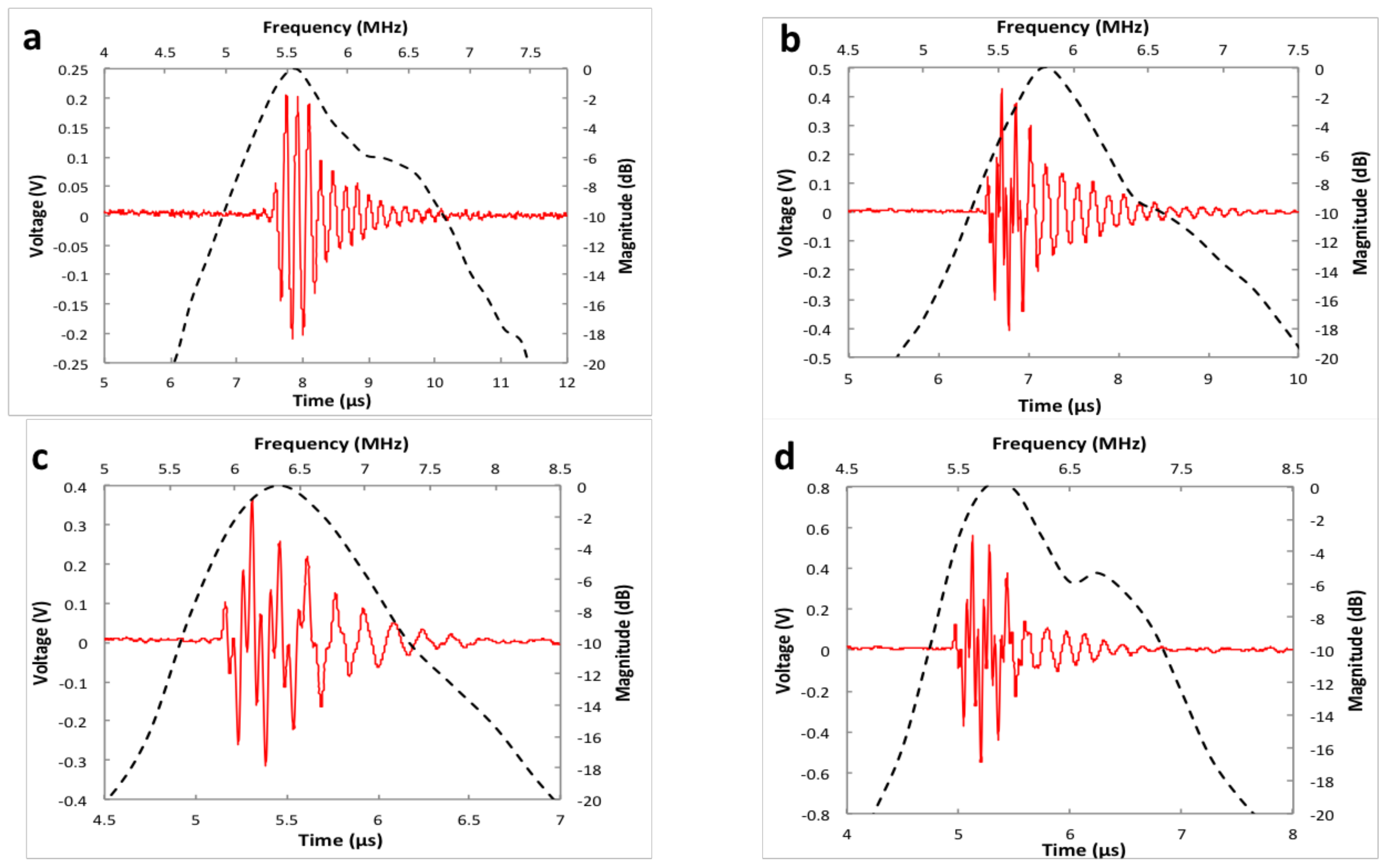
| Characteristics | Element 1 | Element 2 | Element 3 | Element 4 |
|---|---|---|---|---|
| Center Frequency (MHz) | 5.72 | 5.86 | 6.39 | 6.12 |
| −6 dB Bandwidth (%) | 19.6 | 12.9 | 19.8 | 23.6 |
| Vpp (mV) | 402 | 793 | 626 | 1039 |
| −20 dB Pulse Length (ns) | 1940 | 1621 | 989 | 2949 |
| Area (mm2) | 13.7 | 13.2 | 13.6 | 13.5 |
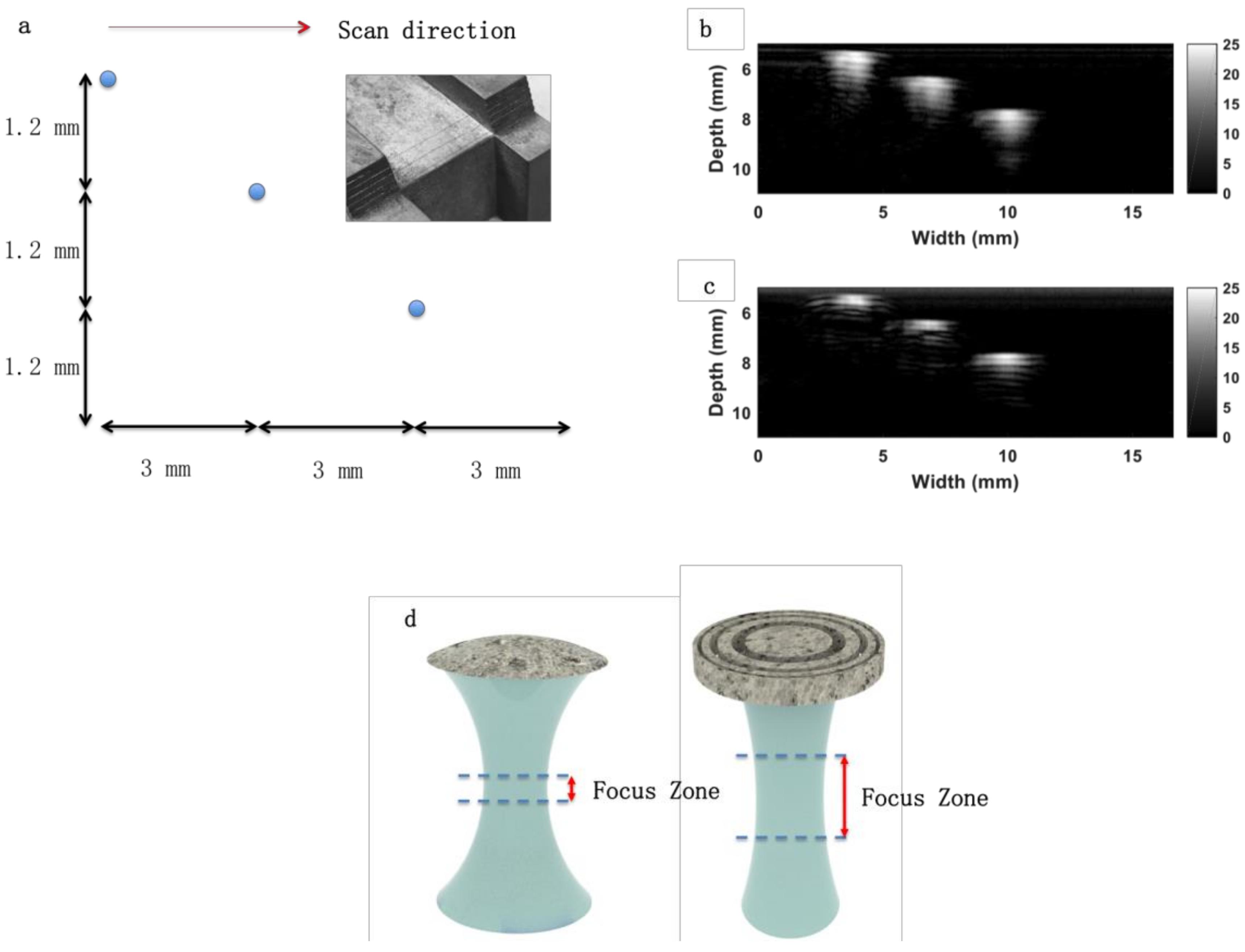
| Depth (mm) | Resolution (mm) | |
|---|---|---|
| Single Element | Annular Array | |
| 5.6 | 1.4 | 1 |
| 6.8 | 1.5 | 1.05 |
| 8 | 1.1 | 1.1 |
© 2019 by the authors. Licensee MDPI, Basel, Switzerland. This article is an open access article distributed under the terms and conditions of the Creative Commons Attribution (CC BY) license (http://creativecommons.org/licenses/by/4.0/).
Share and Cite
Chen, Z.; Qian, X.; Song, X.; Jiang, Q.; Huang, R.; Yang, Y.; Li, R.; Shung, K.; Chen, Y.; Zhou, Q. Three-Dimensional Printed Piezoelectric Array for Improving Acoustic Field and Spatial Resolution in Medical Ultrasonic Imaging. Micromachines 2019, 10, 170. https://doi.org/10.3390/mi10030170
Chen Z, Qian X, Song X, Jiang Q, Huang R, Yang Y, Li R, Shung K, Chen Y, Zhou Q. Three-Dimensional Printed Piezoelectric Array for Improving Acoustic Field and Spatial Resolution in Medical Ultrasonic Imaging. Micromachines. 2019; 10(3):170. https://doi.org/10.3390/mi10030170
Chicago/Turabian StyleChen, Zeyu, Xuejun Qian, Xuan Song, Qiangguo Jiang, Rongji Huang, Yang Yang, Runze Li, Kirk Shung, Yong Chen, and Qifa Zhou. 2019. "Three-Dimensional Printed Piezoelectric Array for Improving Acoustic Field and Spatial Resolution in Medical Ultrasonic Imaging" Micromachines 10, no. 3: 170. https://doi.org/10.3390/mi10030170
APA StyleChen, Z., Qian, X., Song, X., Jiang, Q., Huang, R., Yang, Y., Li, R., Shung, K., Chen, Y., & Zhou, Q. (2019). Three-Dimensional Printed Piezoelectric Array for Improving Acoustic Field and Spatial Resolution in Medical Ultrasonic Imaging. Micromachines, 10(3), 170. https://doi.org/10.3390/mi10030170