The Research on Actuation Performance of MEMS Safety-and-Arming Device with Interlock Mechanism


Abstract
:1. Introduction
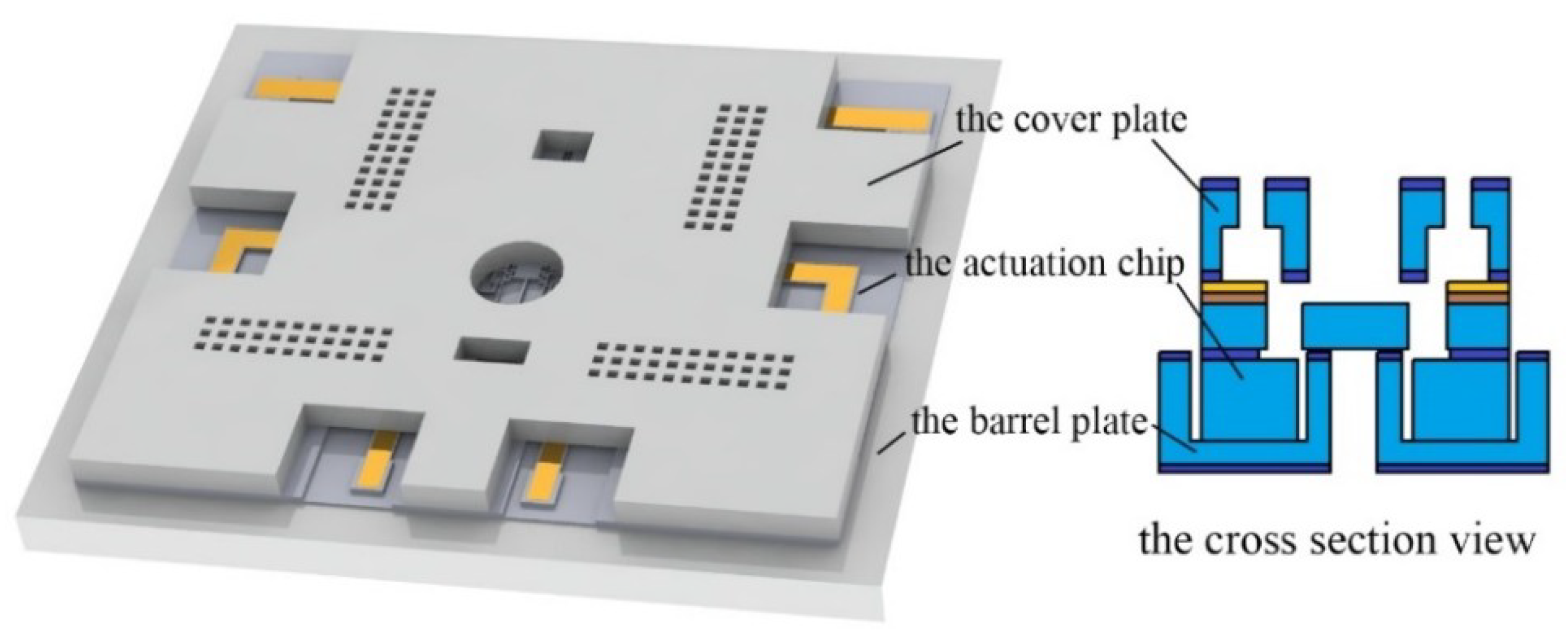
2. Modeling
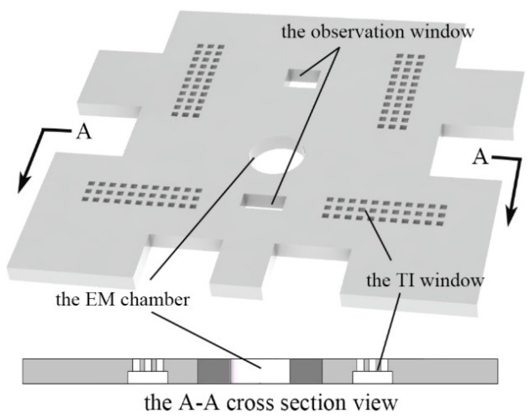
2.1. The Cover Plate
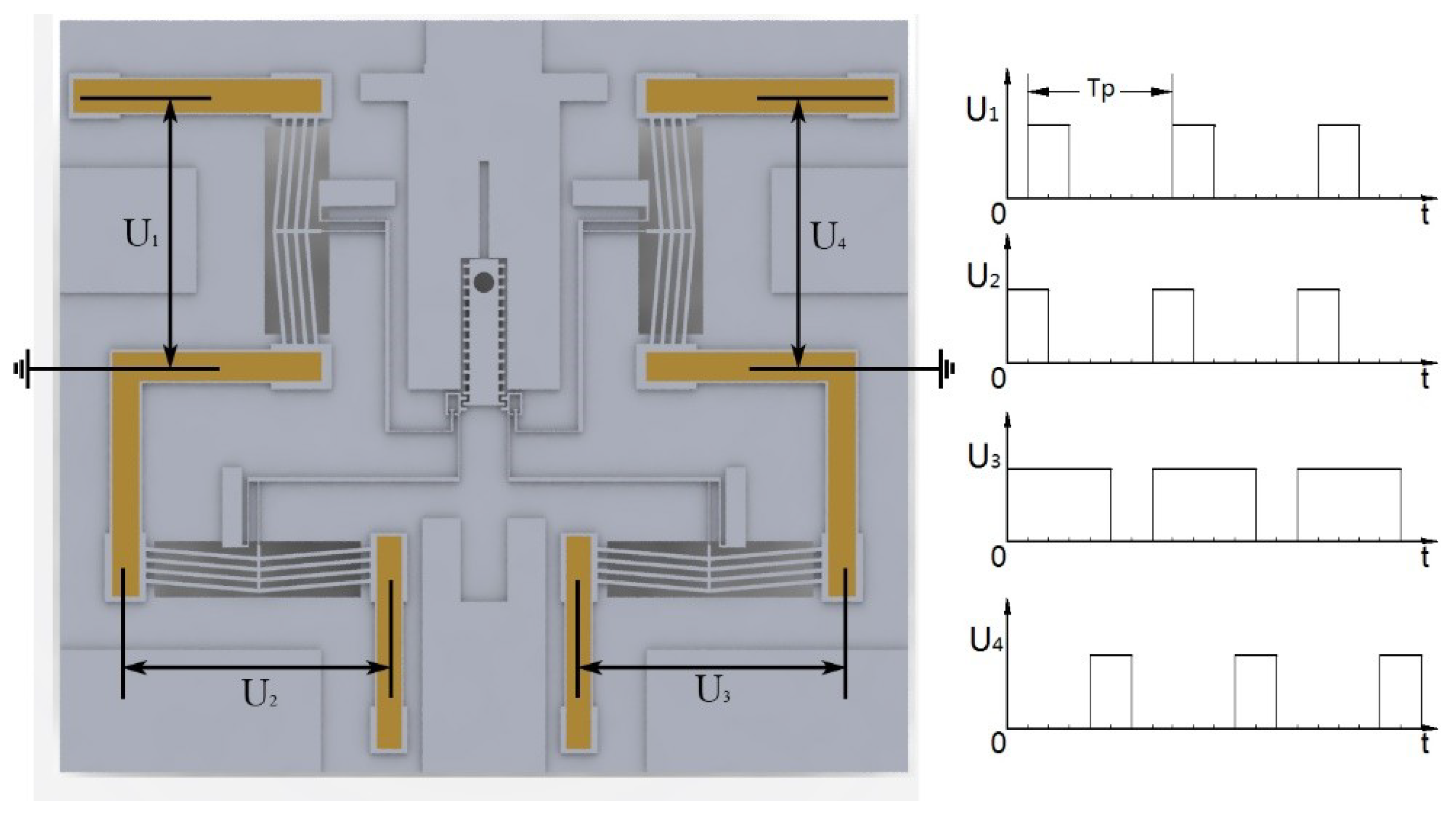
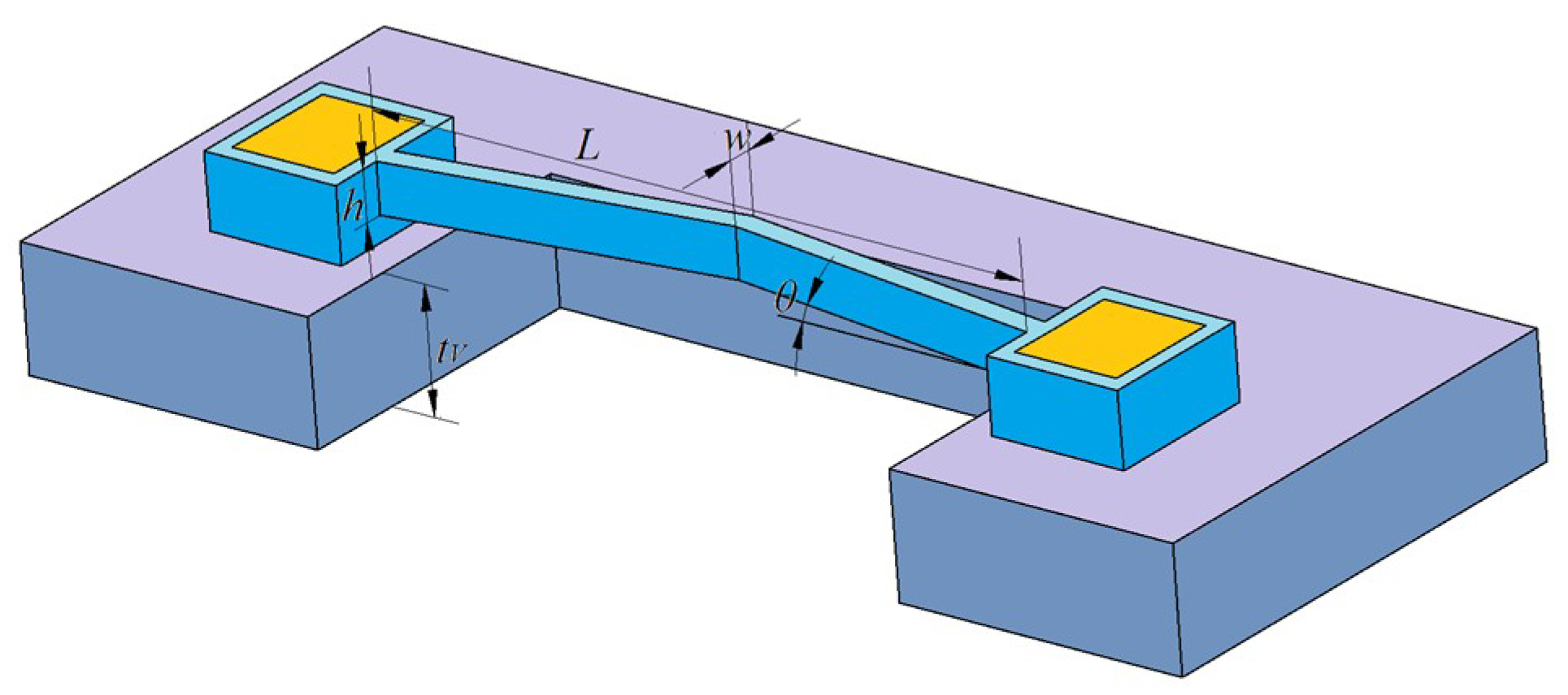
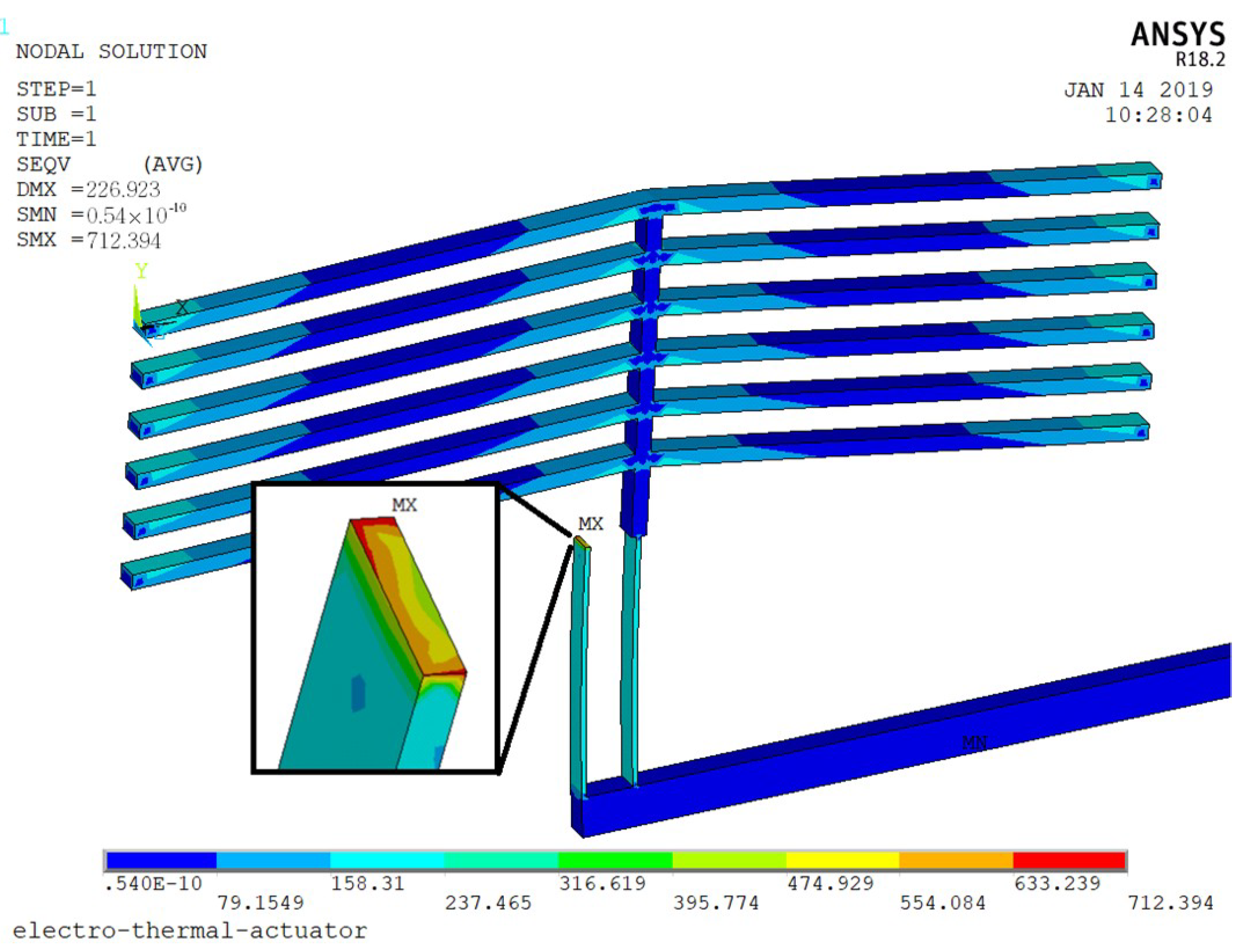
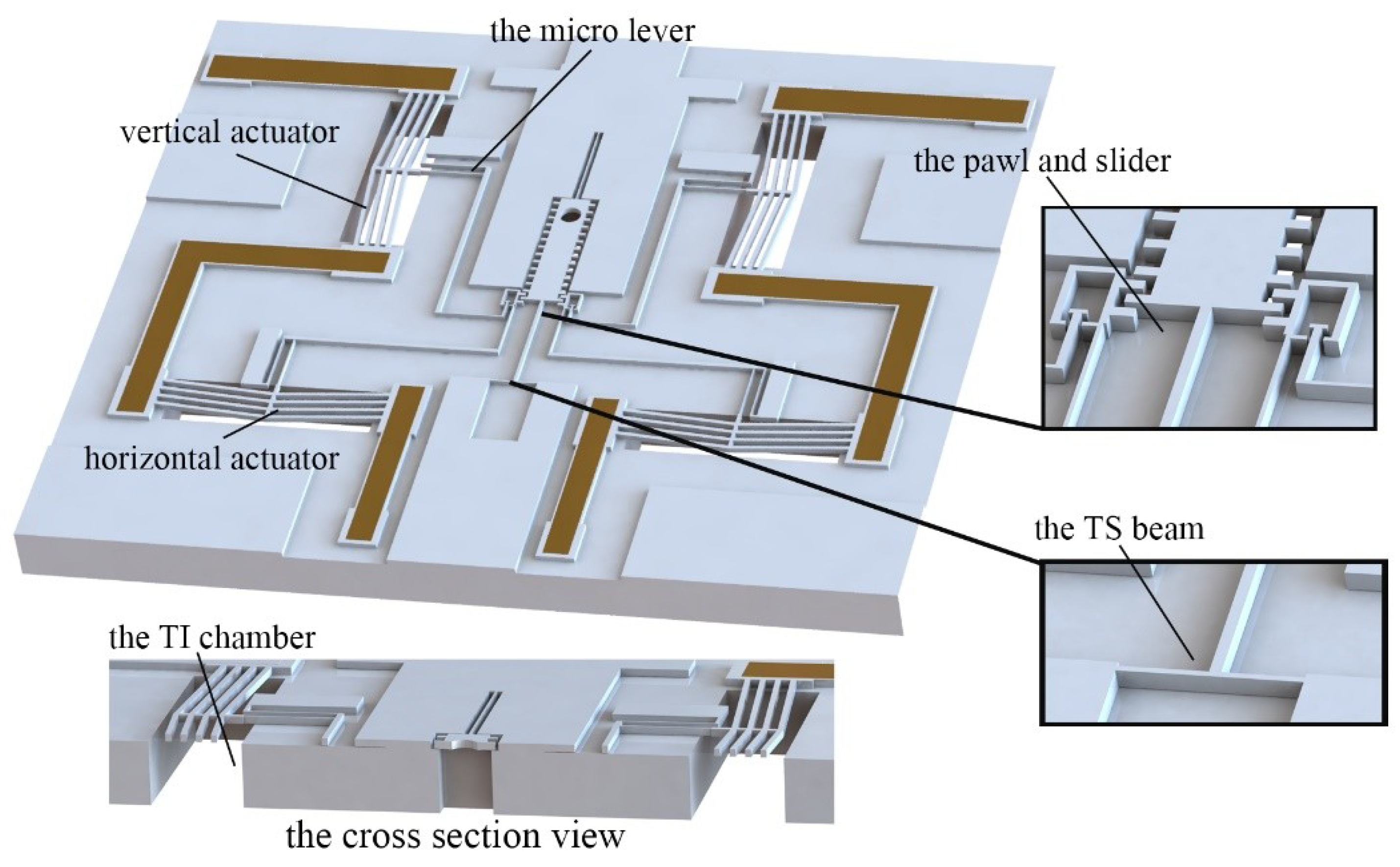
2.2. The Actuation Chip
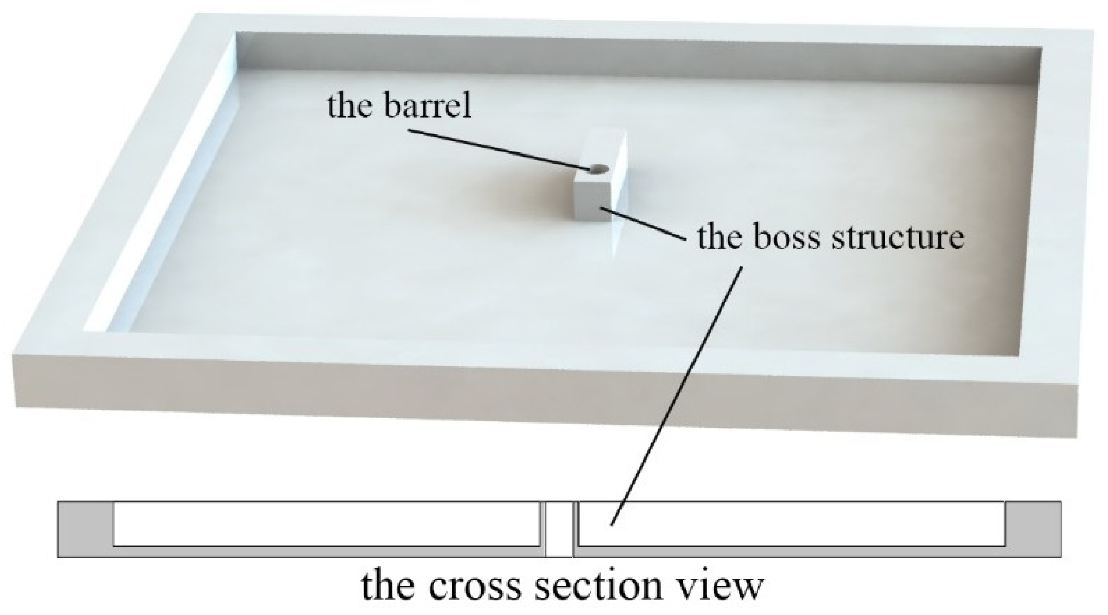
2.3. The Barrel Plate
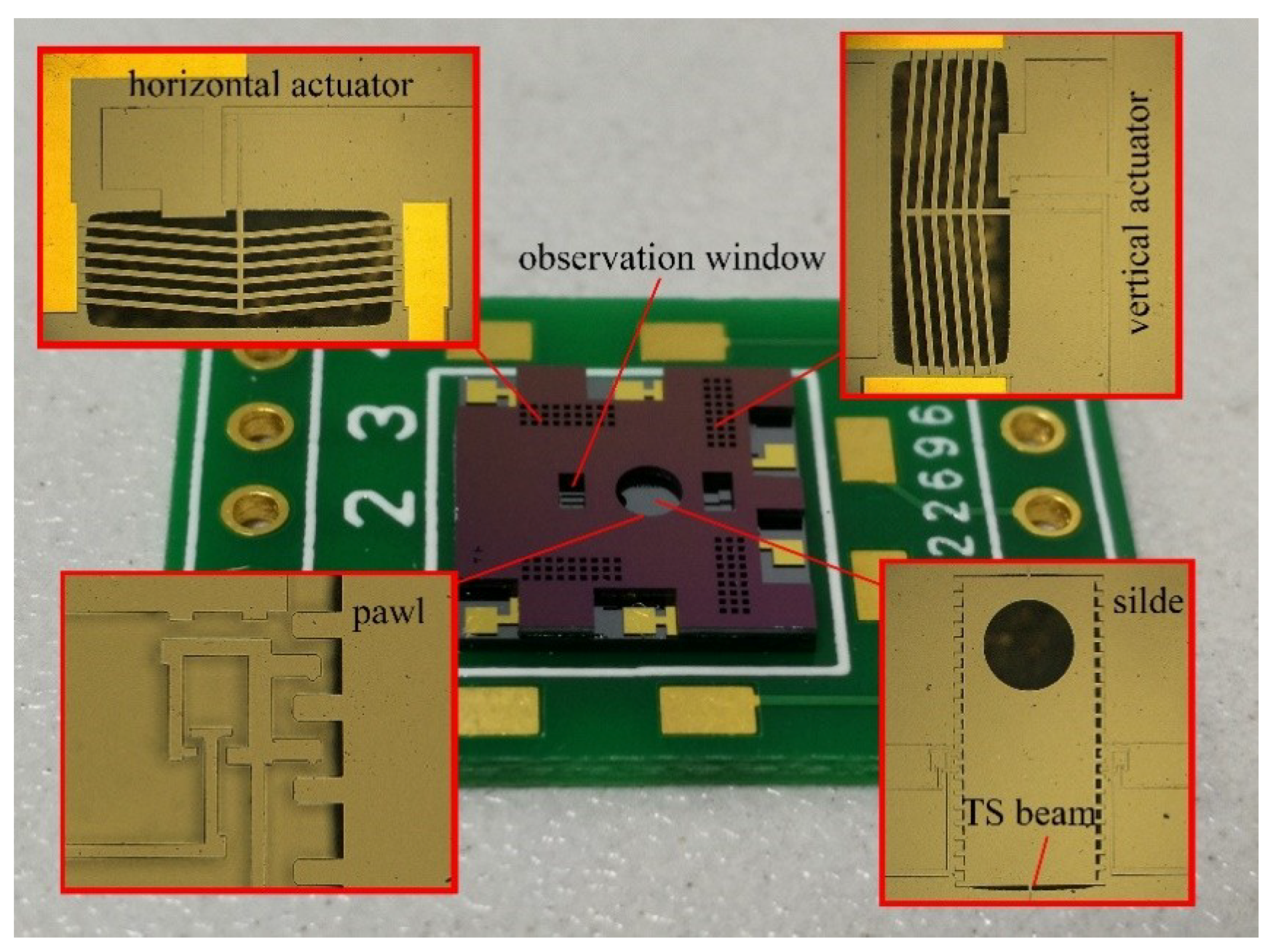
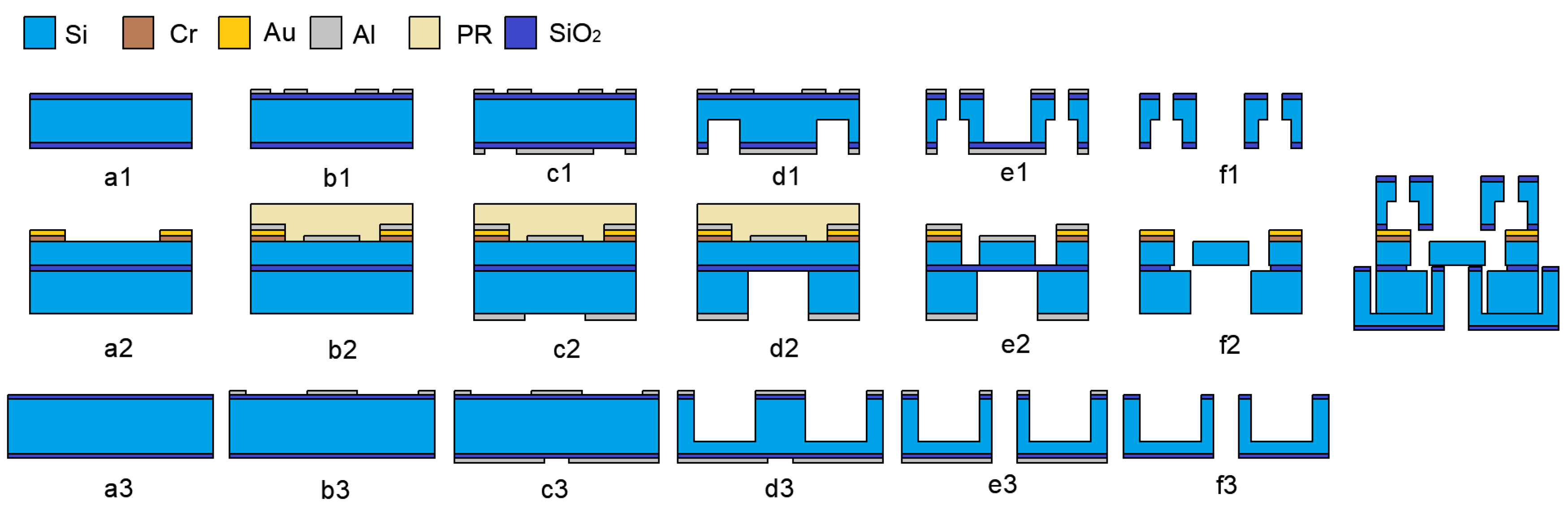
3. Fabrication Process
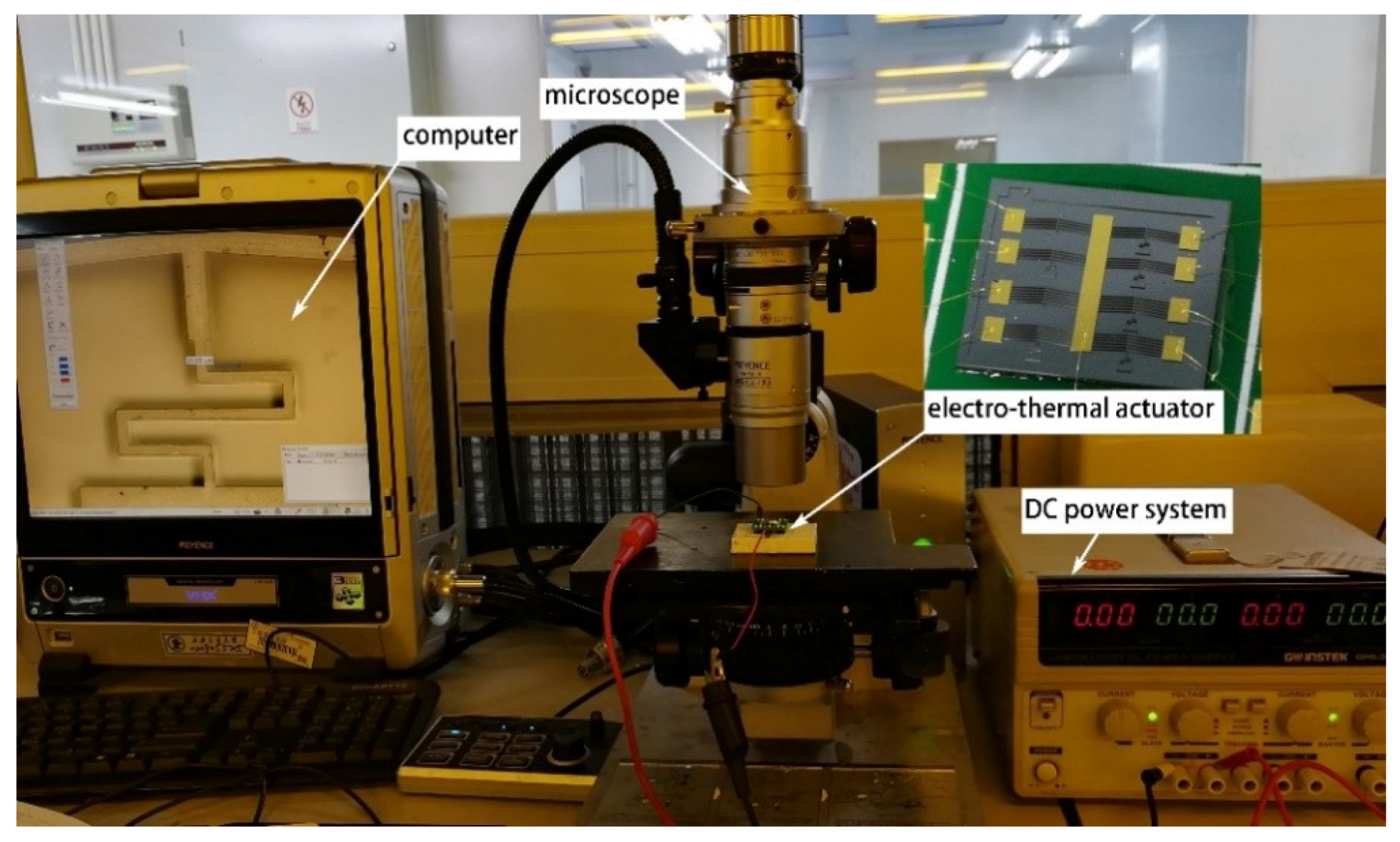
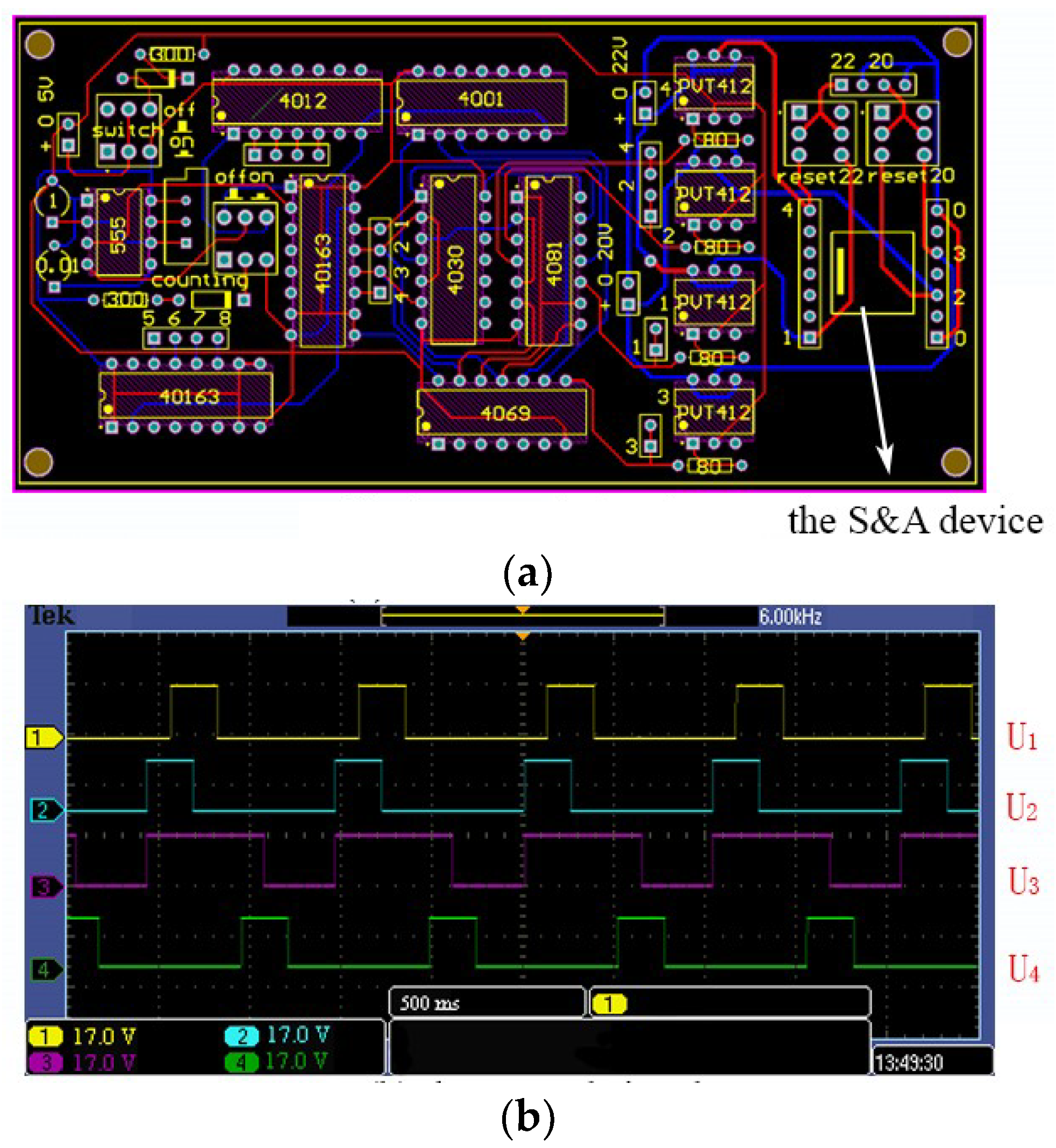
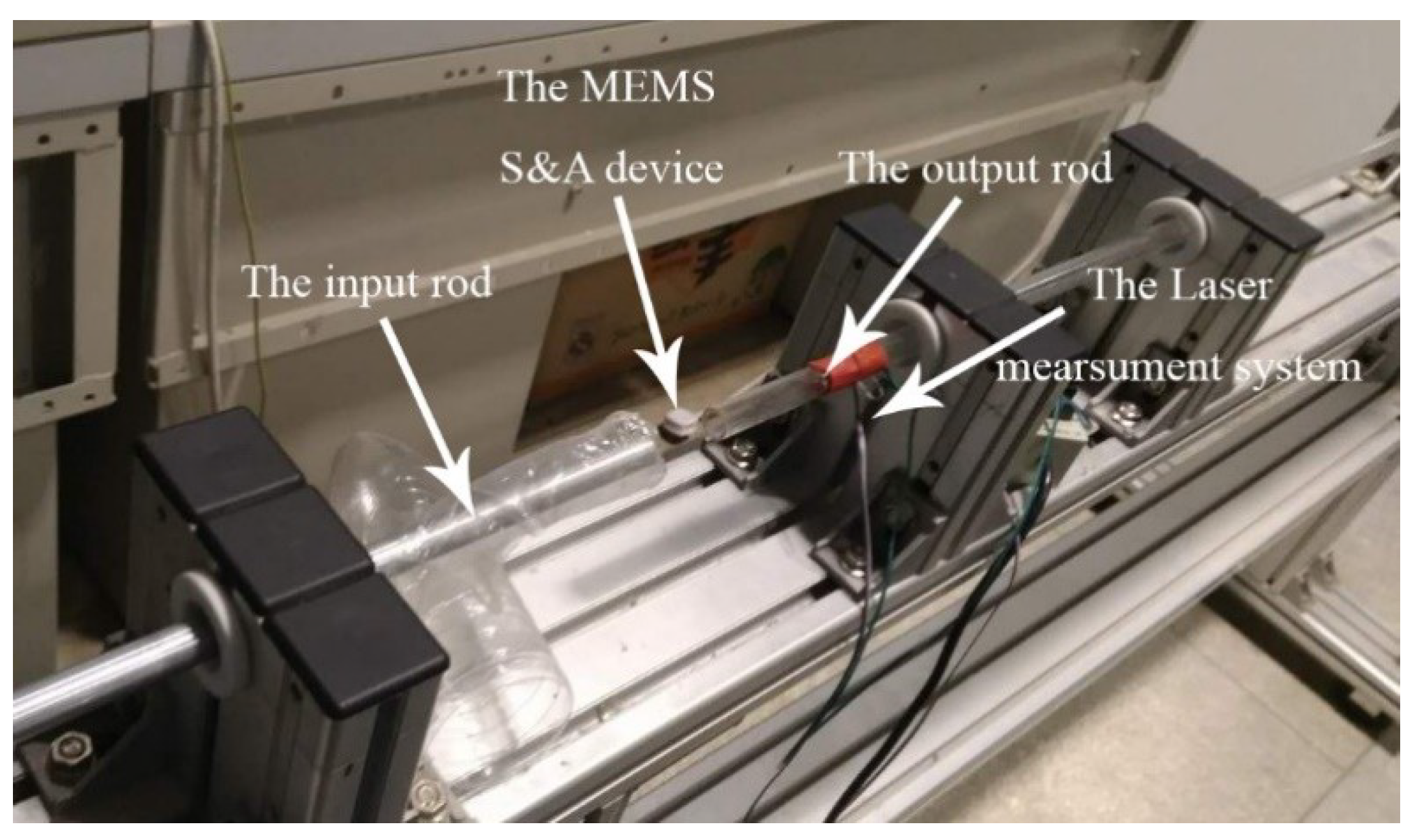
4. Tests of Actuation Performance
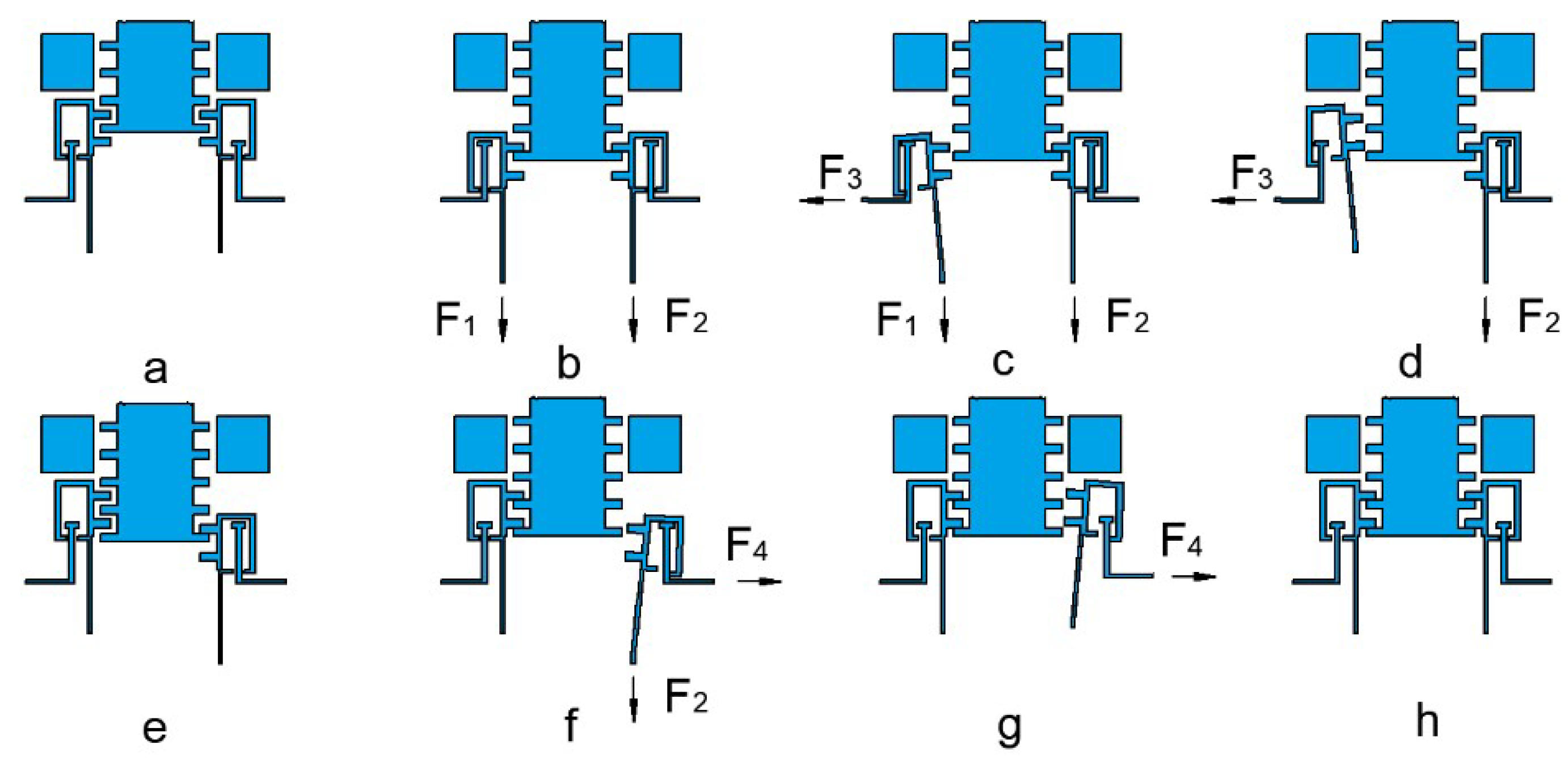
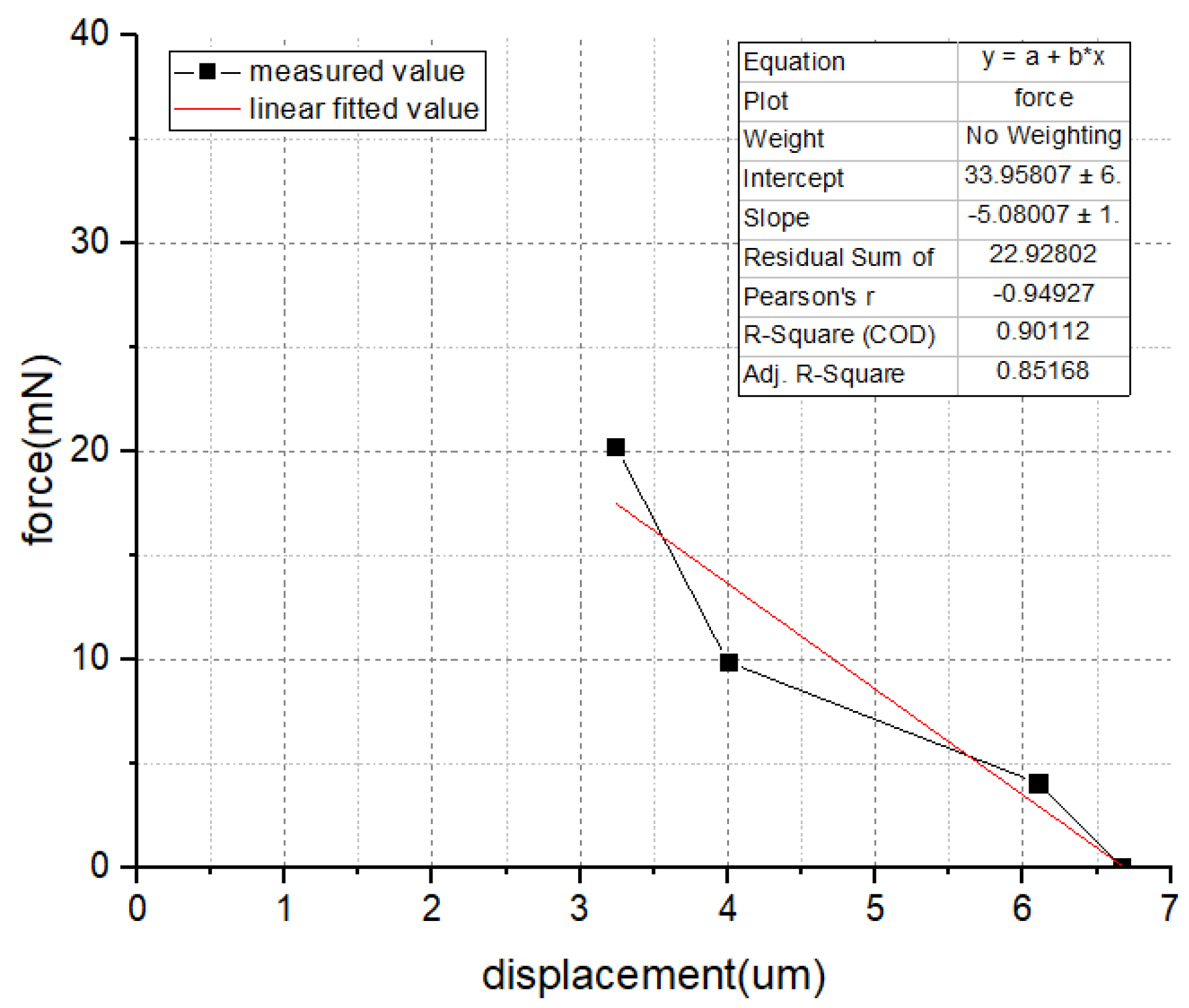
4.1. The Actuation Froce
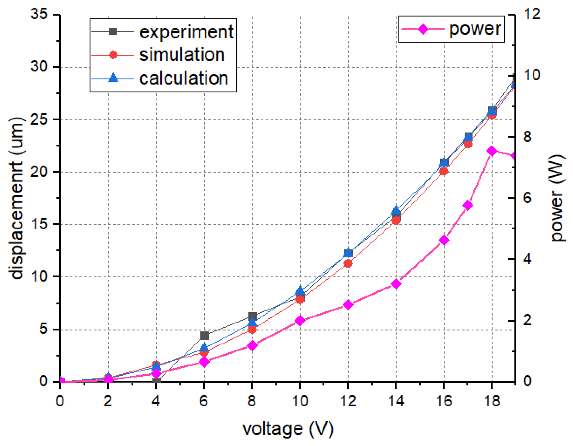
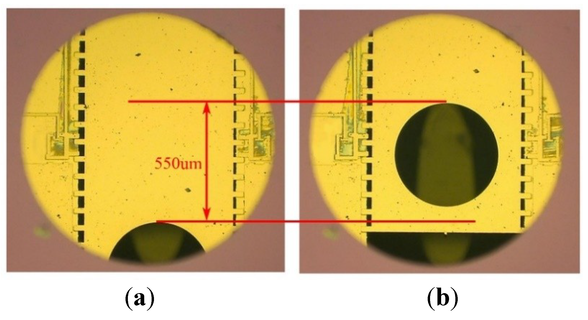
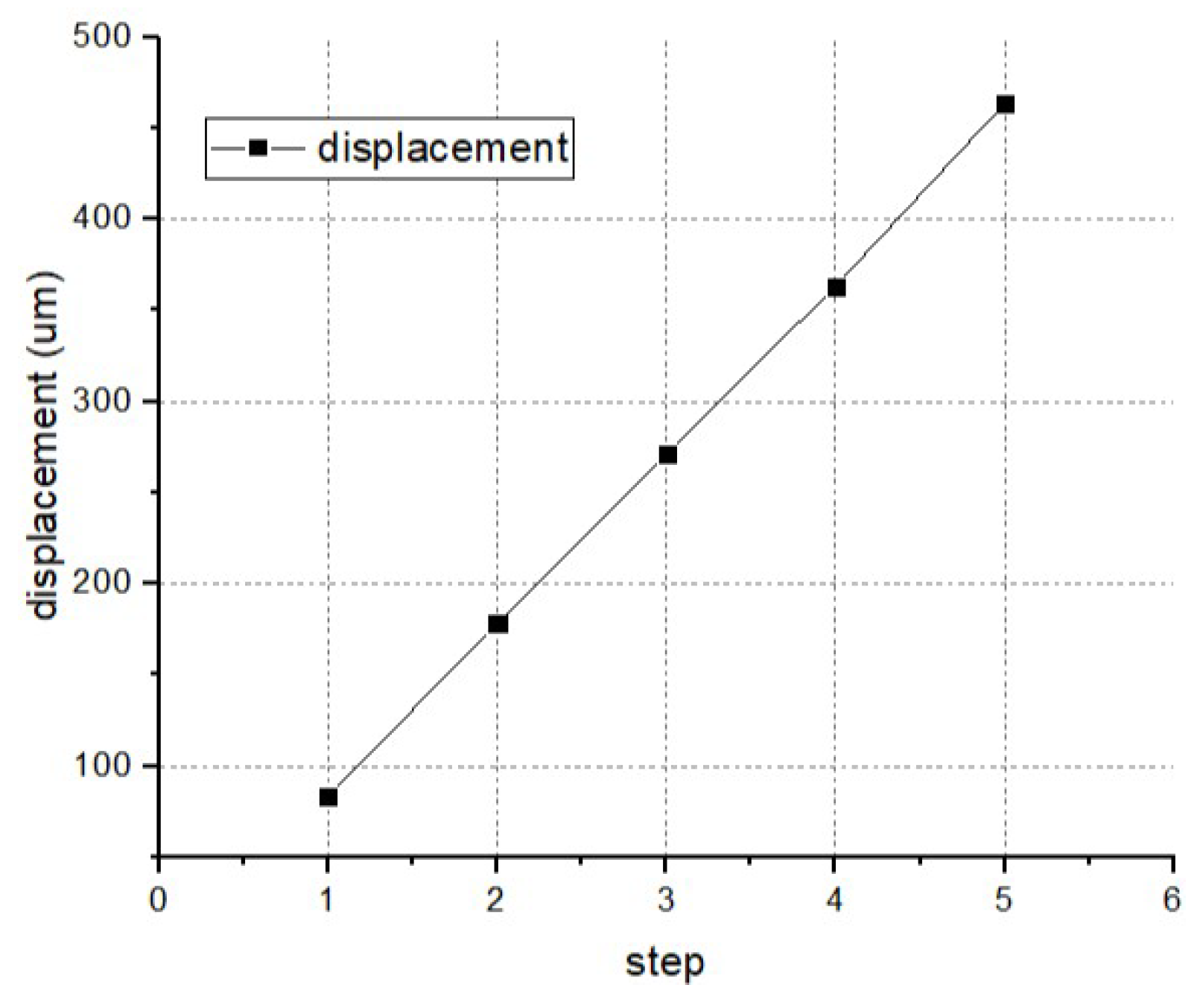
4.2. The Displacement of V-shape Actuator
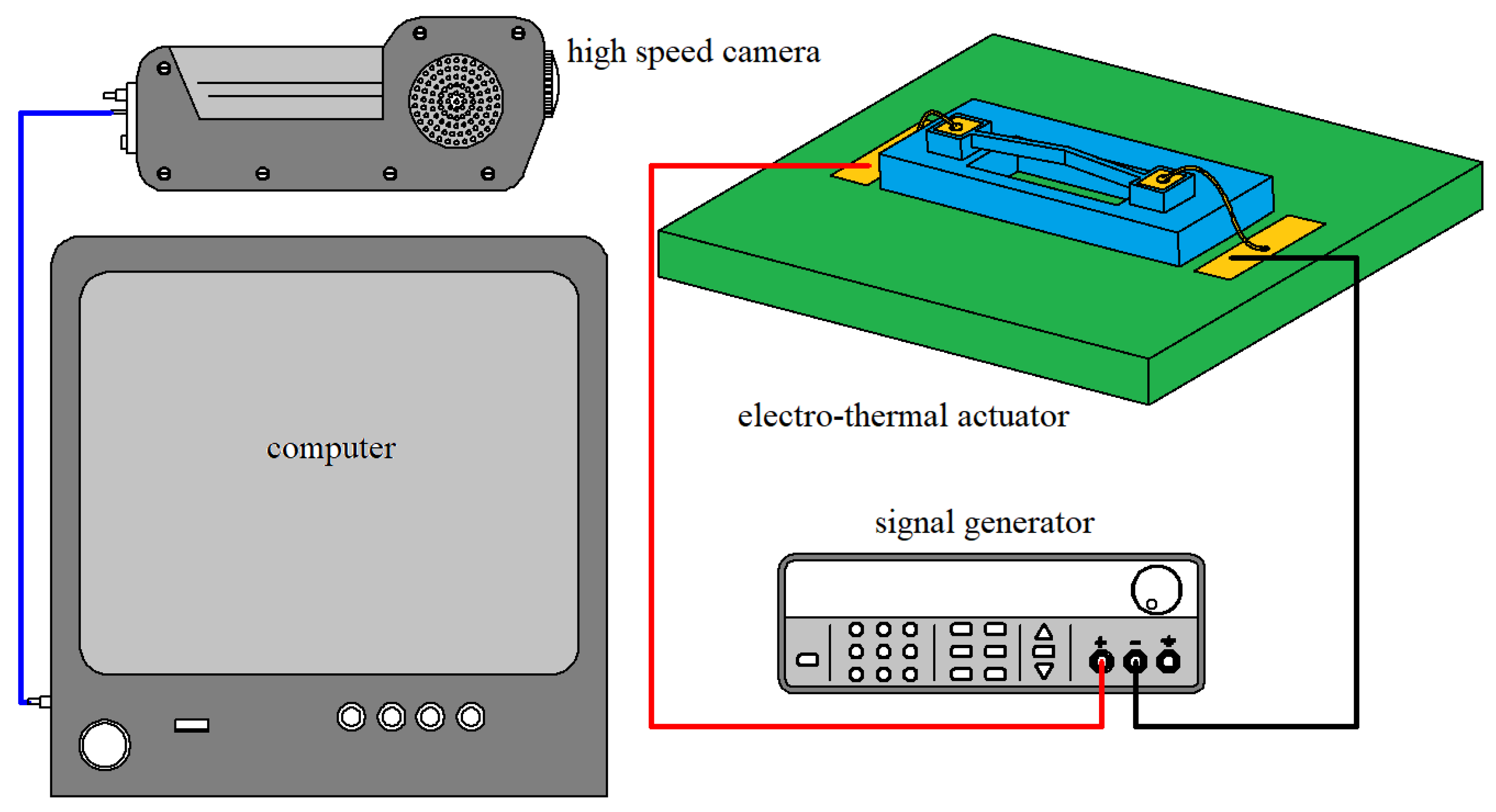
4.3. The Response Time
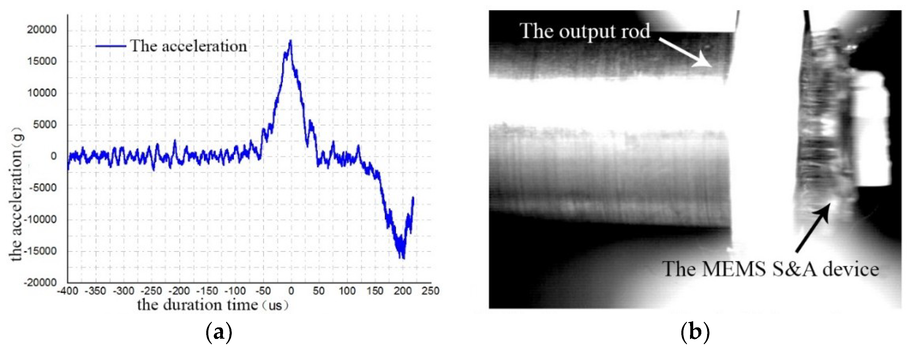
4.4. The Moving Tests
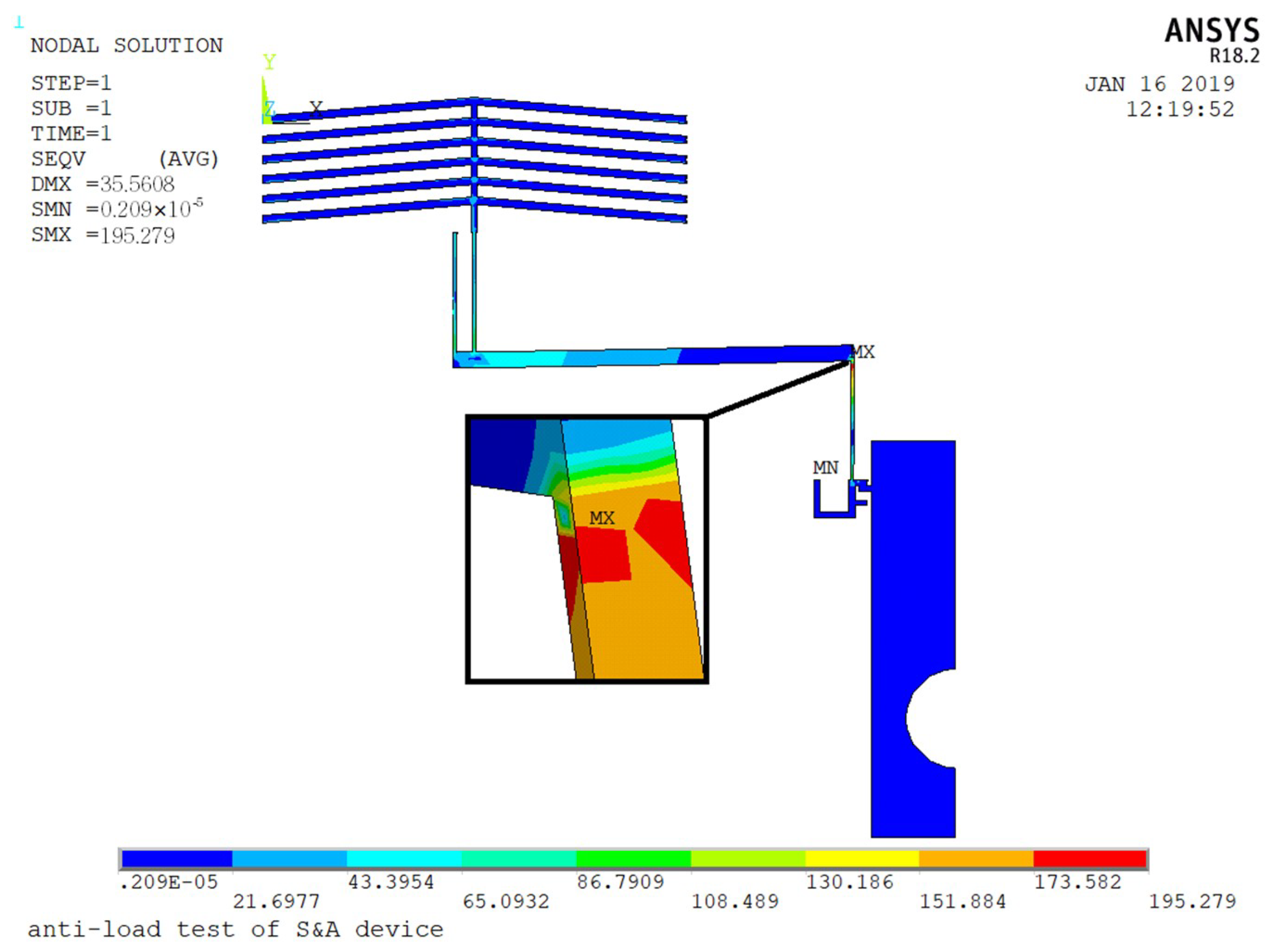
4.5. The Anti-Load Tests
5. Discussions and Conclusions
Author Contributions
Funding
Conflicts of Interest
References
- Zhang, J.; Li, D. Failure analysis of set-back arming process of MEMS S&A device. Sens. Transducers 2014, 166, 66–72. [Google Scholar]
- Li, X.; Zhao, Y.; Hu, T.; Xu, W.; Zhao, Y.; Bai, Y.; Ren, W. Design of a large displacement thermal actuator with a cascaded V-beam amplification for MEMS safety-and-arming devices. Microsystem Technologies 2015, 21, 2367–2374. [Google Scholar] [CrossRef]
- Robinson, C.H.; Wood, R.H.; Hoang, T.Q. Miniature MEMS-based electromechanical safety and arming device. U.S. Patent Number 6964231, 15 November 2005. [Google Scholar]
- Maurer, W.H.; Soto, G.H.; Hollingsworth, D.R. Method for utilizing a MEMS safe arm device for microdetonation. U.S. Patent Number 7007606, 7 March 2006. [Google Scholar]
- Jeong, J.-H.; Eom, J.; Lee, S.S.; Lim, D.W.; Jang, Y.I.; Seo, K.W.; Choi, S.S.; Lee, C.J.; Oh, J.S. Miniature mechanical safety and arming device with runaway escapement arming delay mechanism for artillery fuze. Sen. Actuators A 2018, 279, 518–524. [Google Scholar] [CrossRef]
- Wang, D.; Lou, W.; Feng, Y.; Zhang, X. Design of High-Reliability Micro Safety and Arming Devices for a Small Caliber Projectile. Micromachines 2017, 8, 234. [Google Scholar] [CrossRef] [PubMed]
- Bao, B.; Yan, N.; Geng, W.; Li, C. Simulation and experiment investigation on structural design and reinforcement of pyrotechnical sliding micro-actuators. Analog Integr. Circ. Signal Process. 2016, 3, 1–11. [Google Scholar] [CrossRef]
- Pezous, H.; Rossi, C.; Sanchez, M.; Mathieu, F.; Dollat, X.; Charlot, S.; Salvagnac, L.; Conédéra, V. Integration of a MEMS based safe arm and fire device. Sens. Actuators A 2010, 159, 157–167. [Google Scholar] [CrossRef]
- Preetham, B.S.; Mangels, J.A. Performance evaluation of a curved electrode actuator fabricated without gold/chromium conductive layers. Microsyst. Technol. Suppl. C 2018, 24, 3479–3485. [Google Scholar]
- Preetham, B.S.; Lake, M.A.; Hoelzle, D.J. A curved electrode electrostatic actuator designed for large displacement and force in an underwater environment. J. Micromech. Microeng. 2017, 27, 095009. [Google Scholar] [CrossRef]
- Hu, T.; Zhao, Y.; Zhao, Y.; Ren, W. Integration design of a MEMS based fuze. Sens. Actuators A 2017, 268, 193–200. [Google Scholar] [CrossRef]
- Hu, T.; Zhao, Y.; Li, X.; Zhao, Y.; Bai, Y. Integration design of MEMS electro-thermal safety-and-arming devices. Microsyst. Technol. 2016, 1–6. [Google Scholar] [CrossRef]
- Mink, S.S. Microelectromechanical System (MEMS) Interrupter for Safe and Arm Devices. Master’s Dissertation, Air Force Institute of Technology, Wright-Patterson AFB, OH, USA, 2006. [Google Scholar]
- Lake, R.A.; Starman, L.V.A.; Coutu, R.A. Electrothermal Actuators for Integrated MEMS Safe and Arming Devices. In Proceedings of the SEM Annual Conference, Indianapolis, IN, USA, 7–10 June 2010. [Google Scholar]
- Hu, T.; Zhao, Y.; Li, X.; Zhao, Y.; Bai, Y. Design and characterization of a microelectromechanical system electro-thermal linear motor with interlock mechanism for micro manipulators. Rev. Sci. Instrum. 2016, 87, 246. [Google Scholar] [CrossRef] [PubMed]
- Hickey, R.; Sameoto, D.; Hubbard, T.; Kujath, M. Time and frequency response of two-arm micromachined thermal actuators. J. Micromech. Microeng. 2003, 13, 40–46. [Google Scholar] [CrossRef]
- Zhang, Y.; Huang, Q.A.; Li, R.G.; Li, W. Macro-modeling for polysilicon cascaded bent beam electrothermal microactuators. Sens. Actuators A 2006, 128, 165–175. [Google Scholar] [CrossRef]
- Eniko, E.T.; Shantanu, S.S.; Lazarov, K.V. Analytical Model for Analysis and Design of V-Shaped Thermal Microactuators. J. Microelectromech. Syst. 2005, 14, 788–798. [Google Scholar] [CrossRef]
- Yang, Y.S.; Lin, Y.H.; Hu, Y.C.; Liu, C.-H. A large-displacement thermal actuator designed for MEMS pitch-tunable grating. J. Micromech. Microeng. 2009, 19, 15001–15012. [Google Scholar] [CrossRef]


| Parameters | Set1 Infeasible | Set2 Feasible | Set3 Feasible | Set4 Feasible | Set5 Feasible | Set6 Feasible | Set7 Feasible | *Set8* Feasible |
|---|---|---|---|---|---|---|---|---|
| Smax (MPa) | 617.05 | 638.20 | 645.39 | 644.27 | 638.55 | 638.21 | 620.59 | 636.84 |
| Dmax (μm) | 183.85 | 257.85 | 235.52 | 243.16 | 227.62 | 224.62 | 223.90 | 223.70 |
| L (μm) | 1600 | 2338.8 | 2155.2 | 2215 | 2044.8 | 2011.6 | 2003.8 | 2001.6 |
| w (μm) | 20 | 34.572 | 36.924 | 36.179 | 31.403 | 30.341 | 30.103 | 30.037 |
| Volume (μm3) | 0.1887 × 10⁸ | 0.33468 × 10⁸ | 0.33054 × 10⁸ | 0.33232 × 10⁸ | 0.28478 × 10⁸ | 0.27531 × 10⁸ | 0.27318 × 10⁸ | 0.27259 × 10⁸ |
| The Cover Plate (Silicon Wafer) | The Actuation Chip (SOI Wafer) | The Barrel Plate (Silicon Wafer) | ||||
|---|---|---|---|---|---|---|
| Parameters | Specification | Parameters | Specification | Parameters | Specification | |
| Diameter (mm) | 100 | Diameter (mm) | 100 | Diameter (mm) | 100 | |
| Orientation | (100) | Orientation | (100) | Orientation | (100) | |
| Resistivity (Ω∙cm) | 1–20 | Resistivity (Ω∙cm) | Device layer | 0.01–0.02 | Resistivity (Ω∙cm) | 1–20 |
| Handle layer | 1–20 | |||||
| Thickness (μm) | 300 | Thickness (μm) | Device layer | 50 | Thickness (μm) | 500 |
| Buried oxide layer | 3 | |||||
| Handle layer | 400 | |||||
| Step (Decimalism) | Step (Binary) | U1 | U2 | U3 | U4 | ||
|---|---|---|---|---|---|---|---|
| N | C | B | A | ||||
| 0 | 0 | 0 | 0 | 0 | 0 | 0 | 0 |
| 1 | 0 | 0 | 1 | 0 | 1 | 1 | 0 |
| 2 | 0 | 1 | 0 | 1 | 1 | 1 | 0 |
| 3 | 0 | 1 | 1 | 1 | 0 | 1 | 0 |
| 4 | 1 | 0 | 0 | 0 | 0 | 1 | 0 |
| 5 | 1 | 0 | 1 | 0 | 0 | 1 | 1 |
| 6 | 1 | 1 | 0 | 0 | 0 | 0 | 1 |
| 7 | 1 | 1 | 1 | 0 | 0 | 0 | 0 |
© 2019 by the authors. Licensee MDPI, Basel, Switzerland. This article is an open access article distributed under the terms and conditions of the Creative Commons Attribution (CC BY) license (http://creativecommons.org/licenses/by/4.0/).
Share and Cite
Hu, T.; Ren, W.; Zhao, Y.; Xue, Y. The Research on Actuation Performance of MEMS Safety-and-Arming Device with Interlock Mechanism. Micromachines 2019, 10, 76. https://doi.org/10.3390/mi10020076
Hu T, Ren W, Zhao Y, Xue Y. The Research on Actuation Performance of MEMS Safety-and-Arming Device with Interlock Mechanism. Micromachines. 2019; 10(2):76. https://doi.org/10.3390/mi10020076
Chicago/Turabian StyleHu, Tengjiang, Wei Ren, Yulong Zhao, and Yan Xue. 2019. "The Research on Actuation Performance of MEMS Safety-and-Arming Device with Interlock Mechanism" Micromachines 10, no. 2: 76. https://doi.org/10.3390/mi10020076
APA StyleHu, T., Ren, W., Zhao, Y., & Xue, Y. (2019). The Research on Actuation Performance of MEMS Safety-and-Arming Device with Interlock Mechanism. Micromachines, 10(2), 76. https://doi.org/10.3390/mi10020076