Slot-Die Coating of Double Polymer Layers for the Fabrication of Organic Light Emitting Diodes


Abstract
1. Introduction
2. Materials and Methods
2.1. Materials
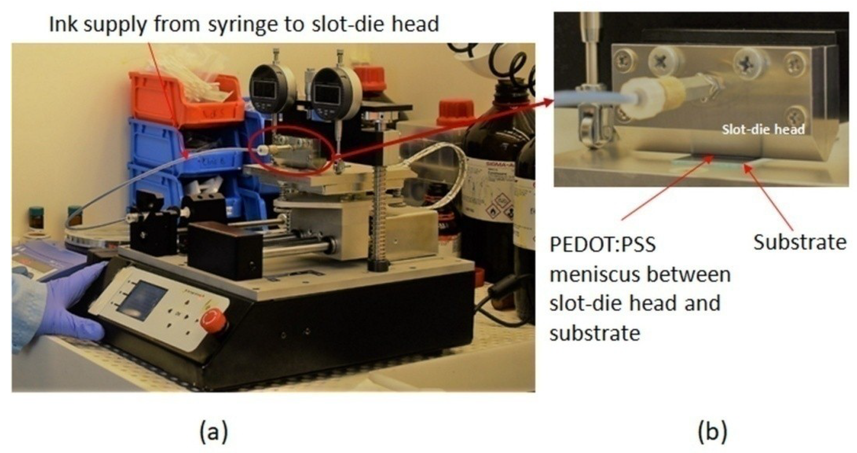
2.2. Instruments
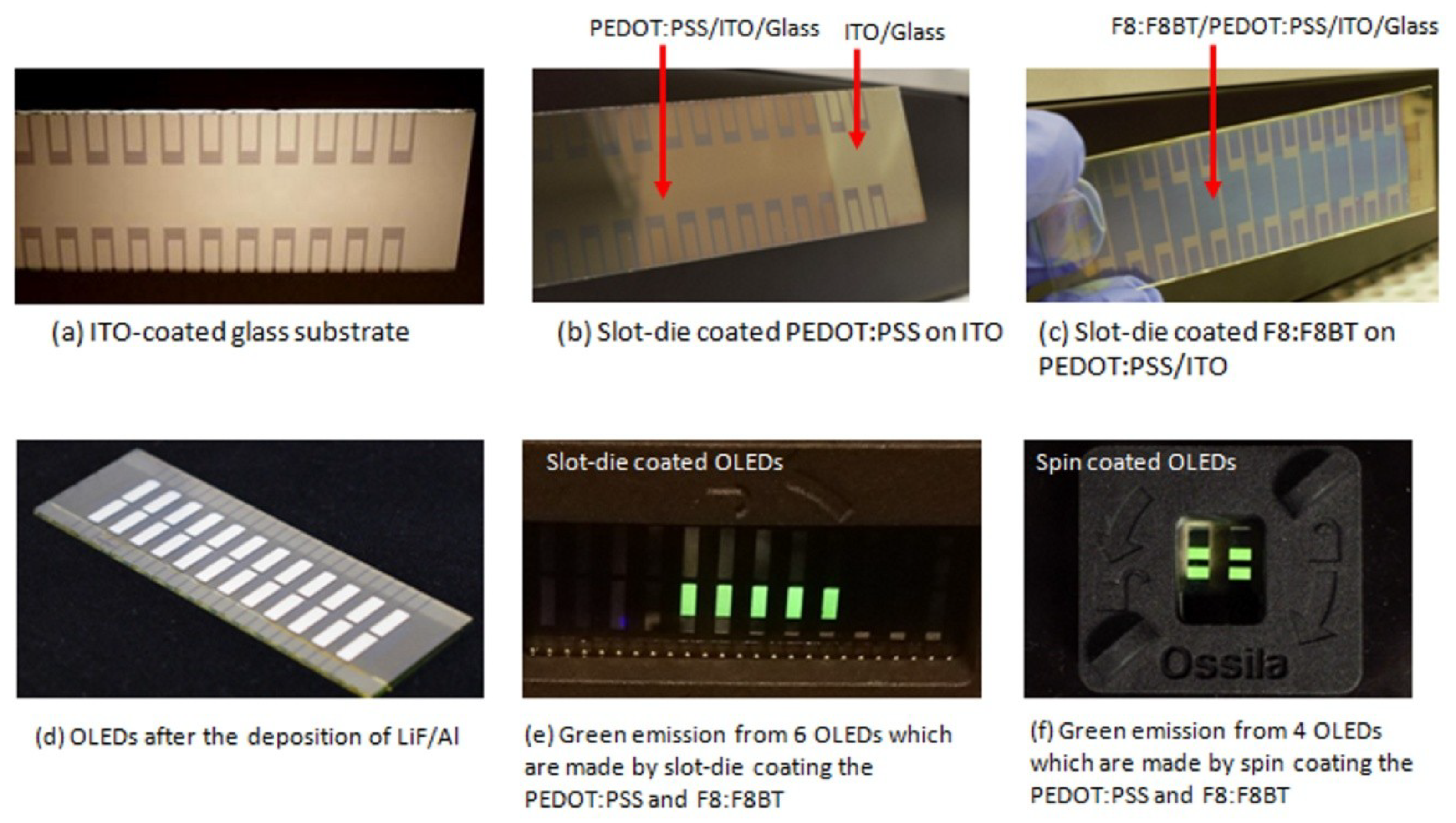
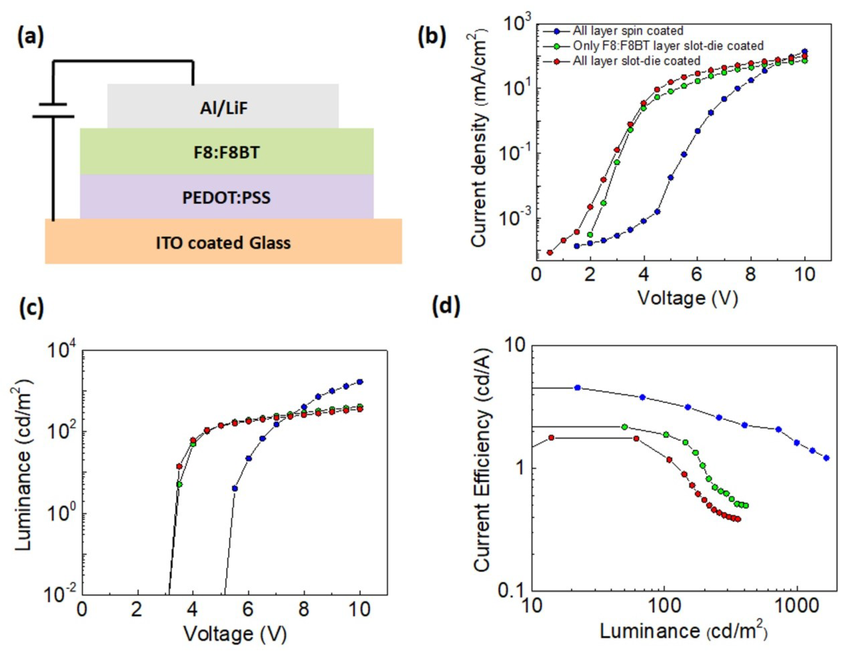
2.3. Fabrication of OLEDs
3. Results and Discussions
3.1. Optimization of PEDOT:PSS Slot-Die Coating
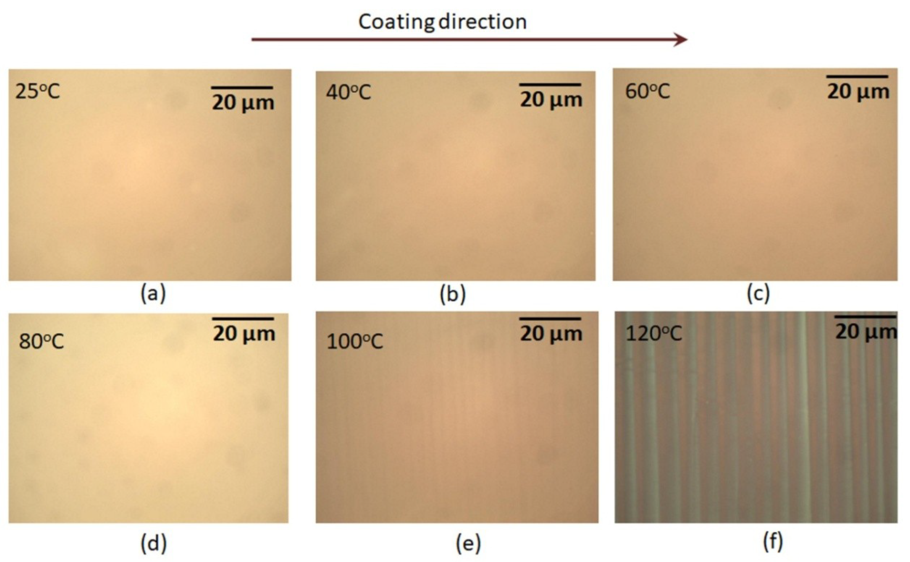
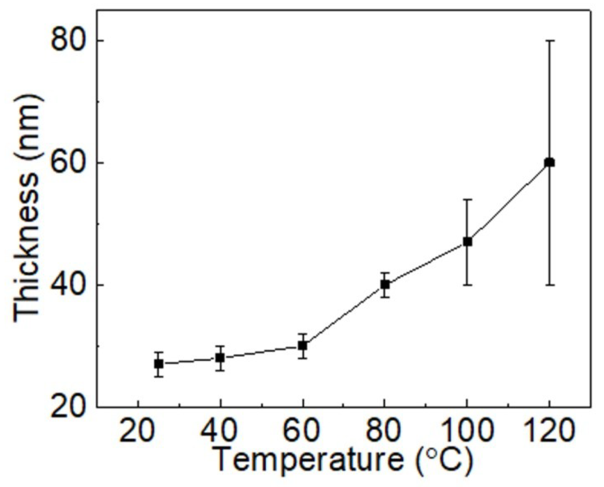
3.1.1. Influence of Substrate Temperature
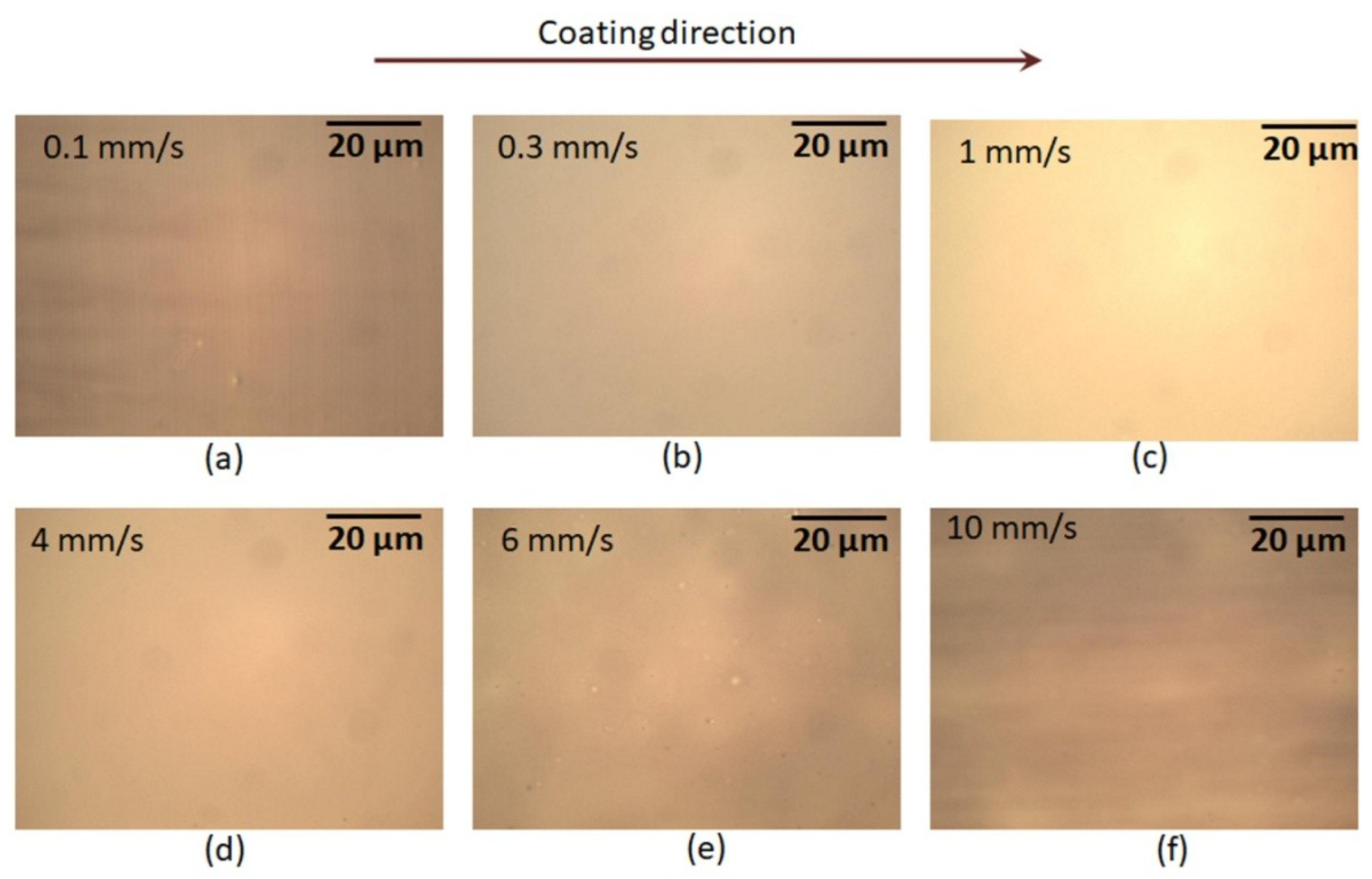
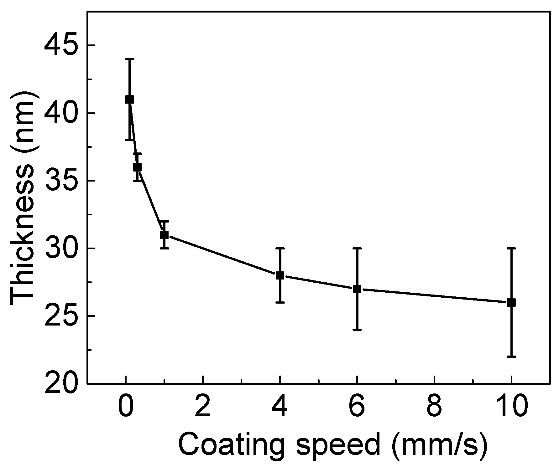
3.1.2. Influence of Slot-Die Coating Speed
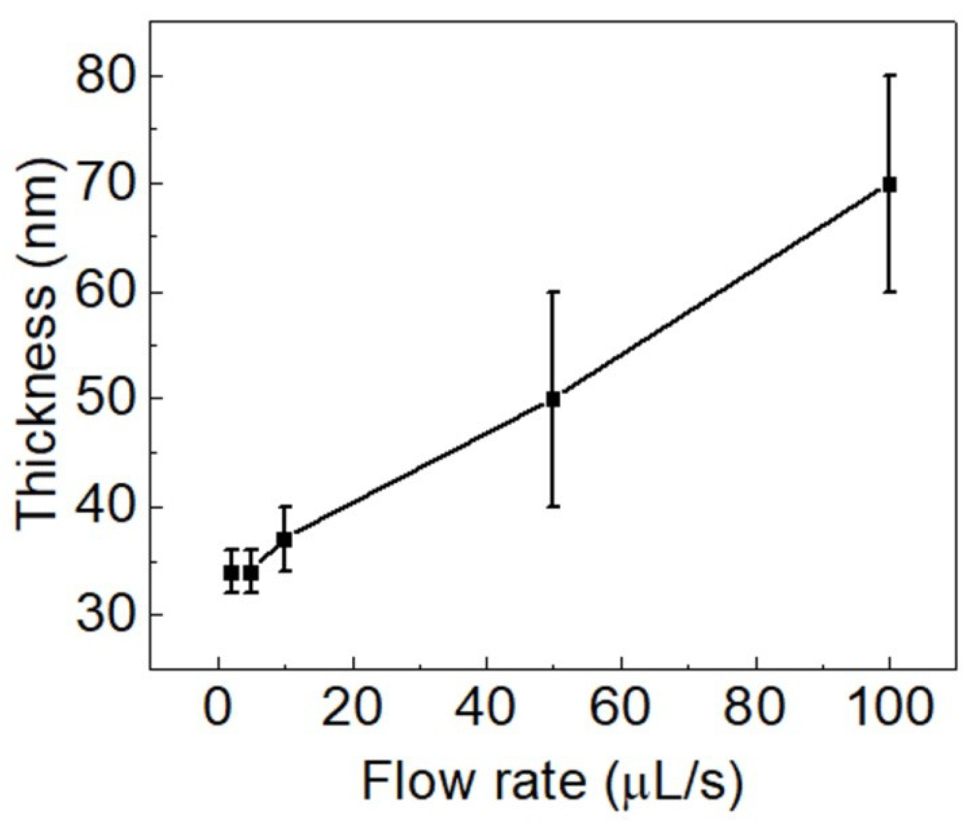
3.1.3. Influence of Ink Flow Rate
3.2. Slot-Die Coating of F8:F8BT Film
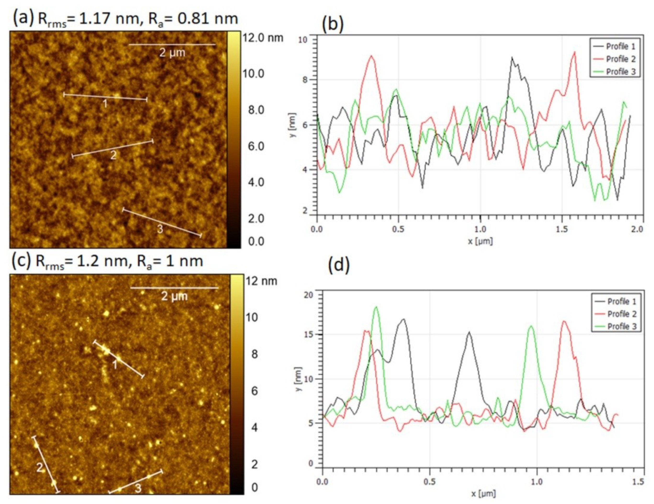
3.3. AFM Images of Slot-Die Coated PEDOT:PSS and F8:F8BT Films
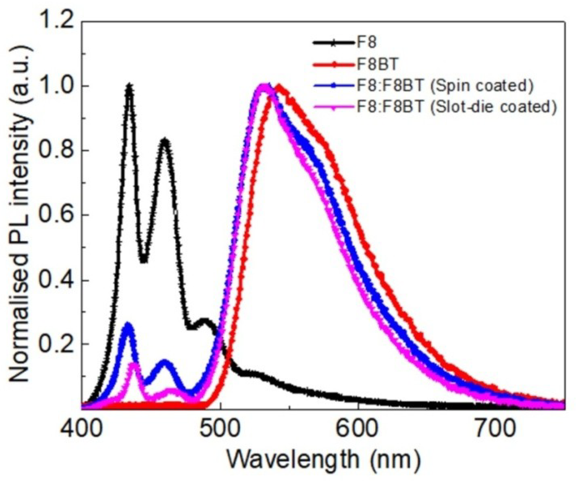
3.4. Photoluminescence (PL) Measurements
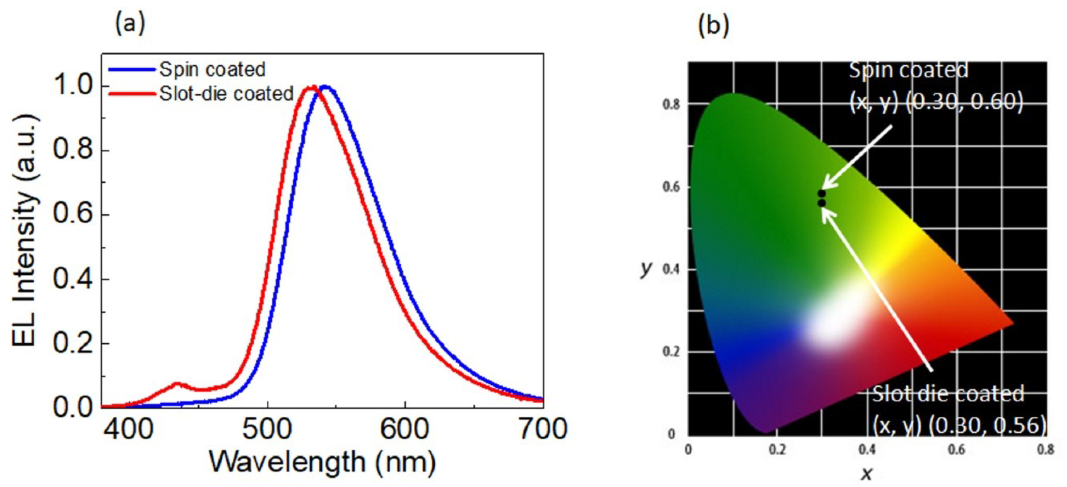
3.5. Performances of Slot-Die Coated OLEDs
4. Conclusions
Author Contributions
Funding
Conflicts of Interest
References
- Riegel, A.-L.; Reichelt, N.; Scharfer, P.; Schabel, W. Process-dependent conductivity and film homogeneity of slot-die-coated PEDOT:PSS–PVA composite films. J. Coat. Technol. Res. 2017, 14, 1039–1051. [Google Scholar] [CrossRef]
- Raupp, S.M.; Merklein, L.; Hietzschold, S.; Zürn, M.; Scharfer, P.; Schabel, W. Slot die-coated blue SMOLED multilayers. J. Coat. Technol. Res. 2017, 14, 1029–1037. [Google Scholar] [CrossRef]
- Carey, T.; Cacovich, S.; Divitini, G.; Ren, J.; Mansouri, A.; Kim, J.M.; Wang, C.; Ducati, C.; Sordan, R.; Torrisi, F. Fully inkjet-printed two-dimensional material field-effect heterojunctions for wearable and textile electronics. Nat. Commun. 2017, 8, 1202. [Google Scholar] [CrossRef] [PubMed]
- Ostfeld, A.E.; Deckman, I.; Gaikwad, A.M.; Lochner, C.M.; Arias, A.C. Screen printed passive components for flexible power electronics. Sci. Rep. 2015, 5, 15959. [Google Scholar] [CrossRef] [PubMed]
- Lewis, J.A.; Ahn, B.Y. Device fabrication: Three-dimensional printed electronics. Nature 2015, 518, 42–43. [Google Scholar] [CrossRef] [PubMed]
- C, A.; Luszczynska, B.; Dupont, B.G.R.; Sieradzki, Z. Inkjet Printing Technique and Its Application in Organic Light Emitting Diodes. Disp. Imaging 2017, 2, 339–358. [Google Scholar]
- Hoeng, F.; Denneulin, A.; Bras, J. Use of nanocellulose in printed electronics: A review. Nanoscale 2016, 8, 13131–13154. [Google Scholar] [CrossRef]
- Sarma, K. Recent progress in OLED and flexible displays and their potential for application to aerospace and military display systems. In Proceedings of the SPIE Defense + Security, Baltimore, MD, USA, 20–24 April 2015; p. 11. [Google Scholar]
- Alonso-Lomillo, M.A.; Dominguez-Renedo, O.; Arcos-Martinez, M.J. Screen-printed biosensors in microbiology; a review. Talanta 2010, 82, 1629–1636. [Google Scholar] [CrossRef]
- Shin, D.; Lee, J.-Y.; Hong, K.-Y.; Park, J.; Seo, Y.-S. Slot-die coating of organic thin films for active-matrix organic light-emitting diode displays. Thin Solid Film 2016, 619, 179–186. [Google Scholar] [CrossRef]
- Pérez-Gutiérrez, E.; Lozano, J.; Gaspar-Tánori, J.; Maldonado, J.-L.; Gómez, B.; López, L.; Amores-Tapia, L.-F.; Barbosa-García, O.; Percino, M.-J. Organic solar cells all made by blade and slot–die coating techniques. Sol. Energy 2017, 146, 79–84. [Google Scholar] [CrossRef]
- Lin, Z.; Guo, X.; Zhou, L.; Zhang, C.; Chang, J.; Wu, J.; Zhang, J. Solution-processed high performance organic thin film transistors enabled by roll-to-roll slot die coating technique. Org. Electron. 2018, 54, 80–88. [Google Scholar] [CrossRef]
- Lee, H.; Lee, D.; Hwang, J.; Nam, D.; Byeon, C.; Ko, S.H.; Lee, S. Silver nanoparticle piezoresistive sensors fabricated by roll-to-roll slot-die coating and laser direct writing. Opt. Express 2014, 22, 8919–8927. [Google Scholar] [CrossRef] [PubMed]
- Huang, Y.; Cha, H.; Chen, C.; Tsao, C. A universal roll-to-roll slot-die coating approach towards high-efficiency organic photovoltaics. Prog. Photovolt. Res. Appl. 2017, 25, 928–935. [Google Scholar] [CrossRef]
- Abbel, R.; de Vries, I.; Langen, A.; Kirchner, G.; t’Mannetje, H.; Gorter, H.; Wilson, J.; Groen, P. Toward high volume solution based roll-to-roll processing of OLEDs. J. Mater. Res. 2017, 32, 2219–2229. [Google Scholar] [CrossRef]
- Peters, K.; Raupp, S.; Hummel, H.; Bruns, M.; Scharfer, P.; Schabel, W. Formation of blade and slot die coated small molecule multilayers for OLED applications studied theoretically and by XPS depth profiling. AIP Adv. 2016, 6, 065108. [Google Scholar] [CrossRef]
- Mattias, A.L. Fully Slot–Die-Coated All-Organic Solar Cells. Energy Technol. 2015, 3, 437–442. [Google Scholar] [CrossRef]
- Sandström, A.; Dam, H.F.; Krebs, F.C.; Edman, L. Ambient fabrication of flexible and large-area organic light-emitting devices using slot-die coating. Nat. Commun. 2012, 3, 1002. [Google Scholar] [CrossRef]
- Volz, D.; Wallesch, M.; Flechon, C.; Danz, M.; Verma, A.; Navarro, J.M.; Zink, D.M.; Brase, S.; Baumann, T. From iridium and platinum to copper and carbon: New avenues for more sustainability in organic light-emitting diodes. Green Chem. 2015, 17, 1988–2011. [Google Scholar] [CrossRef]
- Wolfgang, B.; Jörg, F.; Tobias, D.S.; Bert, J.S.; Christian, M. Device efficiency of organic light-emitting diodes: Progress by improved light outcoupling. Phys. Status Solidi A 2013, 210, 44–65. [Google Scholar] [CrossRef]
- Thejo Kalyani, N.; Dhoble, S.J. Organic light emitting diodes: Energy saving lighting technology—A review. Renew. Sustain. Energy Rev. 2012, 16, 2696–2723. [Google Scholar] [CrossRef]
- Chizu, S.; Yoshiaki, T.; Takeshi, Y.; Makoto, K.; Shuji, D. Recent progress of high performance polymer OLED and OPV materials for organic printed electronics. Sci. Technol. Adv. Mater. 2014, 15, 034203. [Google Scholar]
- Lövenich, W. PEDOT-properties and applications. Polym. Sci. Ser. C 2014, 56, 135–143. [Google Scholar] [CrossRef]
- Yu, D.X. Light-emitting devices with conjugated polymers. Int. J. Mol. Sci. 2011, 12, 1575–1594. [Google Scholar] [CrossRef] [PubMed]
- Alsalhi, M.S.; Alam, J.; Dass, L.A.; Raja, M. Recent advances in conjugated polymers for light emitting devices. Int. J. Mol. Sci. 2011, 12, 2036–2054. [Google Scholar] [CrossRef] [PubMed]
- Morgado, J.; Moons, E.; Friend, R.H.; Cacialli, F. De-mixing of Polyfluorene-Based Blends by Contact with Acetone: Electro- and Photo-luminescence Probes. Adv. Mater. 2001, 13, 810–814. [Google Scholar] [CrossRef]
- Wilkinson, C.I.; Lidzey, D.G.; Palilis, L.C.; Fletcher, R.B.; Martin, S.J.; Wang, X.H.; Bradley, D.D.C. Enhanced performance of pulse driven small area polyfluorene light emitting diodes. Appl. Phys. Lett. 2001, 79, 171–173. [Google Scholar] [CrossRef]
- Morgado, J.; Friend, R.H.; Cacialli, F. Improved efficiency of light-emitting diodes based on polyfluorene blends upon insertion of a poly(p-phenylene vinylene) electron- confinement layer. Appl. Phys. Lett. 2002, 80, 2436–2438. [Google Scholar] [CrossRef]
- Wei, B.; Ichikawa, M.; Furukawa, K.; Koyama, T.; Taniguchi, Y. High peak luminance of molecularly dye-doped organic light-emitting diodes under intense voltage pulses. J. Appl. Phys. 2005, 98, 044506. [Google Scholar] [CrossRef]
- Zhang, Y.; Blom, P.W.M. Electron and hole transport in poly(fluorene-benzothiadiazole). Appl. Phys. Lett. 2011, 98, 143504. [Google Scholar] [CrossRef]
- Suh, M.; Bailey, J.; Kim, S.W.; Kim, K.; Yun, D.-J.; Jung, Y.; Hamilton, I.; Chander, N.; Wang, X.; Bradley, D.D.C.; et al. High-Efficiency Polymer LEDs with Fast Response Times Fabricated via Selection of Electron-Injecting Conjugated Polyelectrolyte Backbone Structure. ACS Appl. Mater. Interfaces 2015, 7, 26566–26571. [Google Scholar] [CrossRef]
- Hill, J.; Heriot, S.Y.; Worsfold, O.; Richardson, T.H.; Fox, A.M.; Bradley, D.D.C. Dynamics of Förster transfer in polyfluorene-based polymer blends and Langmuir–Blodgett nanostructures. Synth. Met. 2003, 139, 787–790. [Google Scholar] [CrossRef]
- Jokinen, K.; Bykov, A.V.; Sliz, R.; Remes, K.; Fabritius, T.; Myllylä, R. Light Emission Color Conversion of Polyfluorene-Blend OLEDs Induced by Thermal Annealing. IEEE Trans. Electron Devices 2015, 62, 2238–2243. [Google Scholar] [CrossRef]
- Voigt, M.; Chappell, J.; Rowson, T.; Cadby, A.; Geoghegan, M.; Jones, R.A.L.; Lidzey, D.G. The interplay between the optical and electronic properties of light-emitting-diode applicable conjugated polymer blends and their phase-separated morphology. Org. Electron. 2005, 6, 35–45. [Google Scholar] [CrossRef]
- Chuan, L.; Yong, X.; Xuying, L.; Takeo, M.; Henning, S.; Yong-Young, N. Solution-processed high-LUMO-level polymers in n -type organic field-effect transistors: A comparative study as a semiconducting layer, dielectric layer, or charge injection layer. Semicond. Sci. Technol. 2015, 30, 044007. [Google Scholar]
- Hirotake, K.; Takahiro, O.; Yutaka, O. Electroluminescence emission patterns of organic light-emitting transistors based on crystallized fluorene-type polymers. Jpn. J. Appl. Phys. 2017, 56, 03BA01. [Google Scholar]
- Raupp, S.M.; Merklein, L.; Pathak, M.; Scharfer, P.; Schabel, W. An experimental study on the reproducibility of different multilayer OLED materials processed by slot die coating. Chem. Eng. Sci. 2017, 160, 113–120. [Google Scholar] [CrossRef]


| Slot-Die Coated Films | Substrate Temperature (°C) | Coating Speed (mm/s) | Flow Rate of Ink (μL/s) |
|---|---|---|---|
| PEDOT:PSS | 60 | 0.5 | 1 |
| F8:F8BT | 35 | 0.3 | 1 |
| OLEDs Using Slot-Die Coating and/or Spin Coating Technique | PEDOT:PSS Thickness (nm) | F8:F8BT Thickness (nm) | Turn-on Voltage (V) | Luminance (cd/m2) at 10 V | Max. Current Efficiency (cd/A) |
|---|---|---|---|---|---|
| Slot-Die Coated OLEDs | 34 ± 3 | 66 ± 5 | 3.5 | 357 | 1.77 |
| F8:F8BT Slot-Die Coated and PEDOT:PSS Spin Coated | 35 ± 1 | 66 ± 5 | 3.5 | 411 | 2.16 |
| Spin-Coated OLEDs | 35 ± 1 | 70 ± 1 | 5.5 | 1662 | 4.51 |
© 2019 by the authors. Licensee MDPI, Basel, Switzerland. This article is an open access article distributed under the terms and conditions of the Creative Commons Attribution (CC BY) license (http://creativecommons.org/licenses/by/4.0/).
Share and Cite
C, A.; Colella, M.; Griffin, J.; Kingsley, J.; Scarratt, N.; Luszczynska, B.; Ulanski, J. Slot-Die Coating of Double Polymer Layers for the Fabrication of Organic Light Emitting Diodes. Micromachines 2019, 10, 53. https://doi.org/10.3390/mi10010053
C A, Colella M, Griffin J, Kingsley J, Scarratt N, Luszczynska B, Ulanski J. Slot-Die Coating of Double Polymer Layers for the Fabrication of Organic Light Emitting Diodes. Micromachines. 2019; 10(1):53. https://doi.org/10.3390/mi10010053
Chicago/Turabian StyleC, Amruth, Marco Colella, Jonathan Griffin, James Kingsley, Nicholas Scarratt, Beata Luszczynska, and Jacek Ulanski. 2019. "Slot-Die Coating of Double Polymer Layers for the Fabrication of Organic Light Emitting Diodes" Micromachines 10, no. 1: 53. https://doi.org/10.3390/mi10010053
APA StyleC, A., Colella, M., Griffin, J., Kingsley, J., Scarratt, N., Luszczynska, B., & Ulanski, J. (2019). Slot-Die Coating of Double Polymer Layers for the Fabrication of Organic Light Emitting Diodes. Micromachines, 10(1), 53. https://doi.org/10.3390/mi10010053