1. Introduction
The progress made in micro- and nano-technology industry over the last six decades has relied heavily on thin film technology. The versatile process of thin film deposition, lithography and etching has provided society with powerful miniaturized computers, equipped with transducers, communication channels and storage capabilities. Nanotechnology will continue to provide us with more, more powerful and smaller systems, primarily because of the ever reducing size of components.
The continuing decrease in size inevitably leads to the emergence of fundamental limits. Since the tiniest units of information are found in non-volatile storage systems (such as the hard disk), the first encounter with those limits was found in that area, where it expressed itself in the thermal stability of written bits [
1]. Non-volatile data storage will therefore move away from magnetism, possibly in the direction of ferro-electrics [
2] or phase-change [
3]. Ultimately, we will store bits of information into single atoms [
4].
Thin film technology is inherently two-dimensional, so we are accustomed to measuring progress in the number of transistors or stored bits per unit area. From a user point of view however, only the number of elements per unit volume is of interest. It seems to be in place to design new strategies which continue on the path towards increasing volumetric, rather than surface, densities. Since the fundamental limits express themselves first in non-volatile storage, the first steps into the third dimension will be taken in this field.
The key idea in this paper is to machine suitable nano-particles and assemble them in a self-assembly process. Each nanoparticle will have the functionality to store one or more bits of information. When assembled in three-dimensional structures, the volumetric data density can grow far beyond the limit of two-dimensional storage.
By equipping particles with electronic functionality, we open the route towards three dimensional processors. On the long term, we can envision mixtures of particles with embedded digital electronics, non-volatile memory and communication circuits, combined in cubic millimeter computers.
In this paper we will limit ourselves to non-volatile data storage however. We will discuss the data storage roadmap and estimate when limits will be reached in
Section 2, where we argue that solutions based on today’s three-dimensional storage systems are not capable to meet the density or price requirements. Addressing will be discussed in
Section 3, where it is shown that a three plane addressing scheme is to be preferred for large arrays. Subsequently we give two examples, based on transistors with memory elements (
Section 4) and magnetic ring cores (
Section 5). Realisation of this three-dimensional non-volatile memory will depend on our ability to steer self-assembly of nano-particles, which will be shortly discussed in
Section 6. Finally, we demonstrate in
Section 7 how an actual three-dimensional ring-core memory can be assembled from a limited number of tetragonal unit cells.
2. The Challenge in Non-Volatile Data Storage
The world of non-volatile data storage can be divided into two realms. On one side we have mechanically addressed memories, where information is addressed by physical movement of a read/write head. Famous examples are the record player, generations of optical storage media (from CD to Bluray disk), magnetic tape and hard-disks. Since the bit dimensions are determined by the size of one single—or only a few—read/write heads and by positioning accuracies, the data density of these media is generally very high. Mechanical addressing is however relatively slow (ms), and usually applied in situations where large amounts of data need to be stored which are not needed frequently. The highest data density is found in magnetic hard disk storage, and lies currently around 800 Gb/in
. The growth in hard disk data density fluctuates between 40% and 100% per year. Predictions are that magnetic storage is limited to data densities of about 10 Tb/in
[
5], which is another eight years from now at a growth rate of 40%. Probe storage technology [
6] offers the possibility to increase the data density all the way up to one bit per atom data storage [
4]. At this point the data density will be in the order of 250 Tb/in
, which will be in 2020 with an average growth rate of 60% per year. It is not clear however how areal data density will increase beyond this point.
On the other side, we have electrically addressed memories such as DRAM, FlashMemory, MRAM, Phase-Change RAM, etc. Since every bit is connected to the outside world by means of wiring, data rates and access times are high (ns). The capacity, or better bit density, of these media is limited by lithography, and follows the semiconductor industry roadmap. If the half-pitch linewidth is Λ, the minimum cell size is 4, and with multilevel storage at n bits per cell, the bit density becomes . The International Technology Roadmap for Semiconductors predicts that in 2020 Λ will be 11 nm (www.itrs.net). At a foreseen 4 bits per cell, the data density in electrically addressed storage will be 5 Tb/in. Consequently, electrically addressed memories will be far too expensive to take over the role of mechanically addressed memories in large capacity data storage systems in which access times of milliseconds are not an issue.
Areal data densities only give information about the relative cost of the system, but not about the final dimensions. From a user viewpoint, we are much more interested in capacity per unit volume. This is exactly the reason why tape recording systems are still persisting, even though their areal density is two orders of magnitude below the disk version of magnetic data storage. Assuming that in 2020 a probe recording system will fit into a package of about 1 mm thick, the volumetric data density at the atomic limit (250 Tb/in) will be 4 bit/m. This translates into a bit volume of (135 nm).
These volumetric data densities are very difficult to obtain with today’s technology—let alone extend beyond that value—mainly because the physical principle does not allow further decrease in bit size, or the manufacturing costs become too high. We give two examples, holographic storage and stacking of FlashMemory cells.
In holographic storage [
7] data densities are determined by the wavelength of light, which is currently at 405 nm in commercial systems [
8]. Even though laboratory demonstrations are given at 257 nm [
9], these wavelengths are too large for the (135 nm)
entry point. It is extremely difficult to develop recording materials which are transparent at sub-100 nm wavelength, and therefore doubtful whether holographic storage can provide sufficiently high volumetric densities. Moreover, full 3D holographic systems will be large due to the size of lasers operating at those wavelengths and positioning systems required.
A second solution, which is already implemented today in Flash memory, is to thin down silicon wafers and stack solid state memories on top of each other. At 20
μm wafer thickness, the volumetric data density would be sufficient at the 11 nm node. Demonstrations of 75
μm thickness have already been given [
10], and wafer thicknesses down to 5
μm seem possible [
11]. Even if the technological challenge of stacking tens of layers can be met, the solution would not be cost effective since stacking does not reduce the price per bit (50 individual dies are not more expensive than 50 stacked on top of each other).
Rather than stacking individual dies, one can also try to stack layers of memory elements on top of each other on the same base wafer [
12]. One does save substrate material this way, but the process is not inherently cheaper, since again tens of the highest resolution lithography steps are required. (Again, passing a single wafer 50 times through the same expensive lithography line is not orders of magnitude cheaper as passing 50 individual wafers.) Moreover, the yield for each step has to be significantly higher as for stacking of individual wafers.
It appears to us that there is currently no viable solution for high capacity storage above the 10 bit/m limit, and radically new approaches need to be investigated.
3. Three-Dimensional Cross-Point Structures
To realize a three-dimensional storage system, the self-assembled array of nano-particles needs to be addressed from the outside. One could use a random agglomerate of particles, all connected together, provided that the percolation is adequate (there are sufficient electrically connected paths through the network). By using proper encoding and data detection algorithms, information storage can be stored in an associative fashion [
13,
14].
From an architectural point of view, it is however much simpler to start with crystals of particles, in which the position of every particle is exactly known by its three coordinates in the crystal. We can then simply use the cross-point architectures also used in two-dimensional solid state memories today (DRAM, Flash).
To address memory cells in a two-dimensional cross point architecture, we need to select two coordinates (bit and word lines, see
Figure 2a). As a result,
address lines need to be connected for a
bit memory. For a three-dimensional cross-point architecture, the situation is more favourable, with
lines addressing
bit, with the advantage getting bigger for larger memories. For example, a 8 Tb memory would require about 3 × 10
connection wires in 2D, and only 6 × 10
in 3D.
For a 3D array, there are several options to address individual bit cells. A single core can be addressed by three individual wires (
Figure 1a). This has the advantage that selected memory cells receive three signals, whereas the non-selected cells receive only one signal, which reduces false selection. This approach has the major disadvantage however that every address line has to be connected, so 3
connections have to be made to the array.
By selecting planes of wires, rather than individual wires, the number of connections reduces to 3
n (
Figure 1b). In this case the bit cells have to be able to discriminate between receiving two and three signals, which is less favourable.
A compromise can be found by selecting cells by two planes of wires, and one single wire (
Figure 1c). In this case 2
n +
lines are required. Writing information can be achieved by first selecting a line of bit cells by two planes of wires, and then one single cell by a single wire. In that case the majority of the cells only experience one signal, a single line of two signals and the selected cell three signals.
The properties of these three configurations are tabulated in
Table 1. For large arrays, the advantage of the low number of connections for option b becomes dominant, even though one looses selectivity. Therefore we will considered the three planes selection method in the remainder of this paper.
The three-dimensional cross-point array will be connected by means of electronic circuitry including drivers and multiplexers. In option b, the connection of these circuits to the array will be on the plane level, requiring (self-)assembly onto three orthogonal sets of n electrodes. The spacing of the electrodes is relatively large (downwards of 135 nm), and the number of electrodes is limited (n = 2 × 10 for a 8 Tb memory, which be smaller than (3 mm). Electronically, this does not seem to be a challenging task.
Although individual cells can be addressed by selecting three planes, read-out can also be done in parallel for increased data rate. By selecting two planes, a line of bits is addressed simultaneously and n bits can be read out on the lines of the third plane. This reduces the required data-rate per bit cell considerably. For a 8 Gb/s readout speed of a 8 Tb memory for instance, planes have to be addressed at a rate of only 400 kHz.
Figure 1.
Three addressing configurations requiring (a) 3 (b) 3n and (c) 2n + contacting wires. The selected wires are displayed in bright colour.
Figure 1.
Three addressing configurations requiring (a) 3 (b) 3n and (c) 2n + contacting wires. The selected wires are displayed in bright colour.
Table 1.
Comparison of the three addressing configurations, tabulating the number of connections to the array and the required selectivity.
Table 1.
Comparison of the three addressing configurations, tabulating the number of connections to the array and the required selectivity.
| | Option a | Option b | Option c |
| configuration | 3 wires | 3 planes | 2 planes, 1 wire |
| number of connections | 3 | 3n | 2n + |
| selectivity | 1/3 | 2/3 | 2/3 |
4. Electrically Addressed
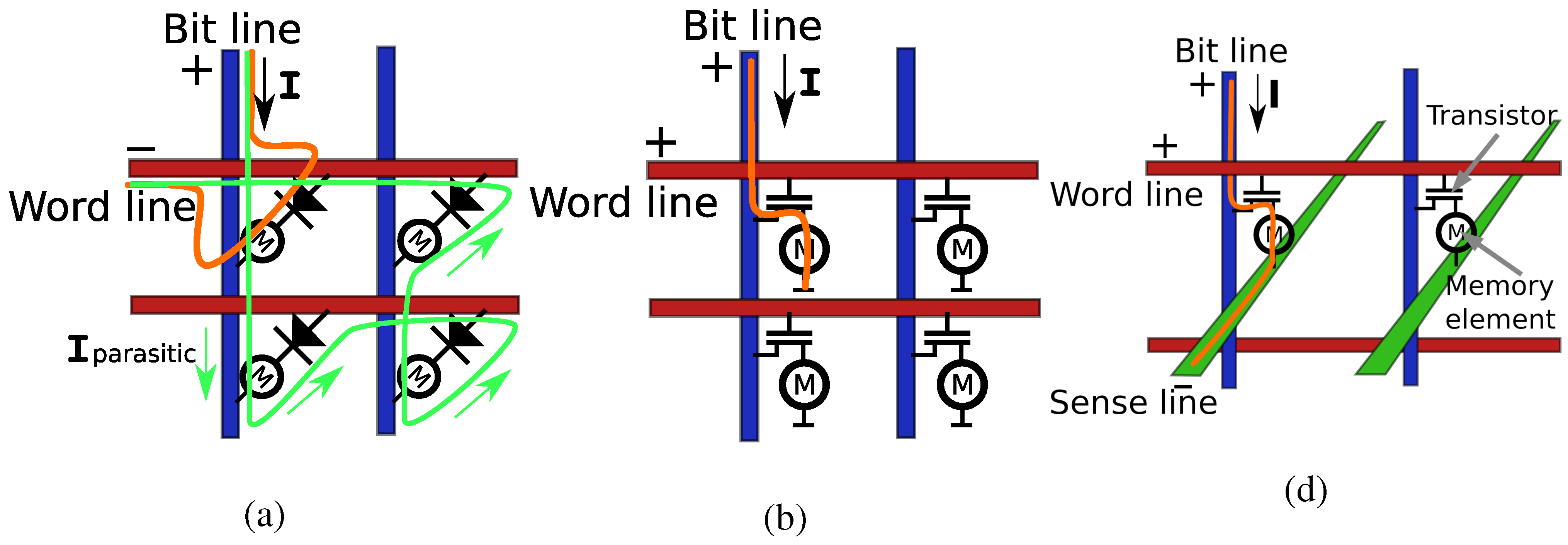
For large numbers of bit cells addressed in the cross-point architecture, we need to consider cross-talk. In two-dimensional cross-point solid state memories, every bit is addressed by connecting a voltage source to its word- and bit line (
Figure 2a). The current passing through the connection can be used to write or detect information. Since all memory elements conduct current, parasitic paths exist which shunt current around the memory element under interrogation (green lines in
Figure 2a) . These parasitic currents reduce signal-to-noise ratio and strongly limit the array size. This can be avoided by integrating a diode within the memory cell. Since shunting currents pass in the opposite direction, parasitic currents are strongly suppressed. Even though the reverse currents through the diodes are very small, the combined effect through the many shunting paths can still be too large. In a
array for instance, there are only 6 parasitic paths, but this number increases rapidly with increasing array size. In general, the number of parasitic paths for a
array is
, which can be calculated by iteration from
For large arrays the iteration can be approximated by 0.1 × 2 parallel paths. For a diode forward/reverse current ratio of 10, the maximum array size is limited to about 80 × 80.
For larger arrays, we therefore need to move towards more aggressive rejection ratios, which can be achieved by using transistors rather than diodes (
Figure 2b). Since transistors are three-wire devices, an extra wire is connected, which—even though it can be shared between memory cells—complicates the architecture. Extending the cross-point architecture into three-dimensions however, there are three wires needed to address every bit, and the transistor geometry fits perfectly (
Figure 2c).
Figure 2.
(a) 2D cross-point architecture with diodes, (b) or with transistors. (c) 3D cross point architecture with transistors. M indicates the memory storage element, which can be based on various principles.
Figure 2.
(a) 2D cross-point architecture with diodes, (b) or with transistors. (c) 3D cross point architecture with transistors. M indicates the memory storage element, which can be based on various principles.
In order to realize transistor functionality in the nanoparticles, there is some advantage in using semiconductor base materials such as silicon. Sources and drains can be defined by doping opposite faces of particles, or by assembly of n-doped and p-doped nanoparticles. Memory elements such as floating gates for charge storage (as in FlashMemory) or phase-change resistance wires exploiting the large difference in conductance between the amorphous and crystalline phase (as in PCRAM) can be incorporated at a third face or along edges of particles.
5. Magnetically Addressed
Even though particles with active electronic functionality are extremely appealing, realisation of transistors inside nanoparticles or by assembly is technologically very challenging, since it requires excellent control over doping concentrations and interface quality. As a first step towards a three-dimensional storage system however, we can store data in a passive way, keeping the detection electronics outside the self-assembled structure. Therefore one needs to avoid the parasitic current paths.
A very elegant design of a three-dimensional cross point architecture without direct connection between the addressing wires was proposed by Jay W. Forrester [
15] in 1951, based on the invention of the magnetic core memory in 1950 by An Wang and Way-Dong Woo [
16]. As Forrester writes in his introduction
In an ideal storage system it should be possible to arrange elementary storage cells in a compact three-dimensional array. Storage elements inside the volume should be selected by suitable controlling three co-ordinates along the edges of a solid array
At that time however, full 3D arrays proved to be to difficult to manufacture, and a simpler stack of 2D planes was used in implementations.
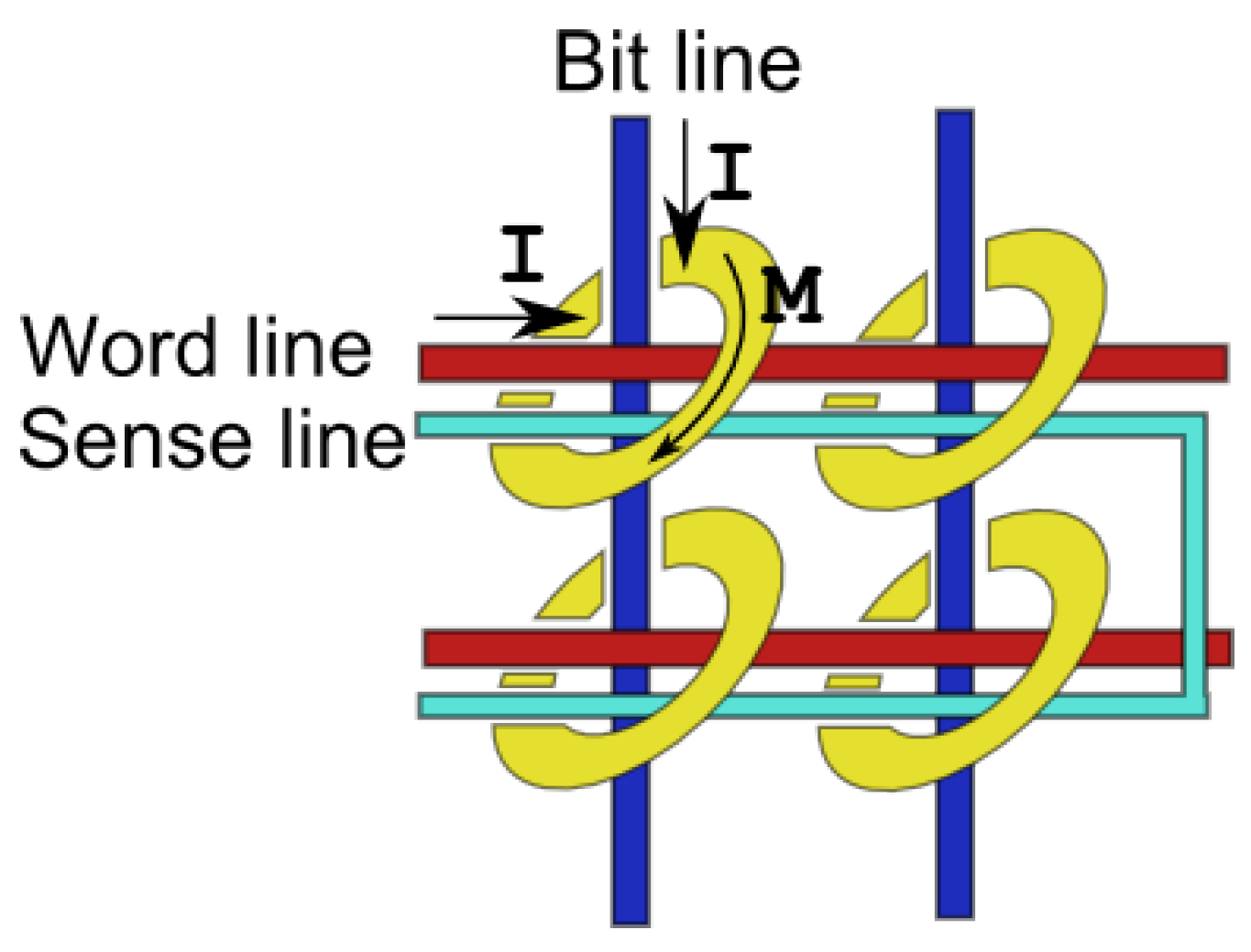
In the magnetic ring core memory, data is stored in the direction of circulation of magnetisation of tiny magnetic rings (
Figure 3 [
17]). Information is written by means of the magnetic field of wires running through the center of the rings. Individual rings can be selected by passing currents only through wires selecting that ring (coincident current writing, invented by Forrester). Only in rings where two wires are actuated, the magnetic field is sufficiently high to induce switching. The rings therefore have to be able to discriminate between currents differing by a factor of two.
Figure 3.
Magnetic core memory.
Figure 3.
Magnetic core memory.
Depending on the direction of the current, clock or counterclockwise magnetisation patterns are written, representing “1” and “0” binary information. The use of magnetic ring cores was very elegant, since in such configuration the rotation of magnetisation is zero, and no magnetic stray fields emerge, therefore limiting the cross-talk between elements.
In the 2D array, information was retrieved by attempting to overwrite information in the rings again and monitoring the change in flux. For this a current was applied to the two lines selecting a ring core (bit and word lines,
Figure 4). A third wire (sense line) passing through all cores was used to detect a change in magnetic flux, causing a induced voltage. From the presence or absence of this pulse the magnetisation direction could be derived. When a pulse was detected, an opposite current was applied to restore the state of the magnetic element (write-after-read scheme, invented by Wang).
Writing of sub-micron ring cores can be achieved in a similar way as in macroscopic ring cores. Since the magnetic volume is orders of magnitude smaller however, we need to consider the stability of the magnetisation direction at room temperature. This stability is determined by the energy barrier for magnetisation reversal, which should be higher than 40 kT for 10 year data retention. In
Appendix A. we show that for ring diameters of 135 nm with wire diameters of 50 nm, the magnetic field is strong enough to overcome energy barriers of 120 kT.
Figure 4.
Bit, word and sense lines are used to write and read information.
Figure 4.
Bit, word and sense lines are used to write and read information.
Writing as in the macroscopic system therefore seems to be possible. The situation is different for readout however. When the magnetisation reverses, the flux through the circuit formed by the sense line changes, causing an
emf. The flux change is proportional to the ring core wire diameter squared, so decreases rapidly with shrinking dimensions. The noise on the sense lines is proportional the square root of the wire resistance, so the signal to noise ratio decreases with a power 2.5. In
Appendix B. we show that this prohibits this type of destructive readout for nanometer scaled ring cores.
Figure 5.
High frequency modulation of the magnetisation can be used for non-destructive readout. (a) Magnetisation curve, (b) Susceptibility.
Figure 5.
High frequency modulation of the magnetisation can be used for non-destructive readout. (a) Magnetisation curve, (b) Susceptibility.
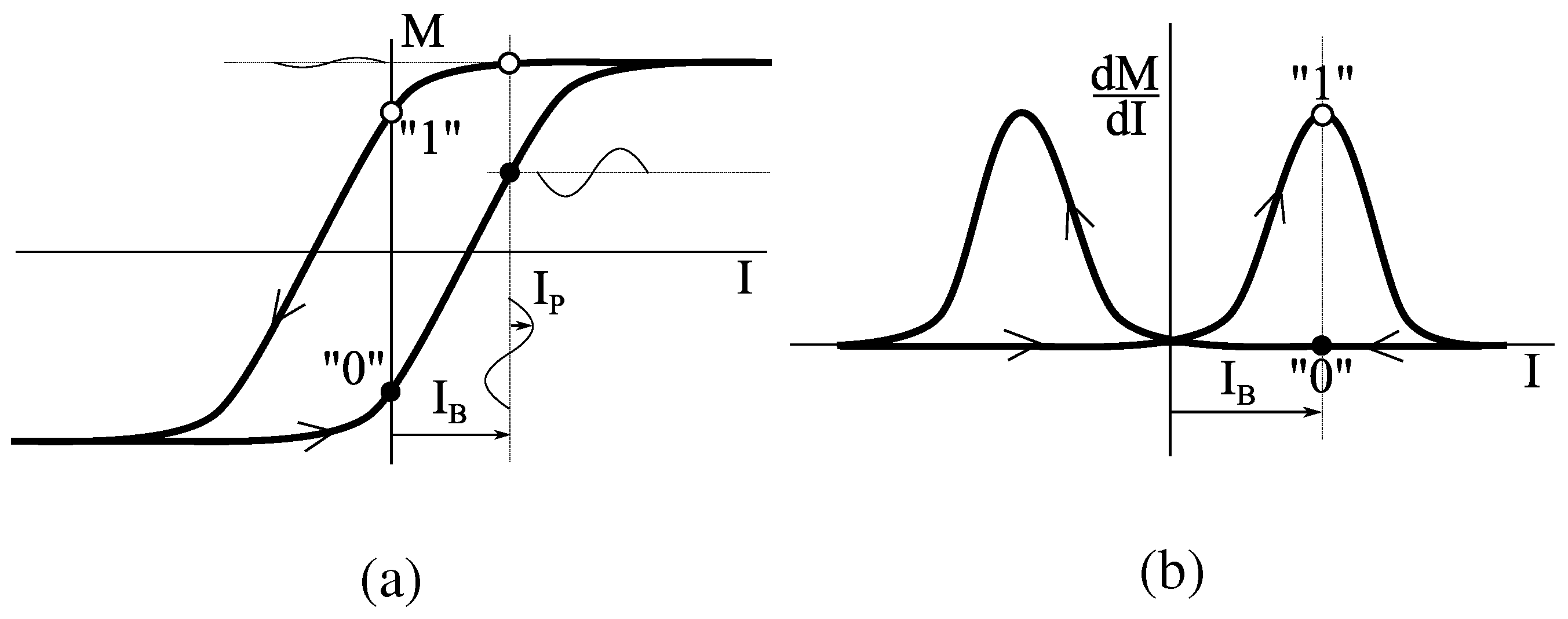
The main problem with destructive readout is that we get only one attempt to read out the information. Billing circumvents this problem by implementing a high frequency susceptibility measurement [
18]. Rather than completely reversing the magnetisation in the core, a DC bias current
below the reversal threshold is passed through one of the addressing lines and small high frequency perturbation current
through another (
Figure 5a). Since the susceptibility (
) of the core depends on the direction of the current, the
emf on the sense line can be used to determine the magnetic state of the ring (
Figure 5b). In
Appendix C. we calculate that this method will allow for sufficient signal to noise ratio, but a trade-off needs to be made between wire diameter, modulation frequency and data rate.
6. Self-Assembly of Artificial Elements
The relatively large dimension of 135 nm for bits required for a volumetric density of 4 × 10 bit/m suggests the use of nanotechnology. Volume production of features at those dimensions is commonplace. We expect that fabrication will become increasingly cheaper, and could be produced by depreciated equipment by the year 2020. Already today, methods exist to assemble these particles afterwards in large three-dimensional structures, similar to the way nature uses atoms and molecules to assemble larger structures.
The general concept is to fabricate large amounts of identical particles (spheres, cubes, tetrahedra,
etc.) which are treated in such a way that they spontaneously self-assemble in liquid or gaseous environments. One method is to produce particles which have hydrophobic and hydrophilic surfaces. When immersed in water, the hydrophobic surfaces bind together, producing irregular or crystalline agglomerates. Glotzer [
19] gives an excellent overview of the state of the art in this field, listing many different types of particles and realized assemblies.
Defect-free assembly of large arrays is challenging, and is discussed in more detail elsewhere [
20]. Generally speaking however, if the particles are relatively large they can become kinetically locked in a local minimum. One promising way to avoid this is to use templated growth, or
collodial epitaxy, for instance by using gravitational [
21], electrostatic [
22] forces or hydrophobic/hydrophilic interactions [
23].
Up to now, the particles are passive, which is useful if one wants to realize fluidic filters [
24] or photonic crystals [
25]. Although not yet demonstrated, several feasible paths to nanoparticles with internal degrees of freedom, or with electronic functions, with designed sterical and chemical anisotropy, are being considered—it is only a matter of time until they become available. Nanoparticles with a form commensurate with the crystal structure of silicon can be made by exploiting the great dependency of the etch rate in some high pH solutions. The machining of monocrystalline silicon tetrahedra is described elsewhere [
26];
Adding an electronic circuit on the particles is not a major step. The technology allows for modification of the vertices, edges and faces of the tetrahedrons by means of corner lithography [
27,
28].
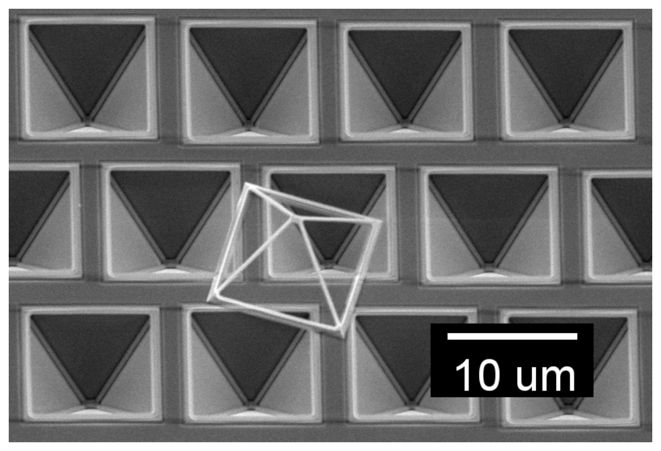
Figure 6 shows an initial result of a free SiN wireframe produced by this method. The size of the particle is determined by the etched inverse structure in the Si, which can be seen below the particle. The overall dimensions are determined by lithography, and can be reduced below 100 nm. Since the particles are still connected to the Si substrate before release, it is possible to deposit different materials in vertices, edges and faces. One possible way to achieve this is by shadow evaporation under an angle before removal of the Si, so that the Si substrate shadows the edges and faces on the opposite to the edges and faces on which deposition occurs. This can be combined with protection of faces, edges or vertices by depositing lift off materials first, again under an angle. By multiple deposition steps in specific order and at specific angles, rather complex combinations of materials can be applied, such as for instance conductors and magnetic materials, without having to resort to sub-100 nm lithography.
It has already been shown that nanoparticles can be modified to steer self-assembly into crystals so that regular structures similar to the cross-point structures shown in
Figure 1 can be grown. Parts of the nano-particles can for instance be made hydrophobic so that the assembly of amphiphilic particles into crystal structures similar to self-assembled structure in nature will become possible, see for instance [
29,
30,
31]. Alternatively, parts of the particle can be covered with organic agents or biological that get charged in a solution; by tuning the polarity quasi ionic crystals can be grown (see for instance [
32]). Even base-pair matching in DNA strands is demonstrated as a method for self-assembly [
33]. After assembly, connections can be fixed by using for instance polymerized adhesives [
34]. For an active assembly, some of the connections between particles need to be conductive, which can for instance be achieved by diffusion of gold contacts [
35]. For larger scale particles (300
μm), integration of electronics inside substrates has already been successfully demonstrated [
36].
Figure 6.
Wireframe produced by corner lithography.
Figure 6.
Wireframe produced by corner lithography.
Self-assembly of anisotropic nano-particles is currently in its infancy, however the emerging analogy with the growth of molecular crystals is quite encouraging. Regardless of the technique being used, it should in principle be possible to realize smarticles with transistor functionality or magnetic ring cores.
7. Self-Assembled Ring Core Memory
In the last part of this paper we will explore whether it would in principle be possible to realise a 3D magnetic ring core memory by means of self assembly of a limited number of substructures produced by corner lithography. Two functions need to be assembled, a three dimensional array of wires (the word, bit and sense lines) and magnetic ring cores. There are many different ways in which a three dimensional array of wires can be self assembled, starting from tetrahedra, cubes or pyramids for instance.
Table 2.
Units cells for 3D cross point architectures, using tetrahedra, cubes or pyramids as building blocks.
Table 2.
Units cells for 3D cross point architectures, using tetrahedra, cubes or pyramids as building blocks.
| | Vertices | Edges | Unit cells | Unique elements |
| Tetrahedron | 4 | 6 | 8 | 4 |
| Cube | 8 | 12 | 8 | 2 |
| Pyramid | 5 | 8 | 8 | 4 |
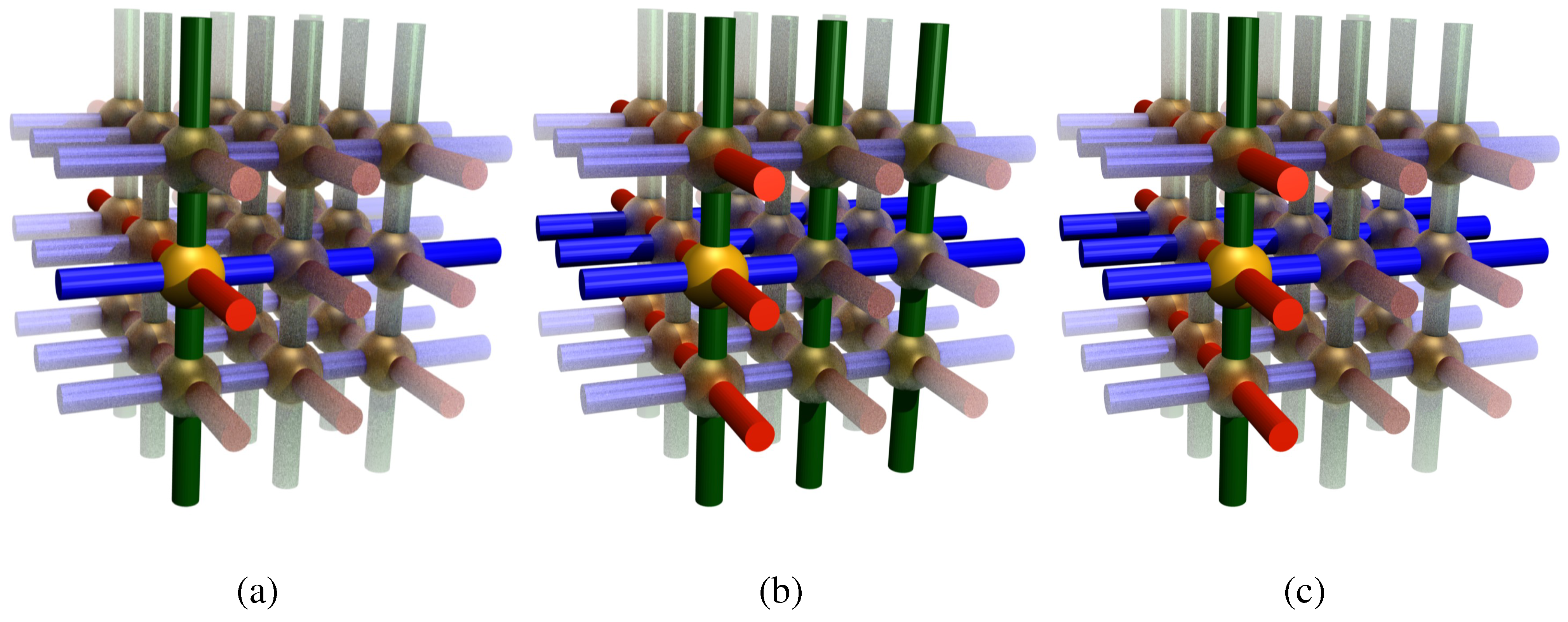
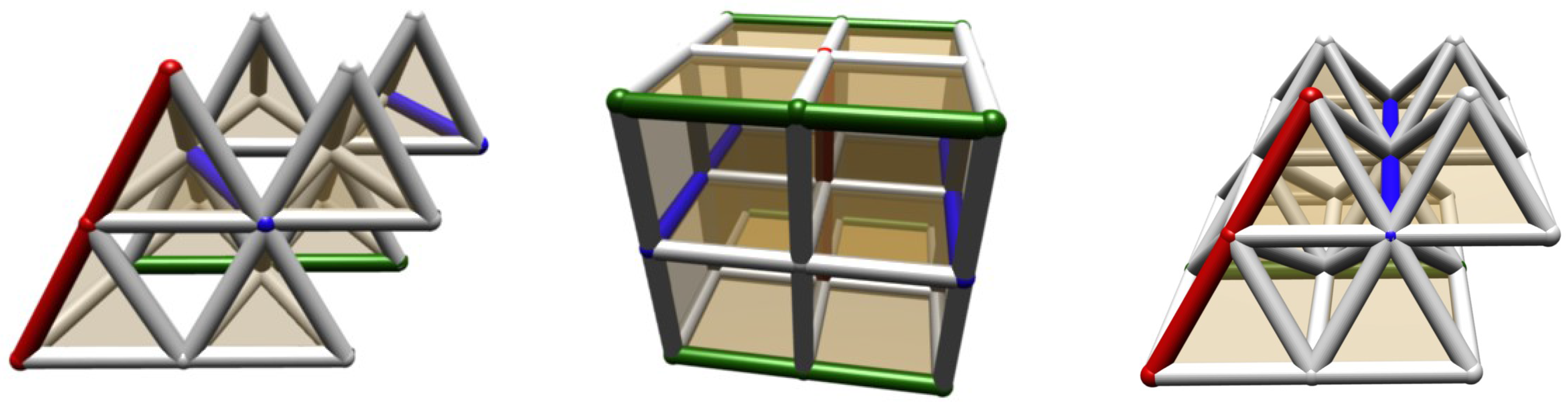
Table 2 lists the properties of unit cells constructed from these three basic elements. To realise 3D cross point architectures, for each of those basic elements eight elements are needed to realise a unit cell (
Figure 7). Tetrahedra are the simplest elements, with exactly the right number of corner points. Starting from cubes, only two types of elements are needed (with and without wires). For tetrahedra and pyramids, four different elements are combined into the unit cell.
Figure 7.
Self-assembly of wire frames (tetrahedra, cubes and pyramids) into units cells which can assemble into a 3D cross-point addressing architecture. Each unit cell contains eight smarticles.
Figure 7.
Self-assembly of wire frames (tetrahedra, cubes and pyramids) into units cells which can assemble into a 3D cross-point addressing architecture. Each unit cell contains eight smarticles.
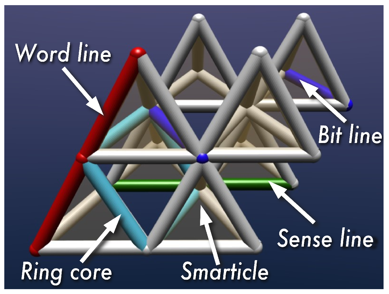
Figure 8.
By assembly of smarticles with different materials in the edges, a unit cell for a ring-core bit can be realized.
Figure 8.
By assembly of smarticles with different materials in the edges, a unit cell for a ring-core bit can be realized.
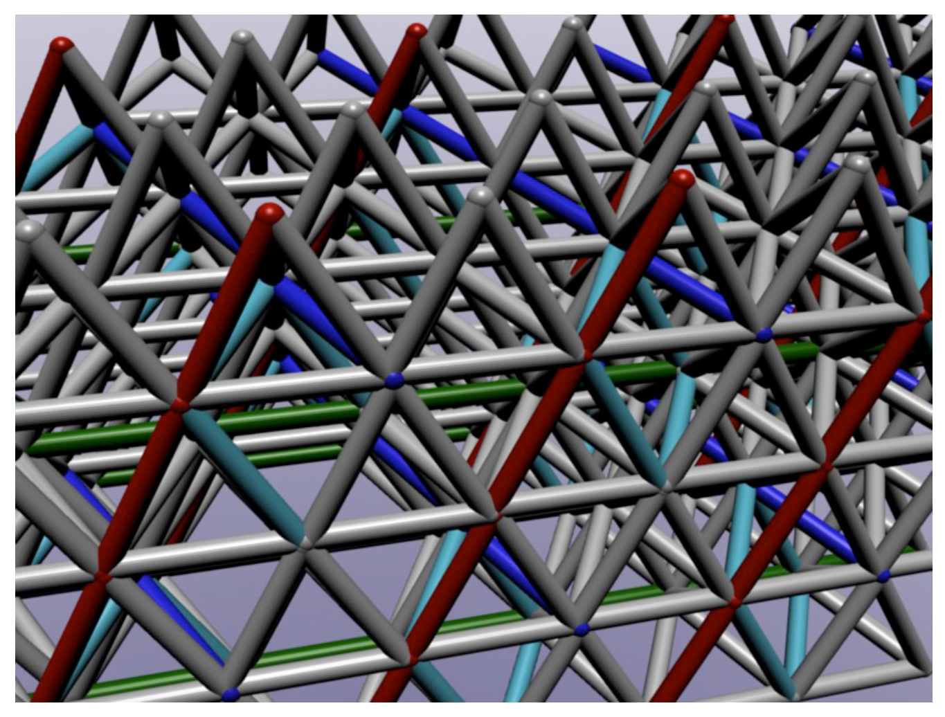
Figure 9.
Repetitive assembly of unit cells lead to a 3D ring core memory structure.
Figure 9.
Repetitive assembly of unit cells lead to a 3D ring core memory structure.
Also the magnetic ring core has to be defined by vertices. An efficient method is using tetrahedra.
Figure 8 shows a unit cell of eight tetrahedra, with addressing lines at the corners of a square magnetic ring. Of course, the addressing lines have to be located within the magnetic ring for inductive read-out, and should be electrically isolated from it. Placing the wires close to the magnetic ring has the advantage of an increase in field strength. The magnetic elements do not have to touch, since stray field coupling will lead to flux closure structures.
This particular solution requires 5 different types of elements. There are other solutions, with more favorable positioning of the magnetic core, but at this point it is sufficient to realise that in principle it is possible to construct a 3D magnetic ring core memory from a limited number of simple building blocks.
Figure 9 shows an impression of such an architecture, where the extension of the addressing lines can be clearly seen.
The technological challenges to realise a structure like this are formidable: We can make silicon terahedrons in a size range from a few tens of nanometers to a few micrometers, and we know ways to add electrical conductors of various metals along the edges. But these complex structures needs several types of tetrahedra. They have to be assembled in the right way and with perfect alignment to each other as well as the 2D-circuitry surrounding the array which is not trivial at all. Furthermore they should conduct electrical current along lines passing a vast number of particles, whilst keeping the impedance low.
8. Conclusions
We expect the increase in data density for non-volatile, two-dimensional data storage to come to a halt when the bit spacing reaches atomic dimensions, which will be at a data density of about 4 × 10 bit/m. To continue the capacity of storage systems, we need to move from surface to volumetric storage. Using typical values for package sizes, one can estimate that the onset of three-dimensional data storage will have to start at a volumetric density of 4 × 10 bit/m, or bit cell volumes of (135 nm).
By adopting the cross-point architecture from today’s solid state memories, and extending it into three dimensions, a simple addressing scheme can be made. For large arrays, selection by three orthogonal planes is favourable since it reduces the number of connections to the outside.
If the memory cells are electrically addressed, transistors are required to reduce parasitic currents. Since transistors are three-terminal devices, they fit very nicely with the three-dimensional cross point architecture. As memory elements, phase change wires could be integrated.
Parasitic currents can be avoided by re-using the magnetic addressing strategies used in ring core memories from the early years of computer technology. We calculated that storing data into magnetic ring cores at sub micron dimensions is possible, using coincident current writing at current densities well below the electromigration threshold, and energy barriers largely sufficient for 10 years of data retention. The small size of the rings prevent destructive readout at sufficient signal-to-noise ratio, but a susceptibility technique, combined with frequency mixing can certainly be applied.
A promising strategy for for the realisation of three-dimensional memories could be the self-assembly of artificial sub-micron elements (smarticles). Such elements can be realised by combining edge-lithography techniques and anisotropic etching. The first experiments into this direction are encouraging.
We show that a ring core memory can in principle be (self-) assembled from eight tetragonal wire frame elements per memory cell, consisting of five different types of tetrahedra each having different combinations of conducting, non-conducting and magnetic edges. Other configurations are nevertheless possible.
We therefore believe that the concept of a self-assembled three-dimensional ring core memory is technically feasible, and will provide an intriguing first step towards a solution for data storage beyond the atomic limit.


